Abstract
This paper presents a detailed and accurate small-signal analysis model for a four-terminal low-voltage direct current (LVDC) distribution network with distributed secondary control strategy. To tackle the contradiction between power sharing accuracy and average voltage recovery ability of voltage source converters (VSCs), a distributed secondary control strategy is adopted, which is based on average consensus algorithm and local voting protocol. Furthermore, to analyze the stability of LVDC distribution network based on the proposed distributed secondary control strategy, a detailed and accurate small-signal analysis model is formulated which is derived from various non-linear state-space sub-models. The time-domain simulation and electromagnetic simulation are carried out to verify the validity and accuracy of the proposed model. Based on this model, the influence rules of main eigenvalues are summarized with the variation of PI control and DC line parameters. Time-domain simulations conducted in PSCAD are used to validate the operational limits of the secondary controllers and DC line obtained from the small-signal stability analysis.
1. Introduction
Recently, the DC distribution system has witnessed a vigorous development because the extensive application of power electronics and large-scale access of renewable energy sources [1]. The DC distribution system has larger power supply capacity and lower line losses with simpler control schemes over traditional AC distribution network [1,2,3]. Multi-terminal DC distribution network is mainly composed by DC converter stations, distributed generations (DGs), load and energy storage systems (ESSs). It has become a research hotspot for superiorities of easy DG access and high system efficiency. The coordinated control among DC converter stations is one of the key technologies to ensure stability, reliability and optimization of the system.
The control targets of the DC converter stations usually involve voltage regulation and power optimization. Generally, the DC converter stations adopt the droop method to implement power distribution according to their own capacity without communication, which can improve the operation reliability of the system [4,5,6]. However, even though the droop control can be implemented easily, it has a contradiction between voltage regulation and power distribution due to the existence of line impedance in the DC system [7]. Therefore, a secondary control for the droop-based DC system is necessary. At present, the centralized and decentralized methods are two main ways to implement secondary control. A single central controller is designed to collect information and send reference to each unit in centralized way [8,9,10,11]. However, the reliability of centralized method is poor due to the failure of the center node or link, and the capability in plug and play is weakened by centralized communication. The decentralized method is more practical than the centralized control, because its reliability and flexibility [12]. In [13], a decentralized droop control method based on virtual resistance in DC system is proposed to compensate power distribution deviations caused by line resistances. However, this method cannot eliminate the voltage deviation. To restore the bus voltage, a hierarchical coordination control based on local information is proposed for DC distribution system to realize smooth operation in steady state and secondary voltage recovery in harsh operating condition as well as global power optimization [14]. Although the simplicity and decentralized nature of the droop control are retained by decentralized method, the global power optimization cannot be realized by only the local information.
Compared with the above two methods, the distributed secondary control method that requires only local computation and information exchange among some neighboring units through a sparse communication network has drawn more attentions [15,16,17]. Reference [7] proposes a hierarchical distributed control strategy for the DC distribution network based on the distributed average algorithm. By designing different weights of the voltage control and power control, the effective balance between the two control objectives can be achieved. A distributed control paradigm based on the reverse droop controller is established to achieve voltage regulation and proportionate load current sharing in a DC network [18]. In [19], a distributed voltage control method for distribution network is proposed to compensate the reactive power and provide the stable voltage for distribution network by using the terminal load and its corresponding power factor correction device. Reference [20] designs a two-level distributed control strategy for the wind farms by regarding the active power utilization rate as the consistent variable. To sum up, although the centralized method can achieve more complex control objectives, it has the risk of system failure. The decentralized method has higher reliability and expansibility, the control effect is not satisfactory. The distributed method can be implemented by multiple distributed controllers working in parallel, which increases the reliability, flexibility, and scalability of the control system. Table 1 lists the advantages and disadvantages according to above three methods.

Table 1.
Summaries on secondary control methods.
Therefore, the distributed manners are considered as promising options for the optimal control of the DC distribution network. In this case, a distributed secondary control strategy for enhancing the power distribution accuracy and recovering the average voltage of the DC converter stations is adopted in this paper. However, there are also many problems remained to be solved before the distributed schemes become more practical for DC distribution network. The stability of the system should be considered first, which is the foundation of voltage regulation and power distribution.
The most commonly used way for stability study is the small-signal analysis method [21]. The small-signal stability analysis of conventional power systems has been well established. More and more researches have focused on the stability analysis of low voltage DC microgrids [22,23,24,25,26] and HVDC transmission & distribution networks [21,27,28,29,30,31,32,33]. The small-signal model of the converter-based microgrid is established to investigate how circuit and control parameters give rise to the oscillatory modes and the damping performance of these modes [22]. Reference [23] establishes a small-signal model of DC microgrid and analyzes the influence laws of generation parameters to ensure the system stability. A reduced-order model of multi-terminal DC microgrid is established in [24], and the small signal stability of the system is closely related to the sag constant of the distributed generation. In [25], a general methodology considering four kinds of terminals for small-signal stability analysis is presented, which is useful for academic purposes and practical applications. An improved secondary control strategy is proposed for DC microgrid in [26], and the control parameters are optimized using small signal modeling. Similarly, the small signal model of the HV MTDC network is built in [27], and the stability of the system is analyzed. However, the stability influencing factors and countermeasures are not mentioned. Reference [28] presents a detailed state-space model of a more elaborated four-terminal VSC-MTDC system connecting two offshore wind farms to an AC network. Small-signal stability analysis is carried out to define the ranges for the gains of the VSC controllers that ensure dynamic stability. Reference [29] reviews various small-signal stability analysis tools, and the impedance stability analysis of the VSC-based HVDC transmission system is presented. Furthermore, the stability assessment of multi-terminal DC distribution system is performed through small-signal pole-zero analysis to investigate the key factors affecting the system stability in [30,31]. Additionally, a comprehensive small-signal model and stability analysis of VSC-based medium-voltage DC distribution system are performed to confirm that the proposed comprehensive model is more accurate than the simplified model and identify the guidance for the selection of PI parameters [32,33].
As discussed above, the most stability studies are based on the traditional primary control scheme or its improved one. The detailed small-signal model of multi-terminal DC distribution network should be established, and the stability analysis considering distributed secondary control needs further verification. The main contributions of this paper include:
- The detailed and accurate small-signal model of the whole multi-terminal LVDC system containing distributed secondary control is built.
- The stability of the entire LVDC distribution network is analyzed, and the effects of parameters variations on the small-signal stability are investigated by sensitivity analysis.
- The time-domain simulation by Simulink and the electromagnetic simulation by PSCAD are both conducted for the entire LVDC system to verify the accuracy of the model.
The rest of this paper is organized as follows: Section 2 introduces the structure and operation principle of the DC distribution network, including primary control and distributed secondary control. Section 3 proposes the non-linear state-space model of the DC distribution network containing secondary control. A small-signal model of the entire DC distribution network is established and verified for stability analysis in Section 4. Small-signal stability analysis is conducted in Section 5. At last, Section 6 and Section 7 present discussion and concluding remarks respectively.
2. Operation Principle of the LVDC Distribution Network
2.1. The Structure of LVDC Distribution Network
The common topology of LVDC distribution network usually includes chain structure, two-terminal structure, and ring structure. A typical multi-terminal low voltage LVDC distribution network topology is shown in Figure 1. The DC distribution system connects with the AC systems through converter stations, and it integrates the renewable resources, energy storage system, AC loads (ALs), DC loads (DLs), and so on. The renewable resources usually contain photovoltaic (PV) system and wind turbine (WT) system, which work in maximum power point tracking (MPPT) mode. The energy storage systems can absorb or inject active power from or to the network to optimize the load flow and keep the bus voltage stable when the converter stations broke down. The load can be classified into common load and important load, where the common load can be cut off to ensure the system stable in critical situation. As the converter station is dominant for the LVDC network, the coordinated control of converter stations is important for the stable and optimal operation of the whole system.
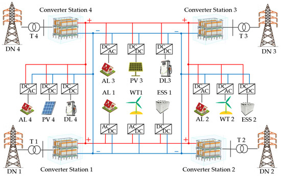
Figure 1.
Structure diagram of multi-terminal LVDC distribution network.
2.2. The Primary Control of VSC-Based Converter Station
In a multi-terminal LVDC distribution system, the coordinated control strategy of VSC-based converter station consists of primary control and secondary control. The primary control usually adopts droop method to distribute active power among all converter stations according to their capacity. The structure of a converter station and its primary control is shown in Figure 2. The primary control consists of P-V droop loop and inner loops, and the SPWM signals achieved by these control loops are applied to converter to accomplish the primary control target.
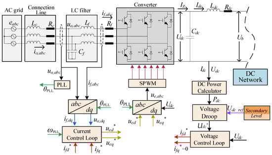
Figure 2.
Converter station and its primary control block diagram.
The P-V droop equation and voltage control loop can be expressed
where is the reference output voltage of converter station, Udc_ref is the rated voltage provided by secondary control level. The measurement unit of and Udc_ref is V. k is the droop coefficient. Pdc is the actual output power and the unit is kW. is the d-axis current reference value of inductance Lf, Udc is the actual output DC voltage and the unit is the same as . kP,U and kI,U are the parameters of the proportional-integral (PI) controller of the inner voltage loop.
The droop coefficient k can be designed as follows
where UdcN is the rated voltage of DC network, Udcmin is the minimum voltage, which can be set to 95% of UdcN. The unit of UdcN and Udcmin is V. PNmax is the maximum output power of converter station and the unit of it is kW. It can be seen from Equations (1) and (2) that the power sharing of different converter stations is in proportion to their maximum output power [34,35]. However, the DC output voltages of different converter stations are different, which causes the output power deviation between each station and decreases the utilization rate of whole stations. On the other hand, it can be concluded that the elimination of output power deviation will enhance the voltage drop level of different stations. This will increase the probability of voltage violation and the power loss in DC distribution network. Therefore, the primary control has a contradiction between voltage regulation and power distribution. In order to improve the power distribution accuracy and recover DC output voltage, a distributed secondary control strategy is implemented based on the primary control.
2.3. The Distributed Secondary Control for DC Distribution Network
As discussed above, the distributed control method requires only local computation and information exchange among some neighboring units through a sparse communication network. It can increase the reliability, flexibility, and scalability of the secondary control level. According to the secondary control target, the distributed secondary control structure of converter station is shown in Figure 3. It can be observed that the secondary control includes voltage secondary control and power secondary control. In voltage regulation step, the average DC output voltage of all converter stations is estimated, and the estimated average voltage Uave is compared with rated voltage UdcN to obtain the compensation item ΔV. In the power regulation step, the average per unit output power Paveλ is estimated, and it is compared with the local value Pdcλ of each converter station to generate the compensation item ΔU. Finally, ΔV and ΔU are added to generate the rated voltage Udc_ref for the primary level. Then, the primary control in this paper can be rewritten as follows
where ΔVi and ΔUi are the voltage compensation items.
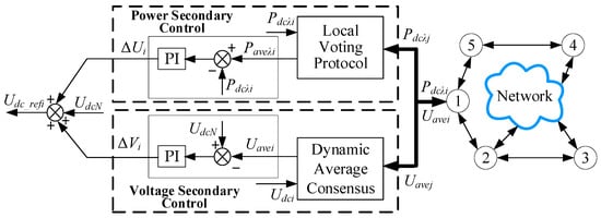
Figure 3.
Distributed secondary control structure of converter station.
As shown in Figure 3, the estimation of average voltage and per unit power are all realized by distributed algorithm. As the communication delay is too small that the sampling control cycle of the secondary level can be designed shorter. Thus, the continuous model is considered in this paper. The dynamic consensus algorithm is often used to estimate the average value of the whole measurements [36]. Let xi represents the measurement of node i, while xavei is the estimation value of global averaging. Then, the dynamic consensus algorithm can be described as follows
where aij is the element of adjacency matrix A. A = [aij] is a (0,1)-matrix with zeros on its diagonal, and the off-diagonal entry aij is one if node j∈Ni. Ni represents the set of adjacent nodes of node i, namely, a node j belongs to Ni if there exists a communication link between it and node i. It can be said that the nodes have reached a consensus if and only if xavei = xavej, for all i, j. If the communication is bidirectional, then all nodes will converge to the average value of all measurements. For converter station i, the measurements can be the DC output voltage, per unit output power, et al. Based on the dynamic consensus algorithm, the voltage regulation process can be described as follows
where CE is the control gain, kP,V and kI,V are the PI parameters of voltage secondary control. Uavei is the average voltage estimated by station i. On the other hand, in order to eliminate the deviation of per unit output power, the local voting protocol is used to estimate the average per unit value, thus the power regulation process can be described as follows
where Pdcλi is the per unit power of station i, and can be calculated by
where PNi is the rated capacity of station i. Paveλi is the average per unit output power estimated by station i. dij is the voting weight, where dij > 0 if node j belongs to Ni and dij = 0, otherwise. As the below steady state analysis shows, when the coefficient matrix D = [dij] is designed as a double-stochastic matrix, the power deviation between different stations will be eliminated asymptotically. kP,P and kI,P are the PI parameters of power secondary control.
The output voltage reference then can be calculated according to (3), and the current control loop is used to follow the current reference from the voltage control loop. The bandwidth of this loop is designed to be large enough to maintain the power balance of the converter station while load changes. Within the distributed secondary control, the average DC output voltage can be recovered and the per unit output power deviation of all stations can be eliminated, respectively.
2.4. Steady-State Analysis
Laplace Transform Method is often used to verify the steady control effect of the proposed control strategy. The Laplace Transform of Equations (3), (5) and (6) are shown as follows
where UdcN(s) = (UdcN/s)1, 1 is a n × 1 vector whose elements are all equal to one, PN = diag{PNi}, Pdcλ(s) is the Laplace Transform of [Pdcλ1, Pdcλ2, …, Pdcλn]T, Udc(s) is the Laplace Transform of [Udc1, Udc2, …, Udcn]T.
Let Ln2 = D − In, In is the unit matrix, then Ln1 and Ln2 are all the so called Laplace matrix. Suppose the system is stable, then = Udc, and substitute Equation (9) into (8)
where H(s) = diag{kP,V + kI,V/s}, G(s) = diag{kP,P + kI,P/s}. Multiplying both sides of Equation (10) by s2 and implementing the Final Value Theorem, (10) can be described as follows
where is the steady DC voltage vector, and is the steady per unit power vector. Since Equation (11) is guaranteed for any kI,V and kI,P, it can be derived that
For Equation (12), according to [37], Q = is the averaging matrix, whose elements are all equal to 1/n. Multiplying both sides by 1T, Equation (12) can be expressed as follows
For Equation (13), because Ln2 is the Laplace matrix, (13) only has one solution, that is = L*1, in other words
The above analysis shows that the per unit output power of each converter station will converge to L*, and its value is determined by the net load in the DC distribution network. That is, all converter stations will distribute their output power according to their rated capacity accurately. In addition, the average DC output voltage will converge to the rated value UdcN.
3. Non-linear State-Space Model of the DC Distribution Network
3.1. State-Space Model of the Individual Converter Station with Primary Control
To obtain the model of the entire DC distribution system, the state-space model of an individual converter station with primary control needed to be first established. In this section, all elements in the converter station system shown in Figure 2 are expressed in terms of mathematical equations as a basis for the small-signal model.
- Phase Locked Loop Equations
In earlier studies, dPLLqPLL coordinate system based on the AC input voltage uo is usually used for the small-signal modelling. However, when the transient process of PLL cannot be neglected, the state space equations should be established
where uoq is the input voltage of filter in the qPLL-axis. ω and ωo are the angular frequency of AC grid and rated angular frequency, respectively. The unit of ωo is rad/s. ωPLL is the output angular frequency of PLL. δPLL is the output angular of PLL, which is the phase deviation between uo and e, as shown in Figure 2. z is an auxiliary state variable representing the integral part of the PI controller in the PLL, and the parameters of PI controller are kP,PLL and kI,PLL.
- Input Filter Equations
A typical LC filter is composed of the filter inductance Lf and its equivalent resistance Rf, and the filter capacitor, which is given by Cf. Based on the dPLLqPLL coordinate system, the state equations of the LC filter can be presented as
where ifd and ifq are the filter inductor current in the dPLLqPLL-axis. ued and ueq are the input voltage of the converter in the dPLLqPLL-axis, respectively. uod is the input voltage of filter in the dPLL-axis. iod and ioq are the input current in the dPLLqPLL-axis. The units of Rf, Lf and Cf are mΩ, mH and μF, respectively.
- AC Connection Line Equations
The converter station is connected to the AC grid through a transmission line, which consists of resistance Rc and inductance Lc. As the AC grid is considered as an ideal source, the absolute stable dGqG coordinate system based on it is used to establish the state space equations of the transmission line
where ed and eq are the AC grid voltage in the dGqG-axis, and they are constant values with eq = 0. The unit of ed and eq is V. iod_G and ioq_G are the input current in the dGqG-axis, respectively. uod_G and uoq_G are the input voltage of LC filter in the dGqG-axis, respectively.
- Converter Equations
With the losses in switching elements (e.g., IGBTs and diodes) neglected, it can be assumed that the input voltage of the converter station will be equal to its reference value, as follows
where ued* and ueq* are the voltage reference of the inverter in the dPLLqPLL-axis.
- DC Connection Line Equations
The converter station is also connected to the DC bus through the transmission line, with the line parameters consisting of resistance Rdc and inductance Ldc. The state space equations of the DC connection line are given as follows
where Idc is the current of transmission line, and Udc is the DC output voltage of capacitor Cdc. Ig is the output current of converter and Ub is the voltage of DC bus. The measurement units of Cdc, Ldc and Rdc are F, mH and mΩ, respectively.
- Power Calculator
The power calculator is applied in this case for calculating the instantaneous active power. With the losses neglected in converter station, the AC active power is equal to the power transmitted to the DC port, which is shown in (21)
where ωc is the cut-off frequency of low-pass filter and the unit is rad/s.
- Voltage and Current Loop Control
The voltage and current loop control block diagram are shown in Figure 4 in detail. kP,U and kI,U are the parameters of the PI controller of the outer voltage loop, and kP,C and kI,C are the parameters of the PI controllers of the inner current loop. The DC output voltage reference () of converter station is obtained through droop equation and the secondary control value ΔV and ΔU, as mentioned in Section 2.2.
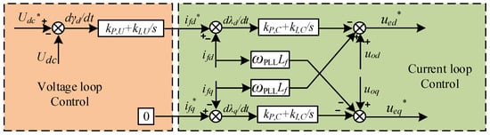
Figure 4.
Voltage and current loop control block diagram.
According to Figure 4, the space state equations of voltage and current loop control can be written
where state variables γ and λ are defined to assess the dynamic properties of the PI controllers in the voltage and current loop, and the corresponding state equation in the dPLLqPLL-axis is shown as
3.2. State-Space Model of the Distributed Secondary Control
According to the proposed distributed secondary control strategy described by (5) and (6), the space state model is described as follows
The state variable Φv = [Φv1, Φv2, …, Φvn]T is defined to describe the error accumulation between estimated voltage and rated voltage, while Φp = [Φp1, Φp2, …, Φpn]T is defined to describe the error accumulation between estimated per unit power and local per unit power. The corresponding state equation is
where UdcN = UdcN1, Uave = [Uave1, Uave2, …, Uaven]T, Ues = [Ues1, Ues2, …, Uesn]T.
3.3. State-Space Model of the DC Distribution Line and Load
As different DC network topologies have different state space models, the four-terminal ring topology DC distribution network is taken for the example in this paper to establish the state space model, as shown in Figure 1. On the other hand, the wye-delta transform is adopted to simplify the DC distribution line and load model, thus the equivalent model of the DC distribution network line and inner constant power load (CPL) is shown in Figure 5.
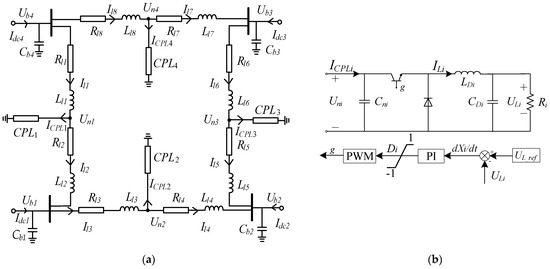
Figure 5.
The model of DC distribution network line and inner constant power load. (a) Equivalent circuit of the DC distribution network; (b) Equivalent circuit of the constant power load.
- DC Distribution Line Equations
As Figure 5a shows, all the converter stations are connected to each other through DC distribution lines. The state space equations of lines are written as follows
where Un is the node voltage of the equivalent constant power load, Il is the branch current, Ll and Rl are line inductance and resistance, respectively. Cb represents the grounded capacitance. ICPL is the current of CPL. The measurement units of Ll, Rl and Cb are mH, Ω and μF, respectively
- Constant Power Load Equations
As Figure 5b shows, the equivalent constant power load in the DC distribution system is modeled as DC/DC bulk converter. The state space equations are as follows
where Cn, LD, CD are the parameters of DC/DC bulk converter, respectively. UL and IL are the capacity voltage and inductor current of resistance side. UL_ref is the rated voltage, and R is the equivalent resistance of load. D is the duty ratio of control signal, kP,L and kI,L are the parameters of the PI controller of the converter. The measurement units of LD, CD and Cn are mH, mF and mF, respectively.
4. Small-Signal Model of the DC Distribution Network Based on Distributed Secondary Control
4.1. Small-Signal Model of the DC Distribution Lines and Loads
Based on (26) and (27), the small-signal state space model contains 28 state variables and 4 output variables, which are given by
Thus, the small-signal equation and the output equation are as follows
where ΔIdc = [ΔIdc1, ΔIdc2, ΔIdc3, ΔIdc4]T and ΔR = [ΔR1, ΔR2, ΔR3, ΔR4]T. Both of them are the input variables. Appendix A shows the coefficient matrix As0, Bs0, Cs0, Ds0.
4.2. Small-Signal Model of the Multiple Converter Stations
As previously discussed, all the state space equations needed for modeling the converter stations have been introduced. Based on (16)–(23), the state space model of i-th converter station without proposed distributed secondary control contains 14 state variables and 3 output variables (ΔIdci, ΔPdci, ΔUdci)
The small-signal equation of i-th converter station then can be described as follows
where Ui = [ΔVi, ΔUi]T, Ei = [edi, eqi]T. As there are four converter stations in the DC system, the entire small-signal model is established as follows:
where Δxs1 = [Δxvsc1T, Δxvsc2T, Δxvsc3T, Δxvsc4T]T, ΔUb = [ΔUb1, ΔUb2, ΔUb3, ΔUb4]T, Δω = [Δω1, Δω2, Δω3, Δω4]T, U = [ΔV1, ΔU1, ΔV2, ΔU2, ΔV3, ΔU3, ΔV4, ΔU4]T, ΔE = [Δed1, Δeq1, Δed2, Δeq2, Δed3, Δeq3, Δed4, Δeq4]T. As1 = diag(Avsc1, Avsc2, Avsc3, Avsc4), Bs1= diag(Bvsc1, Bvsc2, Bvsc3, Bvsc4), Cs1 = diag(Cvsc1, Cvsc2, Cvsc3, Cvsc4), Ds1 = diag(Dvsc1, Dvsc2, Dvsc3, Dvsc4), Es1 = diag(Evsc1, Evsc2, Evsc3, Evsc4).
The output equations are as follows
where ΔIdc = [ΔIdc1, ΔIdc2, ΔIdc3, ΔIdc4]T, ΔPdc = [ΔPdc1, ΔPdc2, ΔPdc3, ΔPdc4]T, ΔUdc = [ΔUdc1, ΔUdc2, ΔUdc3, ΔUdc4]T. Appendix B shows the coefficient matrix Avsci, Bvsci, Cvsci, Dvsci, Evsci, Fs1, Gs1, Hs1.
4.3. Small-Signal Model of the Proposed Distributed Secondary Control
According to (24) and (25), there are 12 state variables and 4 output variables in the state space model, which are Δxs2 = [Δϕv1, Δϕv2, Δϕv3, Δϕv4, Δϕp1, Δϕp2, Δϕp3, Δϕp4, ΔUave1, ΔUave2, ΔUave3, ΔUave4]T and ΔPdc = [ΔPdc1, ΔPdc2, ΔPdc3, ΔPdc4]T. The small-signal equation and output equation are described as follows
Finally, the small-signal model of the entire DC distribution network can be obtained as follows
where Δxs = [Δxs0T, Δxs1T, Δxs2T]T and represents all state variables in the DC distribution network. ΔR represents the small variation of constant power load. Δω represents the small frequency variation of AC grid, and ΔE represents the small voltage magnitude variation of AC grid. Appendix C shows the coefficient matrix As2, Bs2, Cs2, Ds2, Es2, Fs2, As, Bs, Cs, Ds.
4.4. Verification of the Established Small-Signal Model
In this section, the results from the time-domain simulation in MATLAB/Simulink and electromagnetic simulation in PSCAD are presented for the verification of the proposed small-signal model. The structure of the LVDC distribution network for case study is shown as Figure 1. There are four converter stations, and the DC sources (PV, WT, DC loads) are integrated as a constant power load for simplicity. Thus, there are four CPLs in the network. The parameters of the DC distribution network and four converter stations are shown in Table 2. The communication topology of the stations is a ring, and its corresponding adjacency matrix A and coefficient matrix D are shown in Figure 6.
Table 2.
The parameters of DC distribution system.
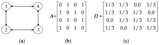
Figure 6.
The communication topology and its corresponding matrix. (a) The ring topology of the communication line; (b) The adjacency matrix; (c) The coefficient matrix.
Initially, all the DC loads (about 323 kW) are connected to the network, and all converter stations are accessed to low voltage AC grid. The main steady operation points of the system obtained by Simulink are that is equal to [808 V, 798 V, 796 V, 798 V], is equal to [135.2 kW, 67.6 kW, 67.6 kW, 67.6 kW]. It is clearly that the average voltage of DC side is 800 V, and the per unit output power of all converters are all 0.75. Thus, the effectiveness of the distributed secondary control is verified. The introduced small disturbance is a 5 kW step change of the CPL1 from 80 kW to 85 kW at 3.5 s. The curves of different state variables (Un1, Pdc1, Udc1, Idc1, uoq1, uod1, ifq1, ifd1) obtained using the small-signal model and electromagnetic simulation are compared in Figure 7. It can be seen from Figure 7 that the time-domain responses of different state variables calculated by the established small-signal model using MATLAB coincide with those obtained by PSCAD simulation. This indicates that the accuracy of the established small-signal model is suitable for the stability analysis of the DC distribution network.
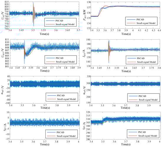
Figure 7.
Responses of different state variables to the load disturbance.
5. Small-Signal Stability Analysis
The system eigenvalues are calculated and listed in Table 3 based on the parameters in Table 2. In the small-signal analysis, it is necessary to quantify the contribution of each state to a specific eigenvalue according to [38]. Thus, the major participants of each eigenvalue are exhibited in Table 3 as well.
Table 3.
The system eigenvalues.
As shown in Table 3, all eigenvalues have negative real parts indicating a stable operating condition for the system. It can be also seen that these eigenvalues fall in to three different clusters, namely, the high damped modes, the medium damped modes and low damped modes. The participation factor indicates that the inductive current of LC filter and inner current loop influence greatly the high damped modes λ1–λ16. These modes are not detrimental to the system stability. The medium damped modes λ17–λ63 are associated with the states of DC network (DC line currents, bus voltages, node voltages) and their effects on the AC side input currents and voltages. Additionally, the low damped modes considered as the dominate modes are associated with the states of secondary control. These dominate modes are greatly influenced by the parameters of secondary control and PLL. Moreover, the DC line parameters can be also selected to optimize the transient behavior of the DC network.
By plotting the eigenvalue loci in the complex plane, the impacts of the main parameters (such as the PI parameters of the secondary control, communication delay, the parameters of PLL, and the impedance parameters of DC distribution) on system dynamics can be observed. The eigenvalue loci in the complex plane with parameters variations are shown in Figures 8, 12, 13 and 15. In Figures 8, 12, 13 and 15, the eigenvalues are marked with stars. The arrows indicate the direction of the parameter variation and black circles indicate the parameters of critical stability. For simple analysis, only the important eigenvalues are plotted. The following subsections emphasize on the influence of these parameters on the system dynamics.
5.1. Distributed Secondary Controller Effect
This section presents the impact of the secondary voltage and power controller parameters kP,V, kI,V, kP,P and kI,P on the small-signal stability and the verification of the stable region through PSCAD simulation results. When the individual parameter is considered and changed for plotting eigenvalue loci, the other parameters are all consistent with the value as presented in Table 1. The varying range of individual parameter kP,V, kI,V, kP,P and kI,P is 1 to 50, 1 to 150, 1 to 10,000 and 1 to 300,000, respectively. The eigenvalue loci are shown in Figure 8, and Figure 9 shows the time-domain simulation results through PSCAD.

Figure 8.
Eigenvalues loci (only the important eigenvalues shown) for a parametric variation of the PI parameters of secondary control:(a) kP,V in a range from 1 to 50; (b) kI,V in a range from 1 to 150; (c) kP,P in a range from 1 to 10,000; and (d) kI,P in a range from 1 to 300,000.
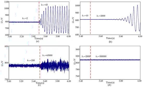
Figure 9.
Simulation results from PSCAD: (a) variation curve of Un1 when kP,V changes; (b) variation curve of Udc1 when kI,V changes; (c) variation curve of Un1 when kP,P changes; (d) variation curve of Udc1 when kI,P changes.
With a variation of proportional parameter kP,V, which changed from 1 to 50, the parametric eigenvalue analysis is repeated. In the overview of the eigenvalue loci shown in Figure 8a, λ80–82 move towards the left half of the complex plane along the real axis. The eigenpair λ64,65 also move towards left, which indicates that the real part of λ64,65 decrease while the damping ratio increase. Eigenvalue λ83 moves towards the original point along the real axis, and the eigenpair λ53,54 move towards the right part of the complex plane with the real part increasing dramatically. Furthermore, when the value of kP,V is larger than 39.8, an obvious vibration appeared, and the λ53,54 enter into the unstable region of the complex plane that bringing about the instability of the system.
Figure 8b exhibits the eigenvalue loci of the integral parameter kI,V changing from 1 to 150, where eigenpair λ53-54 are neglected due to unobvious changes in their locations and are not discussed in the following. With the increasing of kI,V, it is clear that eigenvalues λ80–83 all approach the original point along the real axis and the eigenpair λ64,65 move towards the right half of the complex plane gradually. When the value of kI,V is larger than 118.5, the λ53,54 cross the imaginary axis, which means that they enter into the unstable region of the complex plane, generating the instability of the system.
Figure 8c shows the eigenvalue loci of the parameter kP,P changing from 1 to 10000. For the power secondary control, eigenpairs λ53,54, λ66,67, λ68,69 and λ70,71 are discussed and analyzed here. It can be seen that with the kP,P increasing, λ70,71 move towards the left direction with the imaginary part becoming zero, which indicates that the oscillation of the output power disappears gradually. Meanwhile, λ66,67 and λ68,69 move towards the opposite direction with the imaginary part becoming zero and real part increasing. In addition, λ53,54 move towards the right part of the complex plane fast and as soon as kP,P is more than 7500, λ53,54 cross the imaginary axis immediately, resulting in unstable operating state.
The integral parameter of power secondary control kI,P is also the main parameter influencing the system stability. Figure 8d reveals the eigenvalue loci with kI,P varying from 1 to 300,000. Eigenpair λ53,54 is neglected while λ64,65 is added in the following analysis. In Figure 8d, λ66,67 turn to the left part of complex plane with moving towards the right direction at first. Eigenvalues λ64,65, λ68,69 and λ70,71 have the same changing patterns, that is the imaginary parts move up and down respectively and the absolute value of imaginary parts increase with the parameter adding up, which means the system would experience a slow response.
To verify the eigenvalue loci shown in Figure 8, the time-domain responses of the multi-terminal LVDC distribution network simulated in PSCAD are plotted, as presented in Figure 9. Figure 9a shows that when kP,V steps from 2 to 45 at 3.5 s, the state variable Un1 experiences an amplitude oscillation, which corroborates the results obtained in Figure 8a. Similarly, Figure 9b indicates that when kI,V steps from 10 to 2000 at 3.5 s, the DC voltage Udc1 experiences an amplitude oscillation. However, this oscillation happens at 3.7 s and the value of kI,V in this period is far larger than 118.5 shown in Figure 8b. Furthermore, Figure 9c shows the time-domain simulation results when kP,P changes from 200 to 65,000. It can obviously be seen that state variable Un1 undergoes an amplitude oscillation as well. Nevertheless, the value of kP,P is still well over the stable region shown in Figure 8c. It indicates that the accuracy of MATLAB simulation is a little higher than the results simulated in PSCAD. As shown clearly in Figure 9d, when kI,P varys from 2000 to 500,000, the curve of Udc1 stay unchanged, which is in agreement with the results obtained in Figure 8d.
According to the above analysis, the design rule of PI parameters of secondary control for the system stability can be concluded as follows:
- The augment of kP,V and kI,V may decrease the relative damping with low-frequency eigenvalues, which goes against the system stability. Too large a value of kP,V and kI,V can cause low-frequency oscillation in the multi-terminal LVDC distribution network.
- Within the range of system stability, the gradual increase of kI,P will decrease the damping ratio of the low-frequency eigenvalues. Furthermore, system also has the possibility of losing stability in the condition of large value of kP,P.
5.2. Time Delay Effect
This section presents the impact of the time delay on the small-signal stability and the verification by PSCAD simulation. The impact of time delay cannot be neglected when the sampling rate of the secondary control level is very high. In order to study the impact on system stability, the expression of delay e−τs should be simplified firstly. Using the first-order approximation of the Taylor series expansion, the e−τs can be written as follows
When the delay is small, the equation above stands. Obviously, the equation is a first-order lag function, which will bring a state variable. Based on the simplified equation, the distributed secondary control with communication delay τ can be described as follows
Finally, replace the original state-space model of the distributed secondary control with Equation (40), the small-signal model of the entire DC distribution network with time delay can be obtained as follows
where, Δ is the state variable including the new variable Δ and Δ, which are related to time delay. These eigenvalues related to time delay are calculated and listed in Table 4 based on the parameters of DC distribution network and τ = 3 ms.
Table 4.
The new eigenvalues.
As shown in Table 4, all new eigenvalues have negative real parts indicating a stable operating condition for the system when τ = 3 ms. That is, the small delay has little impact on the stability of the system. In order to study the impact of large delay, the eigenvalue loci are plotted according to different time delay. The varying range of time delay is 3 ms to 50 ms, and the eigenvalue loci are shown in Figure 10.
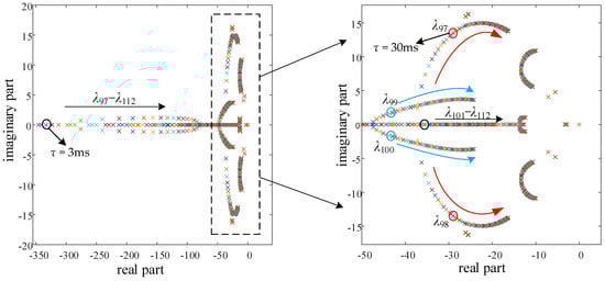
Figure 10.
Eigenvalues loci for the time delay variation of the secondary control.
With the increasing of τ, it is clear that all eigenvalues approach the original point along the real axis first. Then, all the eigenvalues are equal to −50 at τ = 20 ms. From then on, some eigenvalues’ imaginary parts begin to increase, and they move towards the right half of the complex plane gradually. From Figure 10, it can be indicated that the system is still stable during 3 ms to 50 ms, however, the stability of the DC distribution network is weakened. With the increasing of τ, the oscillation will appear on the estimated average voltages, and the damping ratio decrease gradually. Furthermore, the simulation by PSCAD is implemented as shown in Figure 11. From Figure 11, it can be seen that the will appear low-frequency oscillation after a small disturbance when τ = 30 ms, while the responses are smooth when τ = 3 ms. The damped time of the oscillation is about 0.42 s, which is similar with the result in Figure 10. Thus, the time domain simulation verifies the results from eigenvalue analysis in Figure 10.
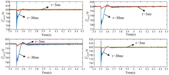
Figure 11.
Responses of state variable at the condition that τ = 3 ms and 30 ms.
5.3. Phase Locked Loop Effect
This part mainly discusses the effects of PI parameters of phase locked loop on system stability. The secondary control parameters are all original parameters presented in Table 2 when PI parameters of PLL are studied. The changing range of PI parameters are 1 to 520 and 1 to 1000 respectively. The eigenvalues loci are plotted in Figure 12.
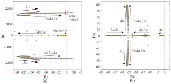
Figure 12.
Eigenvalues loci (only the important eigenvalues shown) for a parametric sweep of the PI parameters of PLL: (a) kP,PLL in a range from 1 to 520; (b) kI,PLL in a range from 1 to 10,000.
For phase locked loop, with kP,PLL and kI,PLL varying, the eigenvalue loci are shown in Figure 12. In Figure 12a, it is clearly found that λ88,91 move towards the left direction, which means they have little impacts on system stability when kP,PLL changes. Apart from these, eigenvalue λ81,82,83 as well as eigenpairs λ25,26, λ29,30, λ31,32 and λ37,38 move towards the right part of complex plane with kP,PLL varying gradually. One point to note is that, when the value of kP,PLL is up to 502.5, the stablity of system will face threats due to eigenpairs λ25,26, λ29,30, λ31,32 and λ37,38 cross the imaginary axis.
Figure 12b shows the eigenvalue loci with kI,PLL varying from 1 to 1000. Eigenvalues λ81,82,83 all move towards the left direction along the negative real axis while λ89,91 move towards the opposite direction. Furthermore, the absolute values of imaginary part of eigenpairs λ72,73, λ74,75, λ76,77 and λ76,77 increase as kI,PLL changed from 1 to 1000, which means that the damping ratio decrease slowly. Although the response speed of the system declines, the stability of it still can be ensured.
According to the above analysis, the design rule of PI parameters of phase locked loop for the system stability can be concluded as follows:
- The augment of kP,PLL has an important effect on the medium damped modes. Too large a value of kP,PLL can cause an unstable state of system.
- The parameter kI,PLL has something to do with the system oscillation. And the increase of kI,PLL may decrease the damping ratio with high-frequency eigenvalues without affecting the system stability.
5.4. DC Distribution Line Effect
According to the analysis above, the DC line parameters also have an impact on the system’s stability. Here, the effects of DC inductance Ll1–Ll8 and DC resistance Rl1–Rl8 are considered and studied shown in Figure 13, where the varying scopes of Ll1–Ll8 and Rl1–Rl8 are 3.2 × 10⁻⁵ H to 3.2 × 10⁻³ H and 0.01 Ω to 1 Ω respectively. Simulations in PSCAD with parameters varying confirm the correctness of stable region as shown in Figure 14.
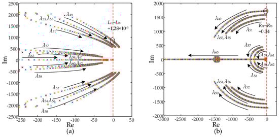
Figure 13.
Eigenvalues loci (only the important eigenvalues shown) for a parametric sweep of Ll1–Ll8 and Rl1–Rl8: (a) Ll1–Ll8 in a range from 3.2 × 10⁻⁵ H to 3.2 × 10⁻³ H; (b) Rl1–Rl8 in a range from 0.01 Ω to 1 Ω.
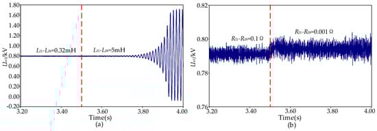
Figure 14.
Simulation results from PSCAD: (a) variation curve of Un1 when Rl1-Rl8 change; (b) variation curve of Un1 when Ll1-Ll8 change.
In Figure 13a, all eigenvalues including λ49–63 move towards the right part of complex plane as parameters Ll1-Ll8 changed from 3.2 × 10⁻⁵ H to 3.2 × 10⁻³ H. When Ll1–Ll8 are all set to 1.28 × 10⁻³ H, the eigenpairs λ49,50, λ53,54 and λ55,56 all enter into the right part of complex plane, indicating that system lose stability. It is noted that when the parameters of Ll1–Ll8 are 1.28 × 10⁻³ H, the first eigenvalues crossing the imaginary axis are λ49,50, whose major participants are Un1–Un4.
Figure 13b shows the eigenvalue loci in the parametric sweep of Rl1–Rl8 varying in the range of 0.01 Ω to 1 Ω. Eigenvalues λ49–63 all move towards the imaginary axis or along the imaginary axis in a left direction. Especially, when the value of Rl1–Rl8 is less than 0.04 Ω, the eigenpairs λ49,50 exist in the right part of the coordinate system, causing system unstable.
Figure 14a indicates that when Ll1–Ll8 steps from 0.32 mH to 5 mH at 3.5 s, the voltage of CPL1 Un1 experiences an amplitude oscillation. This oscillation is unobvious at the beginning and becomes conspicuous after 3.7 s and it is a divergent oscillation, which demonstrates that there is small-signal instability appearing in the system when inductance parameter is larger than 1.28 mH. Similarly, in Figure 14b, when Rl1–Rl8 step from 0.1 Ω to 0.001 Ω at 3.5 s, the state variable Un1 also experiences an amplitude oscillation apparently. The unstable state after 3.5 s demonstrates that the time-domain simulation results are in agreement with the stable region obtained in Figure 13b and small value of Rl1–Rl8 might cause instability. Moreover, the influence of Rl1–Rl8 is not as obvious as that of Ll1–Ll8.
According to the above analysis, the design rule of parameters Ll1–Ll8 and Rl1–Rl8 of DC line for the system stability can be concluded as follows:
- The increase of Ll1–Ll8 has significant influences on the medium damped modes and low damped modes. Too large a value of Ll1–Ll8 can cause an unstable state of system.
- The augment of Rl1–Rl8 may increase the relative damping with low-frequency and medium-frequency eigenvalues. Too small a value of Rl1–Rl8 has a tendency of causing system to lose stability.
These rules are significant for parameters design and optimization of the multi-terminal LVDC system such as PI parameters of the secondary control, which are the key parameters for VSC control. During the parameters design based on the small-signal model analysis, it must be ensured that all the eigenvalues of the system in every frequency range are provided with enough damping. The parameter design for the multi-terminal LVDC system must combine the stability of the eigenvalues in every frequency range.
5.5. Different Load Effect
This part mainly discusses the effects of constant power load (CPL) and resistance load on system stability. The CPL is the load whose electricity power does not change, while the resistance load will change according to the voltage. The eigenvalues of the system are used to explain the influence of different loads on system stability. Further, the simulation in time domain is implemented to illustrate the stability problem. Firstly, the DC distribution network with CPL and the DC distribution network with resistance load are modeled respectively based on the small signal modeling method presented in this paper. Then, the eigenvalues can be calculated based on As_CPL and As_RES, where As_CPL is the state matrix of the CPL system, and As_RES is the state matrix of the resistance system. The eigenvalues or modes that are related to Udc, Idc, Un and Il are shown in Figure 15.
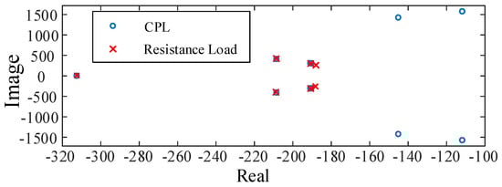
Figure 15.
Eigenvalues of CPL based DC distribution network and resistance load based DC distribution network.
From Figure 15, it can be seen that the number of eigenvalues of As_CPL is more than that of As_RES, because the CPL will bring extra modes from DC/DC converter. The both systems are stable, however, the extra modes that the CPL generated have a large imaginary part, and they are closer to real axis. Thus, it can be indicated that the variation of CPL will bring higher oscillation (about 239 Hz), and the damped time will be longer. However, the modes of resistance system have a smaller imaginary part, and the oscillation frequency is about 80 Hz. Moreover, the damped speed is faster. From the distribution of eigenvalues of different systems, the resistance load has a less impact on the stability of the system. Additionally, the simulation by PSCAD is implemented as shown in Figure 16. From Figure 16, it can be seen that the Udc, Idc, and Un will appear high-frequency oscillation after a 4 kW CPL is connecting to network. The damped time of the oscillation mode is about 0.046 s, which is similar with the result in Figure 15. In the same condition, the voltage and current change gently after the 4 kW resistance load is connecting to network. Thus, the time domain simulation verifies the results from eigenvalue analysis in Figure 15.
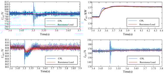
Figure 16.
Responses of different state variables to the different load disturbances.
6. Discussion
In this paper, a small-signal modeling procedure of a four-terminal LVDC distribution network with distributed secondary control is presented and analyzed. The main focus is the small-signal analysis where eigenvalue analysis and major participants analysis are adopted. The benefit of modular method is the rapidity and scalability of the small-signal modeling. In other words, the procedure of modeling is suitable for multi-terminal LVDC system. The presented procedure of modeling considers three main aspects containing individual converter stations, distributed control part and DC distribution line/load.
With the established small-signal model, the rules of system eigenvalues varying caused by the change of some parameters are carried out and analyzed. In Section 5, distributed secondary controller effect, phase locked loop effect and DC distribution line and load effect on system small-signal stability are considered. On the basis of presented results, some important influence laws are displayed in paper which indicate that PI control parameters of distributed secondary control and DC distribution line parameters such as inductance and resistance have a relative significant effect on system voltage stability through eigenvalue loci and simulations on PSCAD. Moreover, the operational limits of studied parameters are given in this study. The time-domain simulation by PSCAD is conducted for the entire LVDC system to verify the operational limits of the model, and the design rules are given for main parameters of the four-terminal LVDC distribution network, which gives a guideline for future practical parameter selection. The presented analysis only considered some important parameters, and the analysis with some other parameters varying can be studied in the future research.
7. Conclusions
A distributed secondary control method for VSCs and a detailed and accurate small-signal analysis model for a four-terminal LVDC distribution network are presented in this paper. Compared with traditional control method, the adopted secondary control strategy based on average consensus algorithm and local voting protocol can promote the power distribution accuracy while increasing the average voltage. This paper focuses on the small-signal stability analysis for the multi-terminal LVDC distribution network. Firstly, various non-linear state-space models of individual entities including individual VSC with primary control, distributed secondary control and DC distribution line/load are built. Secondly, small-signal model of the entire system is established based on individual non-linear state-space model. The accuracy of the proposed model is further assessed through a comparison between the results from the electromagnetic simulation in PSCAD and small-signal model in MATLAB. At last, eigenvalue analysis and major participants analysis are adopted to study the effects of main parameters on the stability of the system involving PI control, time delay and DC distribution line or load. However, the presented results are valid for LVDC distribution network only. If the system’s voltage is higher than the studied one in this paper, the MMC structure should be adopted for the converter station. Then, the modeling will be more complicated and the small-signal analysis need more consideration. Furthermore, the time-domain simulation results will be supplemented and verified through laboratory simulation for the next research direction.
Author Contributions
Methodology, Z.L.; Validation, M.Z.; Writing—original draft, M.Z.; Writing—review & editing, Q.W. and W.H. All authors have read and agreed to the published version of the manuscript.
Funding
This research was funded by Open Foundation of Jiangsu Key Laboratory of Smart Grid Technology and Postgraduate Research &Practice Innovation Program of Jiangsu Province (No. KYCX20_1255).
Data Availability Statement
All data, models, and code generated or used during the study appear in the submitted article.
Conflicts of Interest
The authors declare no conflict of interest.
Nomenclature
| Definition | |
| LVDC | Low Voltage Direct Current |
| DGs | Distribution Generations |
| ESSs | Energy Storage Systems |
| ALs | AC Loads |
| DLs | DC Loads |
| MPPT | Maximum Power Point Tracking |
| VSCs | Voltage Source Converters |
| WT | Wind Turbine |
| PV | Photovoltaic |
| SPWM | Space Vector Pulse Width Modulation |
| PI | Proportional-Integral |
| PLL | Phase Locked Loop |
| CPL | Constant Power Load |
Appendix A
Appendix B
Appendix C
References
- Jiang, D.; Zheng, H. Research Status and Developing Prospect of DC Distribution Network. Autom. Electr. Power Syst. 2012, 36, 98–104. [Google Scholar]
- Du, Y.; Jiang, D.; Yin, R. Topological Structure and Control Strategy of DC Distribution Network. Electr. Power Autom. Equip. 2015, 35, 139–145. [Google Scholar]
- Song, Q.; Zhao, B.; Liu, W. An Overview of Research on Smart DC Distribution Power Network. Proc. CSEE 2013, 33, 9–19. [Google Scholar]
- Luo, Y.; Li, Y.; Wang, P. Time-Domain Analysis of P-V Characteristic for Droop Control Strategy of VSC-MTDC Transmission System. Trans. China Electrotech. Soc. 2014, 29, 408–415. [Google Scholar]
- Luo, Y.; Li, Y.; Wang, P. DC Voltage Adaptive Droop Control of Multi-Terminal HVDC Systems. Proc. CSEE 2016, 36, 919–2599. [Google Scholar]
- Tang, G.; Xu, Z.; Liu, S. A Novel DC Voltage Control Strategy for VSC-MTDC Systems. Autom. Electr. Power Syst. 2013, 37, 125–132. [Google Scholar]
- He, J.; Wang, Z.; Luo, G. Voltage and Power Layered Distributed Control Strategy for VSC-MTDC Systems. Power Syst. Technol. 2018, 42, 3951–3959. [Google Scholar]
- Jiang, W.; Fahimi, B. Active Current Sharing and Source Management in Fuel Cell-Battery Hybrid Power System. IEEE Trans. Ind. Electron. 2010, 57, 752–761. [Google Scholar] [CrossRef]
- Zhang, Y.; Jiang, Z.; Yu, X. Control Strategies for Battery/Supercapacitor Hybrid Energy Storage Systems. In Proceedings of the 2008 IEEE Energy 2030 Conference, Atlanta, GA, USA, 17–18 November 2008; pp. 1–6. [Google Scholar]
- Lee, J.O.; Kim, Y.S.; Moon, S.I. Novel Supervisory Control Method for Islanded Droop-Based AC/DC Microgrids. IEEE Trans. Power Syst. 2019, 34, 2140–2151. [Google Scholar] [CrossRef]
- Yang, S.; Wang, C.; Li, J. Centralized-Distributed Control Strategies in DC Distribution Network. Power Syst. Technol. 2016, 40, 3073–3080. [Google Scholar]
- Olivares, D.E. Trends in Microgrid Control. IEEE Trans. Smart Grid 2014, 5, 1905–1919. [Google Scholar] [CrossRef]
- Tah, A.; Das, D. An Enhanced Droop Control Method for Accurate Load Sharing and Voltage Improvement of Isolated and Interconnected DC Microgrids. IEEE Trans. Sustain. Energy 2016, 7, 1194–1204. [Google Scholar] [CrossRef]
- Kang, X.; Ma, X.; Qu, X.; Wang, X. Hierarchical Coordination Control in DC Distribution System. In Proceedings of the 2016 IEEE PES Asia-Pacific Power and Energy Engineering Conference (APPEEC), Xi’an, China, 25–28 October 2016; pp. 1153–1157. [Google Scholar]
- Cheng, Z.; Duan, J.; Chow, M. To Centralize or to Distribute: That Is the Question: A Comparison of Advanced Microgrid Management Systems. IEEE Ind. Electron. Mag. 2018, 12, 6–24. [Google Scholar] [CrossRef]
- Yazdanian, M.; Mehrizi-Sani, A. Distributed Control Techniques in Microgrids. IEEE Trans. Smart Grid 2014, 5, 2901–2909. [Google Scholar] [CrossRef]
- Le, J.; Zhou, Q.; Wang, C. Research on Optimal Control Method of Distribution Network Voltage and Power Based on Distributed Collaboration. Proc. CSEE 2020, 40, 1249–1257. [Google Scholar]
- Jena, S.; Padhy, N.P. A Reverse Droop Based Distributed Control Framework for DC Distribution Systems. In Proceedings of the 2019 IEEE Power & Energy Society General Meeting (PESGM), Atlanta, GA, USA, 4–8 August 2019; pp. 1–5. [Google Scholar]
- Abessi, A.; Vahidinasab, V.; Ghazizadeh, M.S. Centralized Support Distributed Voltage Control by Using End-Users as Reactive Power Support. IEEE Trans. Smart Grid 2015, 7, 178–188. [Google Scholar] [CrossRef]
- Gao, X.; Meng, K.; Dong, Z. Cooperation-Driven Distributed Control Scheme for Large-Scale Wind Farm Active Power Regulation. IEEE Trans. Energy Convers. 2017, 32, 1240–1250. [Google Scholar] [CrossRef]
- Simiyu, P.; Xin, A.; Bitew, G.T.; Shahzad, M.; Kunyu, W.; Kamunyu, P.M. Small-Signal Stability Analysis for the Multi-Terminal VSC MVDC Distribution Network; a Review. J. Eng. 2019, 2019, 1068–1075. [Google Scholar] [CrossRef]
- Pogaku, N.; Prodanovic, M.; Green, T.C. Modeling, Analysis and Testing of Autonomous Operation of an Inverter-Based Microgrid. IEEE Trans. Power Electron. 2007, 22, 613–625. [Google Scholar] [CrossRef] [Green Version]
- Hu, D.; Peng, Y.G.; Wei, W.; Hu, Y.L. Distributed Secondary Control for State of Charge Balancing with Virtual Impedance Adjustment in a DC Microgrid. Energies 2020, 13, 408. [Google Scholar] [CrossRef] [Green Version]
- Anand, S.; Fernandes, B.G. Reduced-Order Model and Stability Analysis of Low-Voltage DC Microgrid. IEEE Trans. Ind. Electron. 2013, 60, 5040–5049. [Google Scholar] [CrossRef]
- Garcés, A.; Herrera, J.; Gil-González, W.; Montoya, O. Small-Signal Stability in Low-Voltage DC-Grids. In Proceedings of the 2018 IEEE ANDESCON, Santiago de Cali, Colombia, 22–24 August 2018; pp. 1–5. [Google Scholar]
- Lin, P.F.; Zhao, T.Y.; Wang, B.F.; Wang, Y.; Wang, P. A Semi-Consensus Strategy toward Multi-Functional Hybrid Energy Storage System in DC Microgrids. IEEE Trans. Energy Convers. 2020, 35, 336–346. [Google Scholar] [CrossRef]
- Zhang, Y.S.; Shotorbani, A.M.; Wang, L.W.; Li, W. Distributed Voltage Regulation and Automatic Power Sharing in Multi-Terminal HVDC Grids. IEEE Trans. Power Syst. 2020, 35, 3739–3752. [Google Scholar] [CrossRef]
- Kalcon, G.O.; Adam, G.P.; Anaya-Lara, O.; Lo, S.; Uhlen, K. Small-Signal Stability Analysis of Multi-Terminal VSC-Based DC Transmission Systems. IEEE Trans. Power Syst. 2012, 27, 1818–1830. [Google Scholar] [CrossRef]
- Amin, M.; Molinas, M. Impedance Based Stability Analysis of VSC-based HVDC System. In Proceedings of the 2015 IEEE Eindhoven PowerTech, Eindhoven, The Netherlands, 29 June–2 July 2015; pp. 1–6. [Google Scholar]
- Shamsi, P.; Fahimi, B. Stability Assessment of a DC Distribution Network in a Hybrid Micro-Grid Application. IEEE Trans. Smart Grid 2014, 5, 2527–2534. [Google Scholar] [CrossRef]
- Guan, R.; Deng, N.; Xue, Y.; Zhang, X. Small-Signal Stability Analysis of the Interactions between Voltage Source Converters and DC Current Flow Controllers. IEEE Open Access J. Power Energy 2020, 7, 2–12. [Google Scholar] [CrossRef] [Green Version]
- Shi, C.; Wei, T.; Huo, Q.; Zhang, T.; He, J. The Small Signal Stability Analysis of DC Distribution Network. In Proceedings of the IET, 8th Renewable Power Generation Conference, Shanghai, China, 24–25 October 2019; pp. 1–7. [Google Scholar]
- Gu, H.; Jiao, Z. Comprehensive Small-Signal Model and Stability Analysis of VSC-based Medium-Voltage DC Distribution System. IET Gener. Transm. Distrib. 2019, 13, 4642–4649. [Google Scholar] [CrossRef]
- Xie, D.; Chen, A.; Yu, S. Integrated Dispatching Index and Scheduling Strategy of Flexible DC Distribution Network Based on Droop Control. Proc. CSEE 2019, 39, 2828–2840. [Google Scholar]
- Xie, D.; Chen, A.; Yu, S. Steady-State Analysis of DC Distribution Network Based on Droop Characteristic Adjustment. Proc. CSEE 2018, 38, 3516–3528. [Google Scholar]
- Golsorkhi, M.S.; Hill, D.J.; Karshenas, H.R. Distributed Voltage Control and Power Management of Networked Microgrids. IEEE J. Emerg. Sel. Top. Power Electron. 2018, 6, 1892–1902. [Google Scholar] [CrossRef]
- Nasirian, V.; Moayedi, S.; Davoudi, A.; Lewis, F.L. Distributed cooperative control of dc microgrids. IEEE Trans. Power Electron. 2015, 30, 2288–2303. [Google Scholar] [CrossRef]
- Wang, Y.; Wang, X.; Blaabjerg, F.; Chen, Z. Harmonic Instability Assessment Using State-Space Modeling and Participation Analysis in Inverter-Fed Power Systems. IEEE Trans. Ind. Electron. 2017, 64, 806–816. [Google Scholar] [CrossRef]
Publisher’s Note: MDPI stays neutral with regard to jurisdictional claims in published maps and institutional affiliations. |
© 2021 by the authors. Licensee MDPI, Basel, Switzerland. This article is an open access article distributed under the terms and conditions of the Creative Commons Attribution (CC BY) license (https://creativecommons.org/licenses/by/4.0/).