1. Introduction
The emission of particles in industrial processes is a major environmental concern, and regulations at national and international levels are becoming more restrictive in this regard. Special attention should be paid to particles of 10 μm in diameter or less, they can keep suspended in the air enough time to be propelled by wind, traveling long distances, (some authors [
1] consider particles with 0.2 μm diameter, permanently in the air) but also they have the ability to penetrate in the respiratory system. Particles with a diameter larger than 10 μm are mostly removed when moving between the nose and the larynx, instead particles with a smaller diameter are deposited on the bronchial system and respiratory tract and despite the mechanisms of the human body to expel odd agents the smaller particles are the most difficult to eliminate, even a small group remain permanently on it [
1]. There are many methods to clean and filter particles smaller than 10 μm, based on scrubbers, air filters, cyclones, electrostatic precipitators, etc.
Scrubbers make the emission stream pass throughout a chemical agent, inducing a reaction which scrubs the gas separating it from the pollutant particles or gases. The chemical agent can be sodium bicarbonate in the case of dry scrubbers or water in the case of dry scrubbers. An application for dry scrubbers is as exhaust gas purifying in vessels in order to comply with the limits of sulfur emissions imposed by the International Marine Organization, in this case they employ sea water as a chemical agent.
Air filters employ a mechanical barrier to separate gases from particulates, the most popular is the HEPA filter, typically composed of a fiberglass mesh with a filtration efficiency greater than 99% and a capacity to retain particles from a 0.3 μm diameter. The high filtering capacity rely on the speed reduction of the gas flow, when particles and gas collide with filter walls, they experiment a velocity reduction. Fabric filters are similar to HEPA filters, but they uses a different barrier, composed by a cylindrical fabric bag to catch the particles.
Cyclones are composed by a cylindrical body and a hopper, the air and particulates are injected tangentially at the upper part of the body, forcing them to follow an elliptical movement, colliding with the walls and falling to the lower part where the hopper is located and the particulates deposited, then the clean air exits the device by the upper part. Cyclones are mainly used in food, paper, and woodwork industries.
Among these methods, Electrostatic Precipitators (ESPs) stand as one of the most feasible solutions, due to the cost effectiveness, easy maintenance, and the high collection efficiency.
The objective of the task carried out in this study was to create a versatile control system for experimenting, suitable for a power system like a precipitator but also any other inverter-based topology. The selected microcontroller is specific for such kinds of systems, offering plenty of PWM modules and ADCs, the control board was designed with different input and output connectors to carry the inverter control signals and the user configuration signals, with communication ports for the connection of the external modules and debug. A small graphic LCD was also used to show different system parameters during the experiments.
The Electrostatic Precipitator
Electrostatic Precipitators (ESPs) [
2] are used to remove liquid or solid particles from a gaseous mean, using electrostatic charge. Although previous research date from the 19 th century, this invention was patented in 1908 by Professor Frederick Gardner Cottrell. Nowadays, it is the most used technology in gas cleaning. The working principle is based on two electrodes at a different potential creating an electric field, where the gas is forced to circulate, originally in the first patent [
3], both electrodes were cylindrical, the inner electrode was formed by a cage suspended inside a cylindrical chamber which acts as the outer electrode. The system was fed with a high AC voltage using a transformer. The electrodes exited by a make-and-break apparatus which is simply a plate with a couple of contacts, attached mechanically to the shaft of an electric motor, the plate turns making the contacts open and closes continuously by the motor spin, which is a way to make the system intermittent working a key aspect on the working principle.
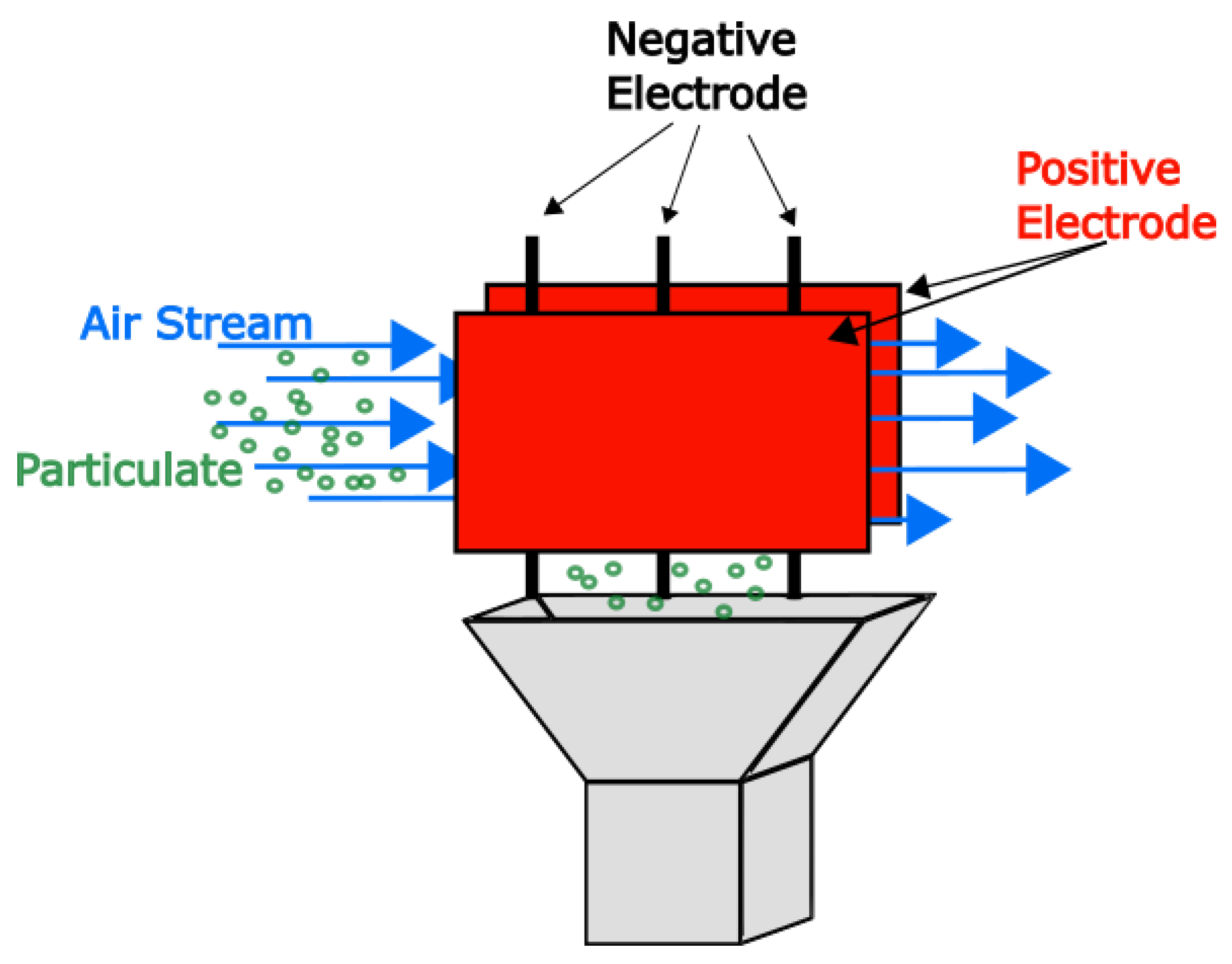
Modern precipitator design is slightly different, as it uses parallel plates instead of the cyclindric chamber as a way to maximize the operating area of the electrode in contact with the gas,
Figure 1. The parallel plates are connected to the ground, acting as the negative electrode, and several bars are placed in the middle of them, acting as the positive electrode, between the bars and the plates, a high voltage is applied, ionizing the gas flow between plates, and the pollutant particles are attracted to the plates, which serve as a collector.
The high voltage is applied constantly to the electrodes, but additionally an alternative working mode is used, the pulse energization mode, presented in [
2] as the most important change in precipitator technology since Professor Cottrell’s patent. It consist of maintaining the precipitator at a reduced DC voltage, and superimposed with this voltage, a repetitive high voltage pulse train is applied. This method is typically used in the paper industry, cement kilns, coal fired power stations, etc., as it improves in the separation of certain particle types like high resistivity ones.
ESPs stand as one of the most feasible solutions, having a high effectiveness, and this solution become very attractive when taking into account the low interference with the gas flow rate in comparison with other methods which use a physical barrier affecting the gas propagation speed, as well as the cost and the easy maintenance [
2].
2. The High Voltage Converter
For the precipitator operation, the high voltage range typically goes from some kV to 12 kV, however high ranges can also be found. To obtain this voltage from the AC grid, a step-up transformer must be used due to the voltage boost needed but also for security reasons, due to high voltage hazards. Typical isolated topologies have some power limitations, and Flyback is recommended for power ratings up to 200 W for discontinuous mode and 250 W for continuous mode, Forward topology is recommended for a 250-W and 500-W power rating in case of a single transistor and double transistor respectively. In case of push pull or half bridge topologies, the power rating is limited also to 500 W [
4,
5]. If the foreseen power output is in the range of kilowatts, it is better to think two or three legs full bridge inverter. For this application a two-leg full bridge converter is more suitable because there is no need for a three-phase system to feed a high voltage transformer and the rest of the elements. A resonant converter offers an interesting option due to its ability to control the voltage output with the switching frequency using a minimal component count [
6]. The power efficiency obtained by them also becomes an aspect to investigate, as nowadays power saving is a big issue that is directly related with particle emissions from power plants that still use fossil fuels in energy production.
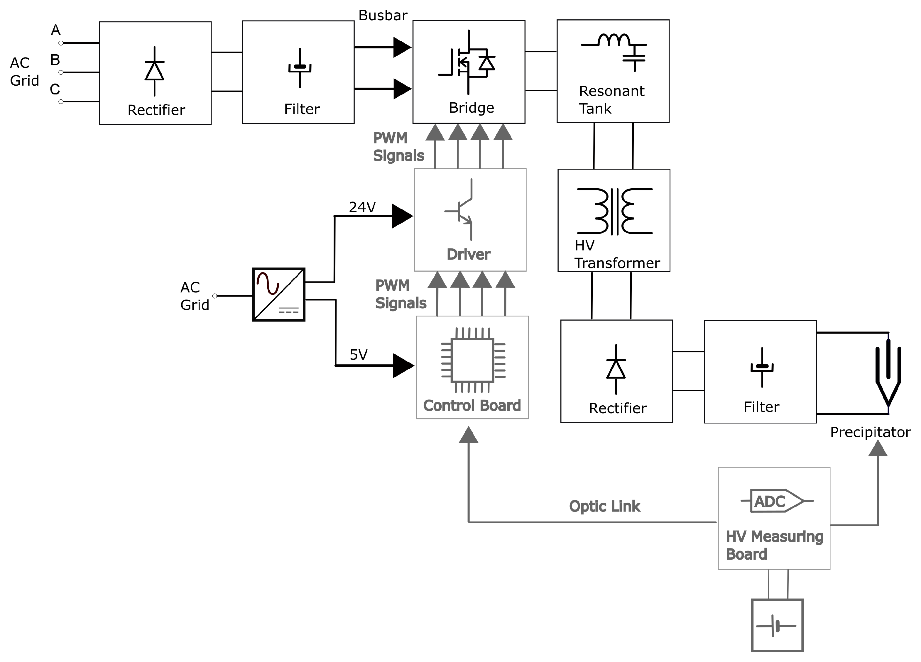
The proposed block diagram is shown in
Figure 2. The AC grid is rectified and filtered to feed the full bridge though the busbar, outside the bridge the resonant circuit and the high voltage transformer are located.
At the transformer output, a square wave voltage is expected, which has to be rectified and filtered, with the filter output feeding the precipitator. The blocks in light gray are the elements of the control part, and in the center the microcontroller is located, which generates the firing signals for the full bridge, according to the user commands. Those signals are carried to the driver which can adapt them in power and shape to a more suitable signal level considering the type of power switch used, MOSFET or IGBT, providing the complete charging of the gate parasitic elements, and abrupt gate voltage transitions. Another important element in this part is the high voltage measuring board, as its useful to have a mean to measure the system output and pass this information to the microcontroller. For security reasons this part must be completely isolated from the rest of the system, particularly from where the user is close to the control board. To isolate this board, an optical link is proposed, and to avoid the use of another isolated DC/DC this part will be battery powered.
2.1. The PRC
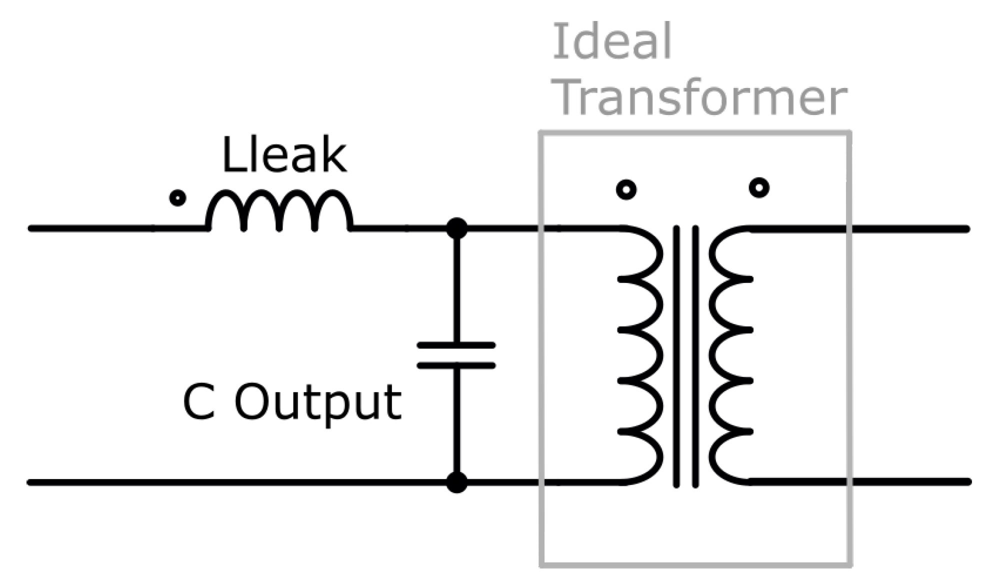
The selected topology is the Parallel Resonant Converter (PRC) because some of the components needed in the resonant tank are already present in the equivalent circuit of the step-up transformer when considering the parasitic elements,
Figure 3. The PRC main element is the resonant tank, composed by a series inductor
with a parallel capacitor
,
placed as a filter capacitor. The resonant tank output voltage is managed through the switching frequency, the phase between inverter legs firing gate, and is also defined by the step-up transformer winding ratio.
The analysis of the converter was carried out in [
7] using base parameters, that is a normalized analysis, where
and
are calculated from
and
elements. First we define the base parameters as the base voltage:
The base impedance impedance relates the L and C of the tank circuit:
Then we define the normalized parameters, normalized omega:
normalized resistance, relating the L and C of the tank circuit:
Finally the voltage and power is shown as:
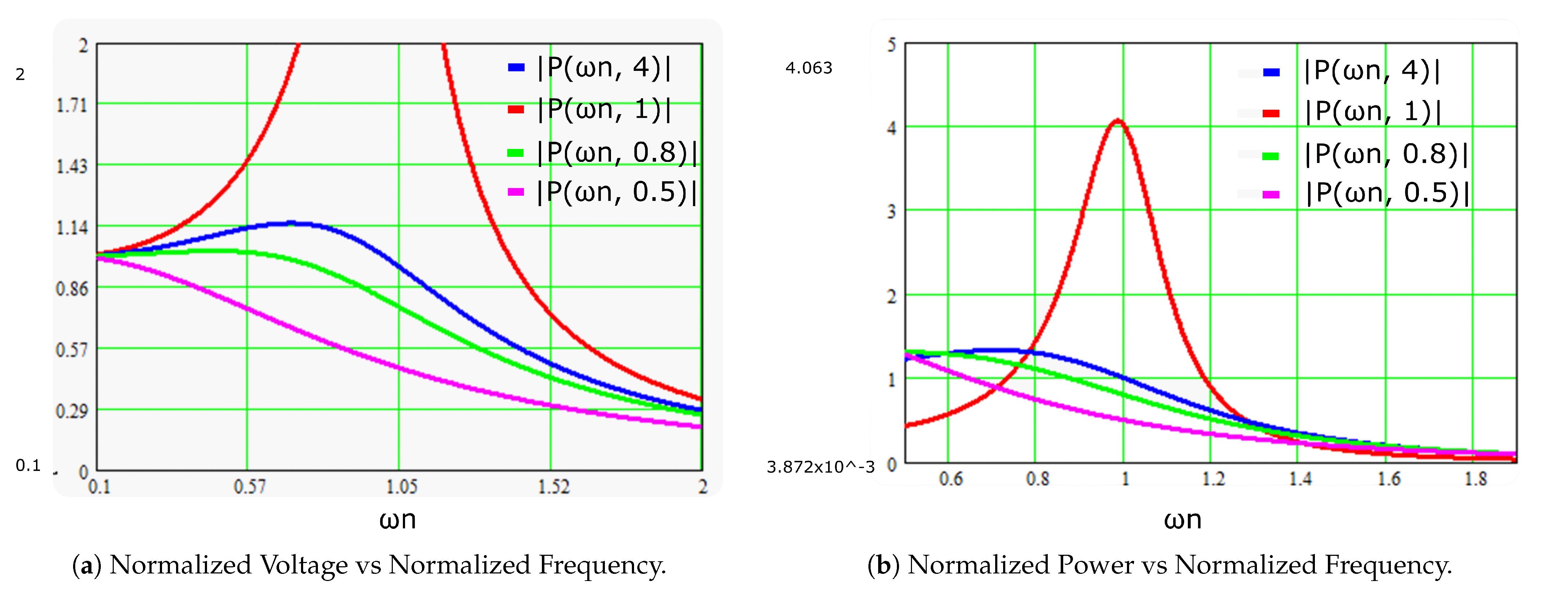
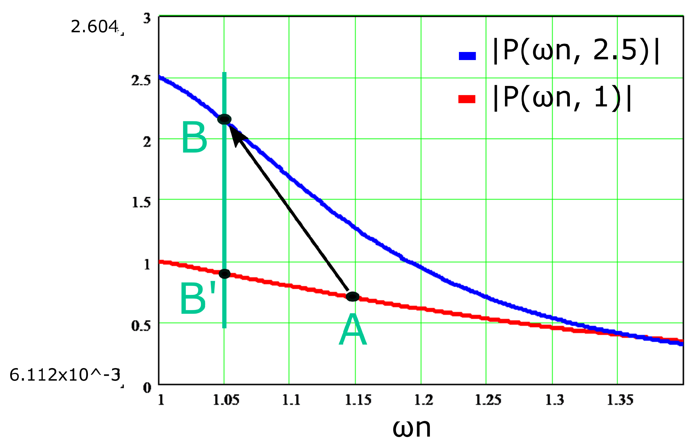
The resonant converter usage is also justified by the implementation of the pulse energization method. Constant output can be regulated as mentioned earlier, by the converter switching frequency and phase shift, the pulsed output can be implemented acting on the resonant tank components, reducing the inductor value in a controlled manner by some electronic method, which will increase the inverter output. The graphs of
Figure 4 and
Figure 5 are obtained using the first harmonic approximation, they are useful to observe the converter trend, if the frequency is modified by how it affects the normalized impedance. If
is changed the output power also changes, for a normalized output load of 1, a change in normalized
from 1.2 to 1.1 as shown in
Figure 5 (point A to B’), the output power variation goes from 213 W to 233 W. If the series inductor
changes, it implies a change in
(Equation (
3)) and
(Equation (
4)) and therefore in
, changing from point A to B, the output power variation goes from 213 W to 553 W.
At the same time, the power will be higher because the normalized impedance is now lower, which increases the power transfer capability. This can be explained with the help of
Figure 5. From the initial operation point A. This correspond to the variation of point A to point B’. The power increase is even higher because the value of the output normalized load also changes (
6). The new value corresponds to point B.
2.2. The Variable Inductor
The inductor, which allows the power variation described in the previous section, is based on the variable inductor theory [
8,
9,
10,
11,
12]. The variable inductor operation is based on the change of the operating point within the B-H Curve of the magnetic material. This change is possible, injecting a DC current into an auxiliary couple of windings. Using a double E core with the main winding connected to the resonant tank in series with the transformer leakage inductance and a couple of auxiliary windings in the external arms used to inject an external DC, it will make the total series inductance vary. The inductor E core has a reluctance dependant to
which is dependant on the injected DC.
The reluctance is defined as:
where
is the magnetic path length,
is the core cross sectional area, and
is the magnetic permeability.
3. Prototype
3.1. The Inverter
Following the diagram in
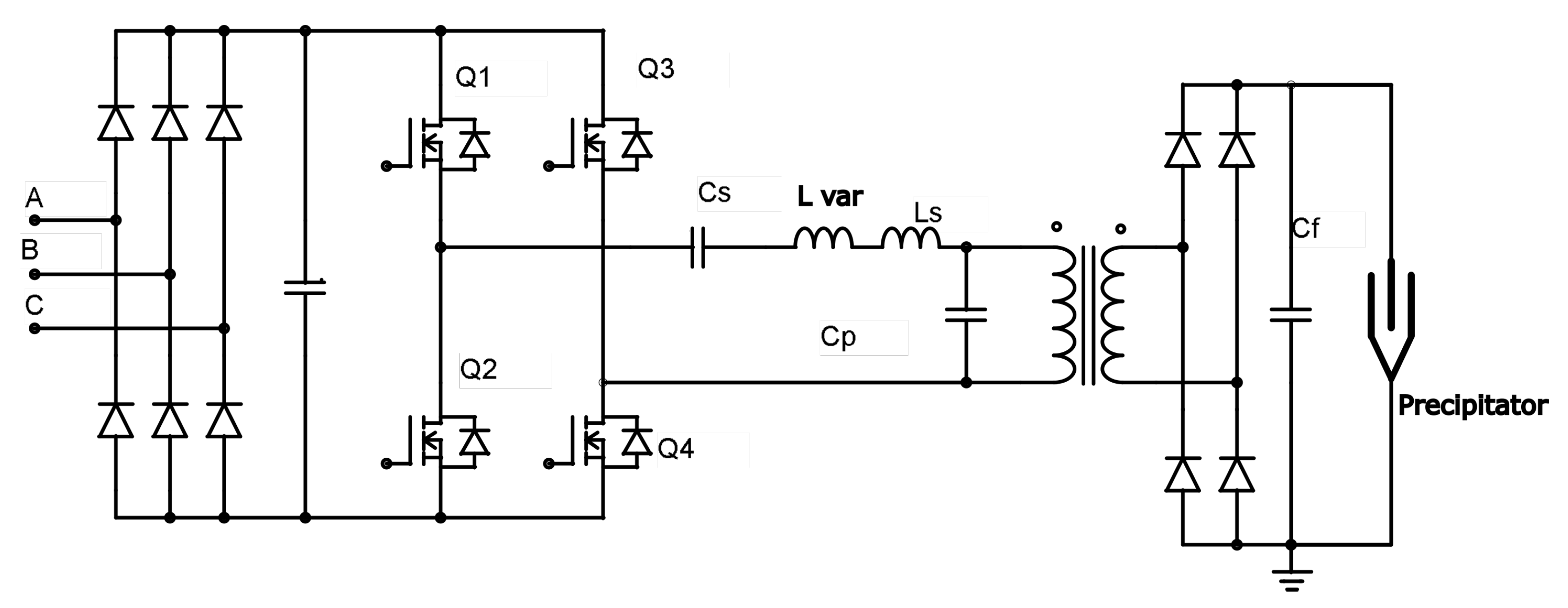
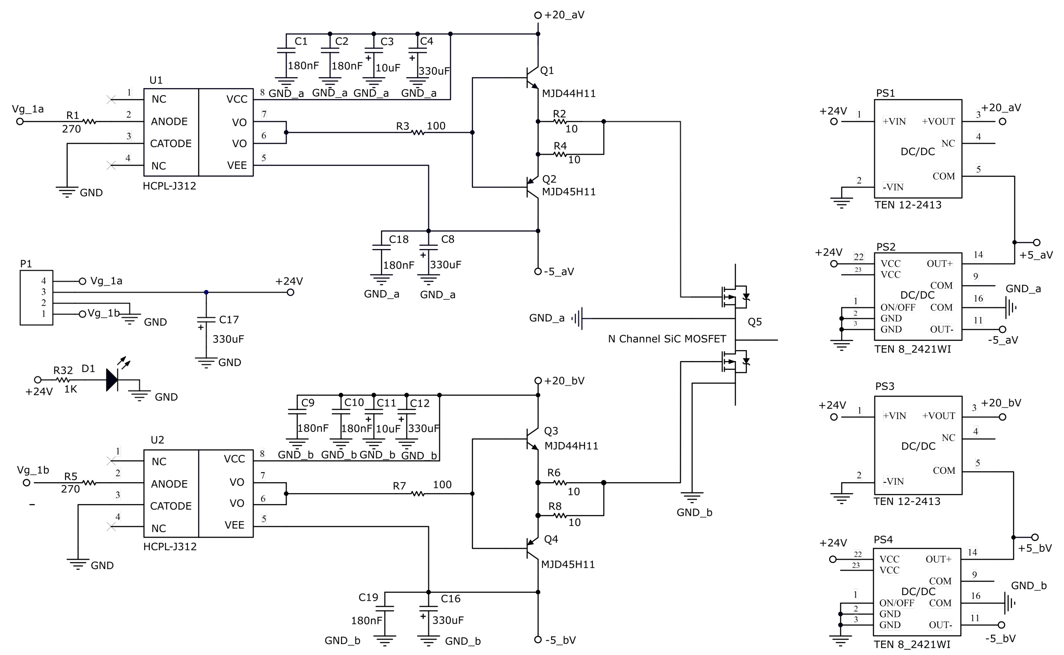
Figure 2, the inverter is composed by the blocks in a dark color, and the block rectifier, filter, bridge, resonant tank, HV transformer, rectifier, and filter are implemented as the schematic of
Figure 6. The rectifier is contained into a single encapsulated component, in the reference 160MT120KPBF from the manufacturer Vishay, the MOSFETs reference is SKM350MB120SCH15, from the manufacturer SEMIKRON, this reference is composed by two MOSFET units, which can be connected in series forming a leg of the inverter. Components of the resonant tank are summarized in
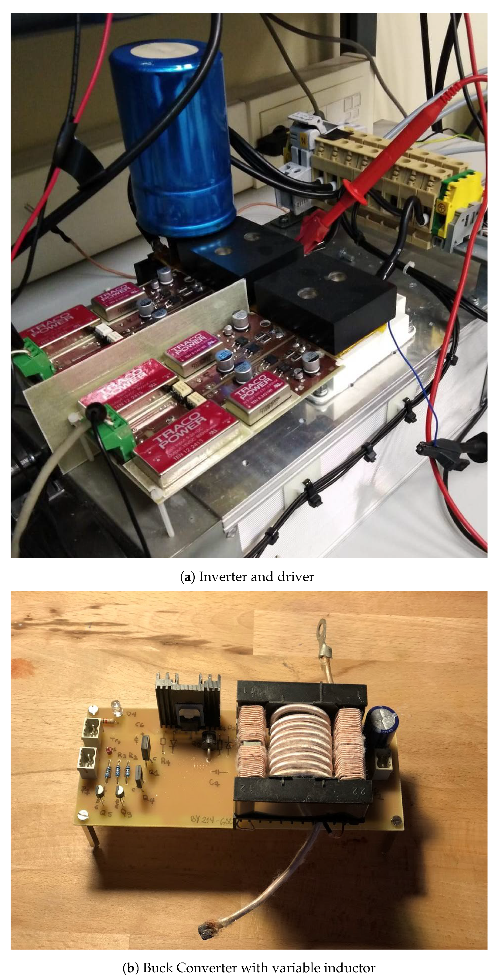
Table 1 Ls and Cp are the parasitic elements of the transformer. L var is the variable inductor added in series with the transformer. The final Inverter assembly is in Figure 17a.
3.2. The Driver
To accomplish those features, an adequate driver must be used,
Figure 7 and Figure 14, a driver capable of supplying the voltage levels to turn on and off a SiC MOSFET, completely discharging the gate parasitic capacitance but also with a good isolation between control signals and the half bridge output for security reasons. The switching pulses output by the driver are +15 V during
and −5 V during
, obtained from two isolated DC/DC converters. Inside the driver board, the component acting as the the driver itself, is an optocoupler HPCL-312, capable of providing enough isolation to the control signals and fast enough to obtain abrupt square waveforms. The optocoupler output is reinforced with two bipolar transistors placed in push-pull configuration to obtain even bigger gate currents.
3.3. The Pulsed Output Unit
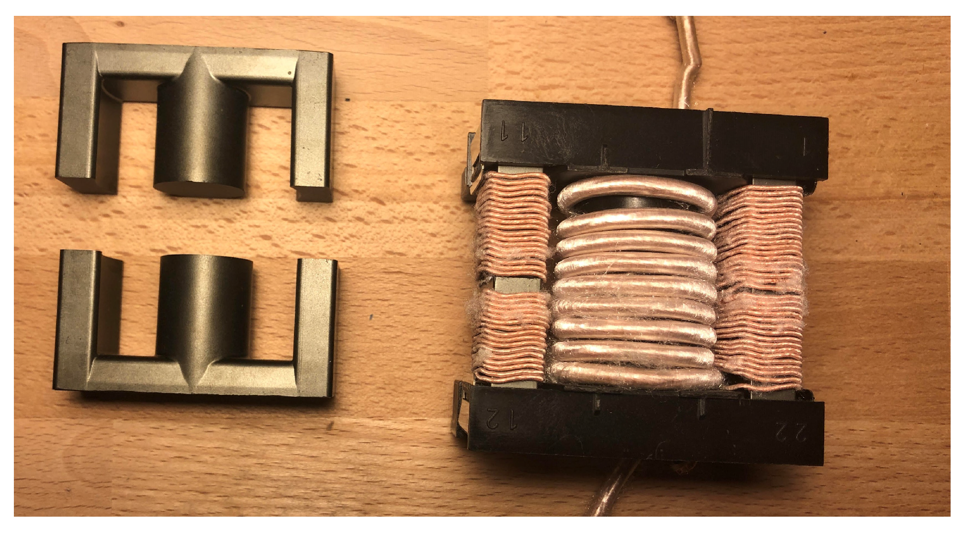
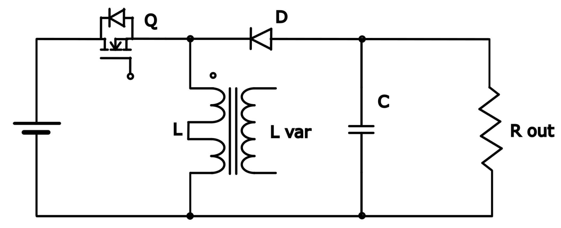
To operate the precipitator in pulse energization mode, the converter output must be kept at a reduced voltage and periodically increase this voltage in a pulsed shape. The pulses are achieved by changing the value of the variable inductor, i.e., injecting a DC into the auxiliary windings of the variable inductor. To do this the inductor was built with an ETD54 core,
Figure 8, with an air gap, the center leg is connected to the resonant tank, named as L var, the auxiliary windings are placed in the core outer arms and connected to a buck converter,
Figure 9 and Figure 17b, acting as the converter inductor. If this converter is loaded with relative small resistance, the output current can be increased and the inductor current, the current regulation in the auxiliary winding can be done changing the buck converter duty cycle, operated also from the control board. Programming a jump in the duty cycle, the buck current experiment has a jump too, and consequently the inductor value of the resonant tank.
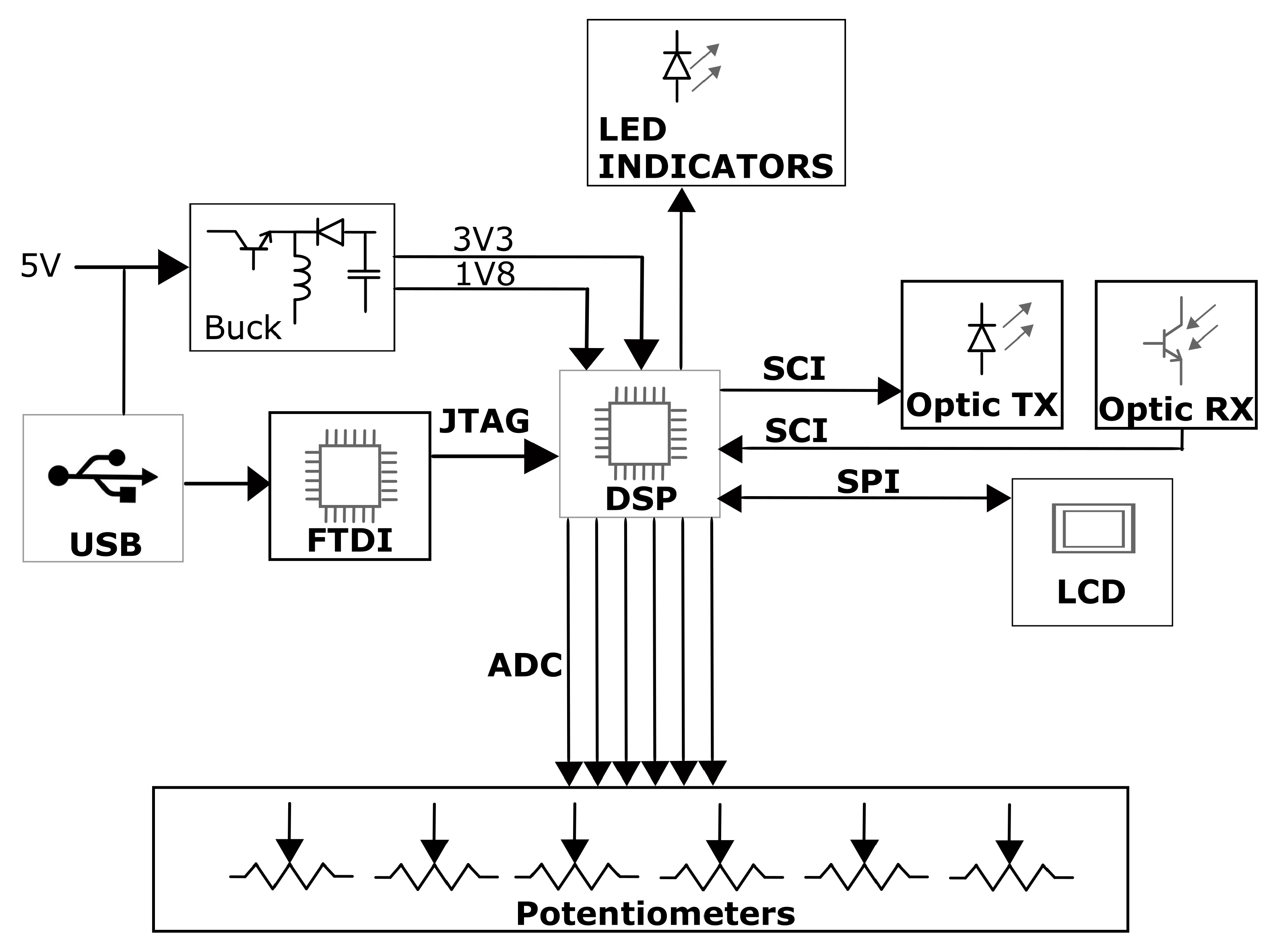
3.4. The Control Board
In the control part, first we have to select the controller. From the 8-bit microcontrollers to the fastest FPGA, many options are available from the semiconductor manufacturers, for this application, the 8- or 16-bit families were discarded, because they might have some limitations in the control loop or in floating point operations. However, the most advanced processors like ARM or FPGA might be more suitable for video processing, automotive infotainment systems, or radio frequency analyzers. In case of industrial applications like robotics, motor control, or inverter control, the better choice is the Texas Instruments (TI) C2000 MCU family, specifically the TMS320F28335 model. The C2000 MCU family is based on the C28x core, a 32 bit CPU in a modified Harvard Architecture microcontroller [
13], suitable for real-time control and digital signal processing. For this application PWM modules must used. The PWM modules [
14] EPWM1 and EPWM2 are associated with two inverter legs and every module has two signals (A and B), one to switch the upper MOSFET in the bridge and the other to switch the lower MOSFET. The third module EPWM3 are used to control the buck converter for pulsed energization.
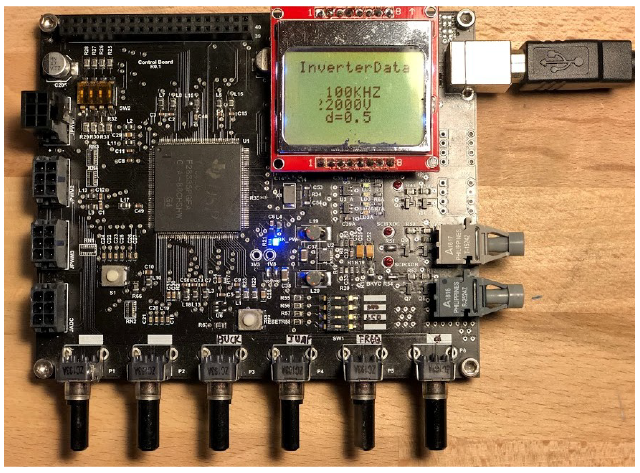
Once selected, the microcontroller family, an adequate platform for the prototype must be explored, something which enables firmware programming, testing the microcontroller peripherals, running speeds, LCD refreshing, etc., for that purpose it might be very useful that any of the development boards offered by the manufacturer TI. The selected development board for the first prototype was the TMS320F28335 experimenter kit, equipped with the daughter card containing the mentioned microcontroller and a prototyping area in which some external circuitry can be added. As the design advance, the program is getting bigger and the prototyping area busier, with almost no remaining space for more modifications, with a mess of wires, making it difficult to follow the electrical connections, but also more important, with poor robustness of the system, particularly if the frequencies are increased. For those reasons, the initial development board was changed for a new custom made PCB, Figure 11. The block diagram of this PCB is represented in
Figure 10.
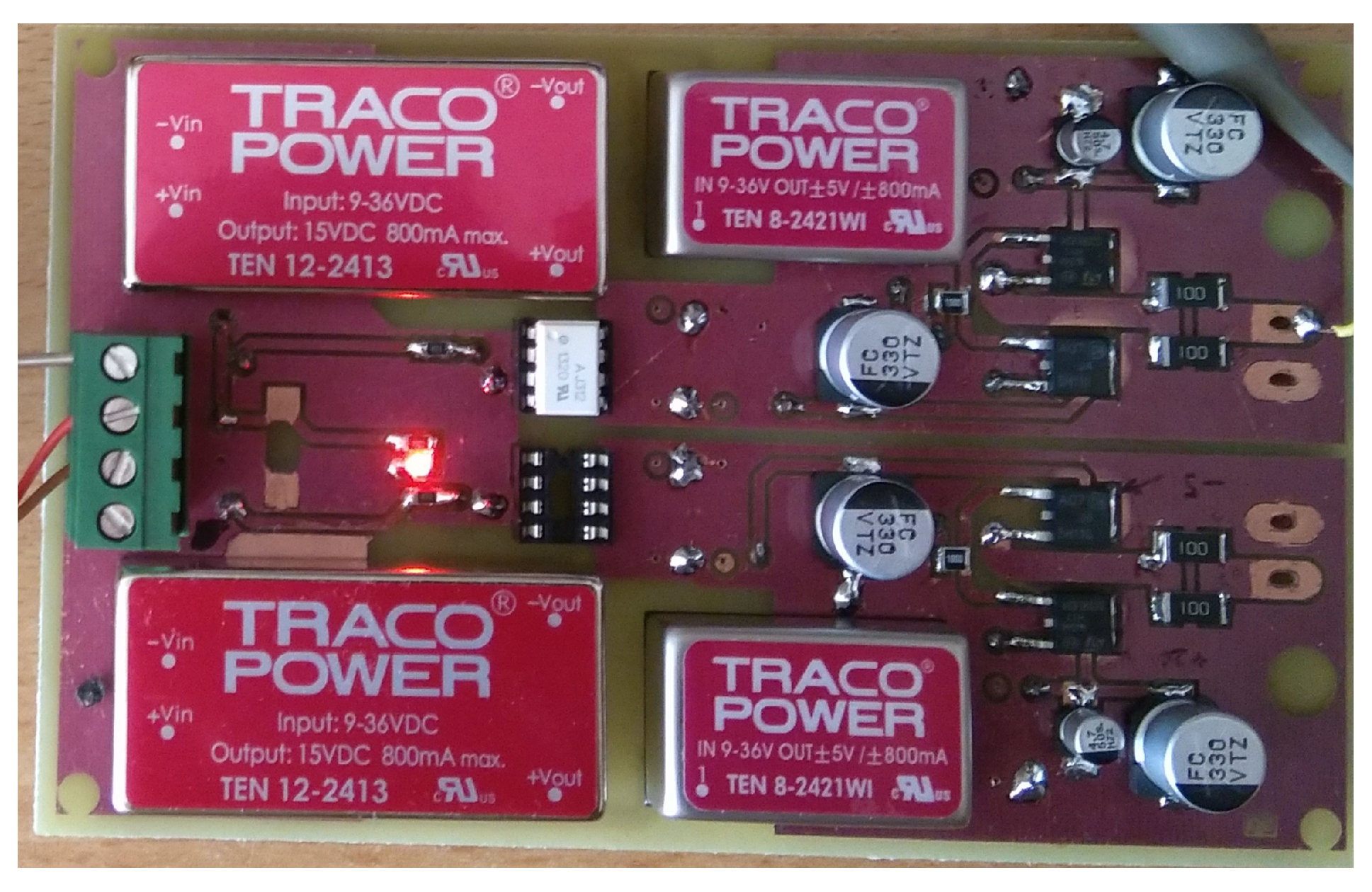
The control system has two DC main buses, one for the digital circuits inside the board and the other for the external drivers. The digital DC bus could be supplied by an external power supply or by the USB port. Both ways apply 5 V to the board, which converts into the typical 3.3 voltage and 1.8 volts needed by the microcontroller core. For that purpose the TPS62400 IC was used, which is a dual buck converter circuit, also used by TI in some daughter cards which employ the F2833x family. This IC has a current capability of 400 mA for the 3.3 V output and 600 mA for the 1.8 V output, it integrates inside the same chip the two converters, making it easier for PCB routing and shortening the distance between the buck MOSFETs and inductors.
As explained earlier, an isolated communication is needed in this system. The DSP serial port (SCI) is connected to a versatile link transmitter and receiver fiber optics from the manufacturer Avago. This board has a simple human machine interface, designed to interact with the converter but also offering flexibility to design several experiments to develop in the laboratory. The user command signals are introduced by several potentiometers attached to the ADC, and parameters like frequency, phase shift, or high voltage output are shown in a small graphic display.
The board is equipped with a small LCD to show different inverter parameters during the experiments, which helps the user to know how the system is working. The parameters are:
The LCD selected is the one used by the popular Nokia 5110 cell phone, although the phone is no longer manufactured, its LCD has become very common nowadays in experimenter boards. This LCD is based on the controller PCD8544, which offers the possibility to communicate with the main controller by a SPI port. The instructions used to communicate with the LCD are quite simple, data is sent by the SPI port, setting the DC pin for data sending, and resetting the DC pin for command sending.
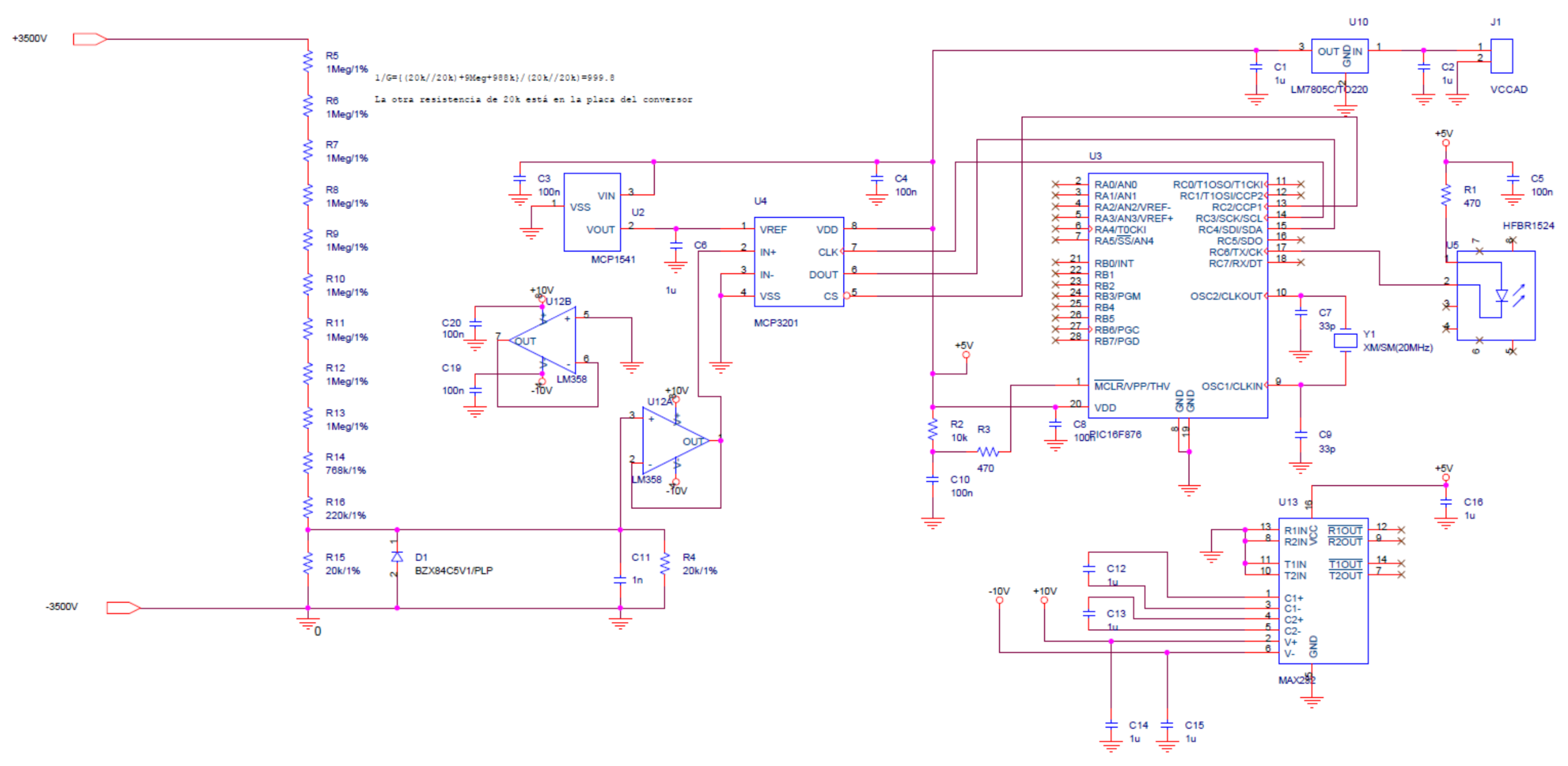
3.5. The High Voltage Measuring Board
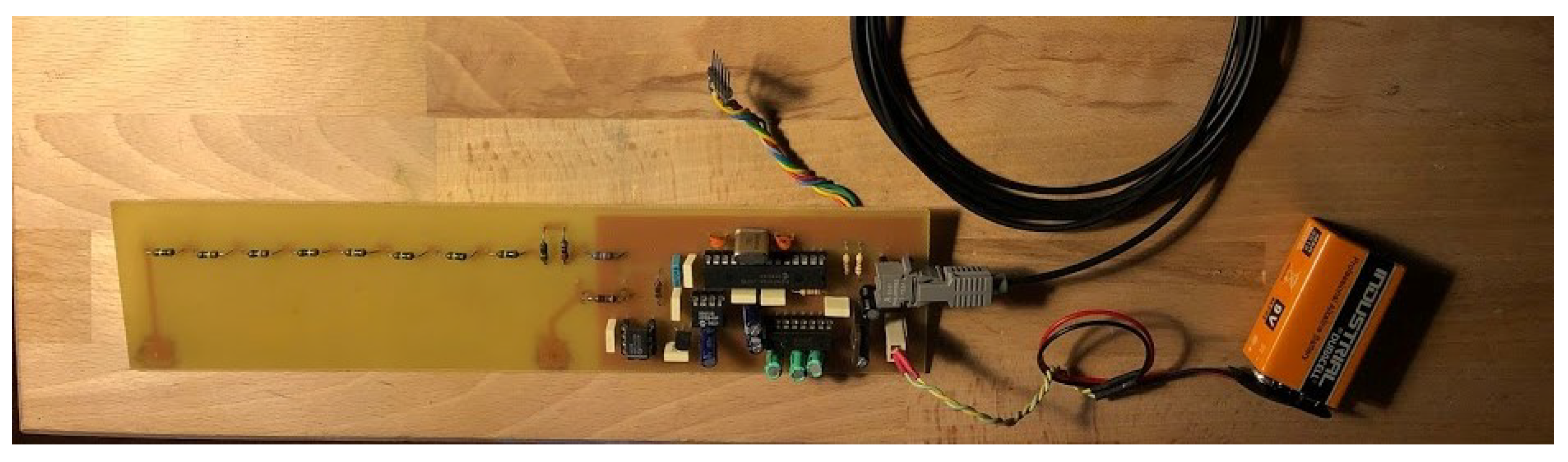
To control ESP, the converter output voltage must be controlled. To do that, the microcontroller needs to measure the converter output voltage in a secure manner. A direct way to measure the output voltage is with the microcontroller ADC, however in this study it is discarded for security reasons, considering that we are operating with high voltage values, which is mandatory some kind of isolation, so one possible solution is a direct measuring with a separated board connected with an optical link to the main processor, the schematic of this board is in
Figure 11 and the PCB in Figure 15. This board is designed with its own microcontroller, a PIC18F2550, powered by a 9 V battery. Using a resistive divider with a voltage follower and a SPI ADC connected to the PIC, it its possible to measure the high voltage by the microcontroller, then using its UART, the data can be sent by serial port. This board uses the method of the bleeder resistor, and was used on [
15], and a similar system with resistive voltage divider was also used in [
16], where the effects of the stray capacitance and temperature were compensated.
4. Results
The experimentation parameters were summarized in
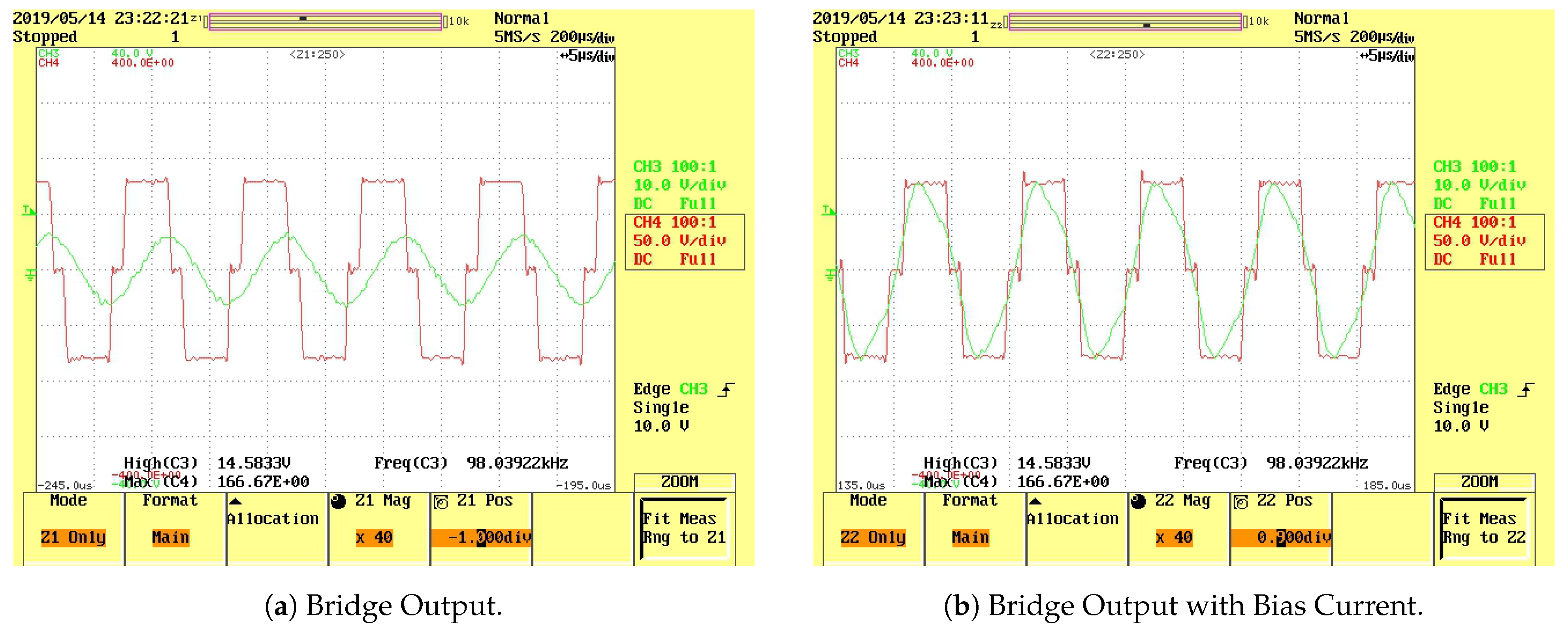
Table 2. First, we start with a 0 bias current and a fixed switching frequency of 98 kHz, which gives us an output of 3 kV on a load of 47 K
. The bridge output current and voltage are shown in
Figure 12a. The red curve is the voltage and the green curve is the current. When a DC current is applied to the bias winding of the variable inductor, the inductance of this inductor lowers and the current rises, as shown in
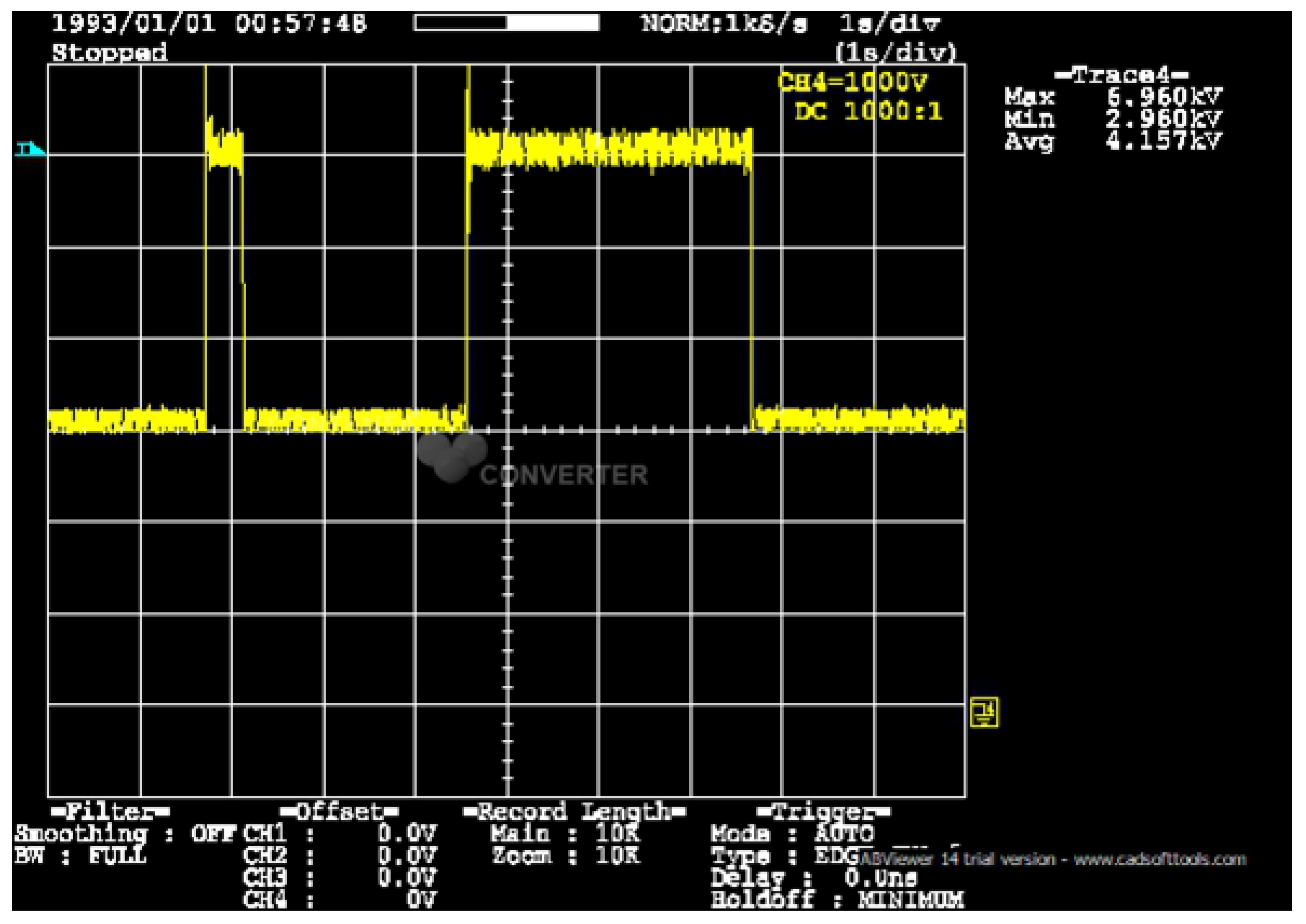
Figure 12b. This reduction of inductance leads to the output voltage to change from 3 to 6 kV, as shown in
Figure 13. The total output power when bias is applied was 768 W. In the figure, two pulses are applied, testing different pulse duration, as a result two high voltage pulses can be observed.
5. Discussion
In this work, a platform for experimenting with high voltage inverters was presented, focused on generating voltage levels and pulses needed to operate a precipitator. Future work on energy efficiency may be done, considering the possibilities of the inverter to operate in ZVS and the good behaviour in frequency losses of the silicon carbide MOSFETs used. Another important aspect to research is the possibility to increase the high voltage output, the inverter has the capability to operate with voltage levels higher than 6 kV and the variable inductor can be redesigned to be operated with less bias current, changing the air gap value.
6. Materials and Methods
The most relevant components are listed then:
TMS320F28335: DSP is TQFP Package;
FT2232D: USB JTAG Debug;
R2524Z: fiber optic receiver;
T1524Z: Fiber optic Transmitter;
PCD8544: LCD Integrated Controller;
TPS62400: Dual buck converter for control board voltages;
ETD54/28/19 Core for variable inductor;
PIC18F2550: microcontroller for the high volt Measuring board;
SKM350MB120SCH15; Silicon Carbide MOSFET;
160MT120KPBF: 3ph rectifier.
7. Conclusions
This work proposed a control system for an electrostatic precipitator through a resonant converter, using one of the most advanced DSP’s available from Texas Instruments. A custom PCB was made, including the DSP, and several output ports. This board enables the implementation of frequency control to adjust the converter high voltage output, but also the pulsed operation mode can be used, having a continuous high voltage output and increasing it periodically in a pulsed shape. The inductor present in the resonant tank was built with additional bias windings used to change the operating point of the converter with the help of a small DC/DC buck converter, making it possible to control the pulsed output from the microcontroller. To measure the converter output voltage, the control board was equipped with a fiber optic communication bus, enabling the use of a high voltage measuring board. The control board has two potentiometers to adjust the frequency and phase shift in the present work but is also open to add more control inputs in future experiments with another four potentiometers. The converter was built with SiC MOSFETs, designing a specific driver for them, and in future work the efficiency offered by this semiconductor can be evaluated. The power variation achieved at 98 kHz with the variable inductor is from 191 W to 765 W. EMI compliance is very complex in power inverters, in the presence of a pulsed energy source wires and PCB tracks become unintended antennas, transmitting at different frequencies. In the radio spectrum, some emissions are easy to predict but others are not. The operating frequency will appear in the EMI graph together with many other frequencies, which are difficult to predict, even in case of topologies which use fixed frequency. This difficulty increases if the converter uses a variable frequency. In this application, a method to operate a resonant converter was presented at a fixed frequency in order to improve the EMI behavior.
Author Contributions
Conceptualization, F.J.G.D. and J.D.; methodology F.J.G.D. and J.G.; software, F.J.G.D. and J.D.; validation, A.M.P.; resources, P.J.V.; writing—original draft preparation, F.J.G.D. and J.G.; writing—review and editing, F.J.G.D. and J.D. All authors have read and agreed to the published version of the manuscript.
Funding
This research was funded by Ministerio de Economía, Industria y Competitividad, Gobierno de España: TEC2014-53324-R.
Conflicts of Interest
The authors declare no conflict of interest, The funders had no role in the design of the study; in the collection, analyses, or interpretation of data; in the writing of the manuscript, or in the decision to publish the results.
Abbreviations
The following abbreviations are used in this manuscript:
| ESP | Electrostatic Precipitator |
| ZVS | Zero Voltage Switch |
| SiC | Silicon Carbide |
| TI | Texas Instruments |
| LCD | Liquid Cristal Display |
| ph | Phase |
References
- Harrison, T.R.; Adams, D.; Benett, I.L.; Resnik, W.H.; George, W.; Wintrobe, T.M. Principles of Internal Medicine; McGraw-Hill-Ko¯gakusha: New York, NY, USA; Tokyo, Japan, 1962. [Google Scholar]
- Parker, K. Electrical Operation of Electrostatic Precipitators; IET Power and Energy: London, UK, 2003. [Google Scholar]
- Frederick Gardner Cottrell. Art of Separating Suspended Particles from Gaseous Bodies. U.S. Patent 895,729, 11 August 1908.
- Mappus, S. The Power to Amaze. Power Converter Topology Trends. 2014. Available online: https://www.psma.com/sites/default/files/uploads/files/10 (accessed on 26 June 2021).
- Patel, R. Power Conversion Deign Guide; Unitrode Corporation, Texas Instruments: Dallas, TX, USA, 2001. [Google Scholar]
- Villegas, P.J.; Martín-Ramos, J.A.; Díaz, J.; Martínez, J.Á.; Prieto, M.J.; Pernía, A.M. A Digitally Controlled Power Converter for an Electrostatic Precipitator. Energies 2017, 10, 2150. [Google Scholar] [CrossRef] [Green Version]
- García Díaz, F.J.; Díaz, J.; García, J.; Alberto, M.P.; Prieto, M.J. Fixed Frequency Resonant Converter Controlled With Variable Inductor For Electrostatic Precipitator. In Proceedings of the EPE 2019 ECCE Europe Conference, Genova, Italy, 2–5 September 2019. [Google Scholar]
- Pernia, A.M.; Nuno, F.; Corominas, E.L.; Lopera, J.M. Resonant converter controlled by variable leakage inductance in the transformer (LIC). In Proceedings of the 1993 Fifth European Conference on Power Electronics and Applications, Brighton, UK, 13–16 September 1993; Volume 3, pp. 124–129. [Google Scholar]
- Perdigão, M.S.; Menke, M.F.; Seidel, Á.R.; Pinto, R.A.; Alonso, J.M. A Review on Variable Inductors and Variable Transformers: Applications to Lighting Drivers. IEEE Trans. Ind. Appl. 2016, 52, 531–547. [Google Scholar] [CrossRef]
- Alonso, J.M.; Martínez, G.; Perdigão, M.; Cosetin, M.; do Prado, R.N. Modeling magnetic devices using SPICE: Application to variable inductors. In Proceedings of the 2016 IEEE Applied Power Electronics Conference and Exposition (APEC), Long Beach, CA, USA, 20–24 March 2016; pp. 1115–1122. [Google Scholar] [CrossRef]
- Medini, D.; Ben-Yaakov, S. A current-controlled variable inductor for high frequency resonant power circuits. In Proceedings of the 1994 IEEE Applied Power Electronics Conference and Exposition—ASPEC’94, Orlando, FL, USA, 13–17 February 1994; Volume 1, pp. 219–225. [Google Scholar] [CrossRef]
- Alonso, J.M.; Costa, M.A.D.; Rico-Secades, M.; Cardesin, J.; Garcia, J. Investigation of a New Control Strategy for Electronic Ballasts Based on Variable Inductor. IEEE Trans. Ind. Electron. 2008, 55, 3–10. [Google Scholar] [CrossRef]
- Bormann, F. F2833x Architecture. In Texas Instruments C2000 Teaching Materials; Texas Instruments: Zwickau, Germany, 2010; Available online: https://mil.ufl.edu/4744/docs/TI_DSP/Bormann_book/m36737.pdf (accessed on 26 June 2021).
- Texas Instruments. TMS320x280x, 2801x, 2804x Enhanced Pulse Width Modulator (ePWM) Module SPRU791F. In Reference Guide; Texas Instruments: Dallas, TX, USA, 2009. [Google Scholar]
- Juan, D.; Pedro, V.; Alberto, M.-P.; Martín-Ramos, J.A.; Miguel, A.; Prieto, J. High-voltage DCDC converter lOKV, 600 W with digital output voltage monitoring. In Proceedings of the IAS Anual Meeting 2013, Orlando, FL, USA, 6–11 October 2013. [Google Scholar]
- Yang, C.; Wu, M.; Jian, C.; Yu, J. The Stray Capacitance on Precision of High-voltage Measurement. In Proceedings of the I2MTC 2009—International Instrumentation and Measurement Technology Conference, Singapore, 5–7 May 2009. [Google Scholar]
| Publisher’s Note: MDPI stays neutral with regard to jurisdictional claims in published maps and institutional affiliations. |
© 2021 by the authors. Licensee MDPI, Basel, Switzerland. This article is an open access article distributed under the terms and conditions of the Creative Commons Attribution (CC BY) license (https://creativecommons.org/licenses/by/4.0/).


