
Optimizing Security of Radio Frequency Identification Systems in Assistive Devices: A Novel Unidirectional Systolic Design for Dickson-Based Field Multiplier


Abstract
1. Introduction
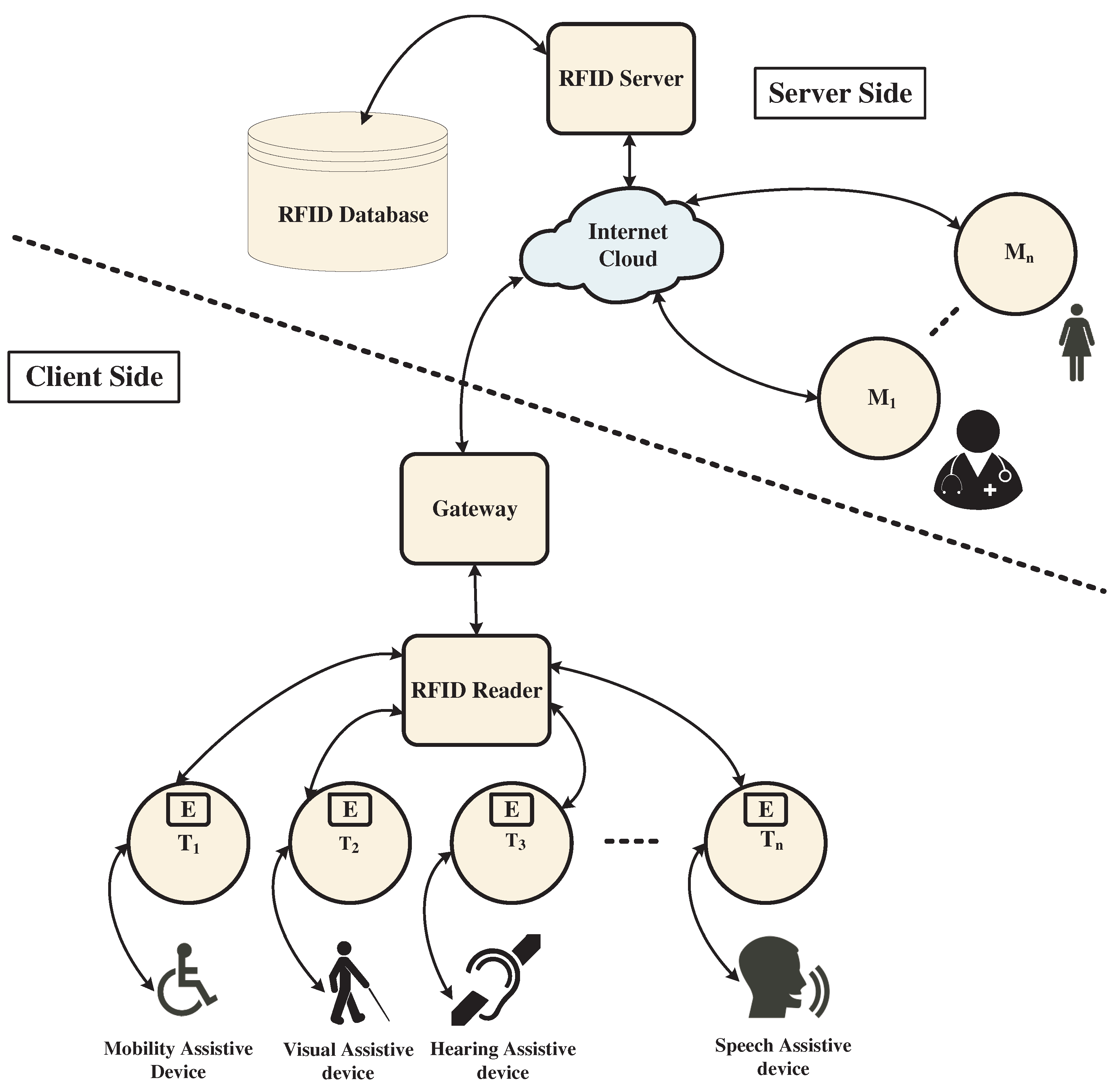
2. RFID-Based IoT-Assistive System
3. Literature Review
3.1. Paper Contribution
3.2. Paper Organization
4. Dickson Basis Multiplier in GF()
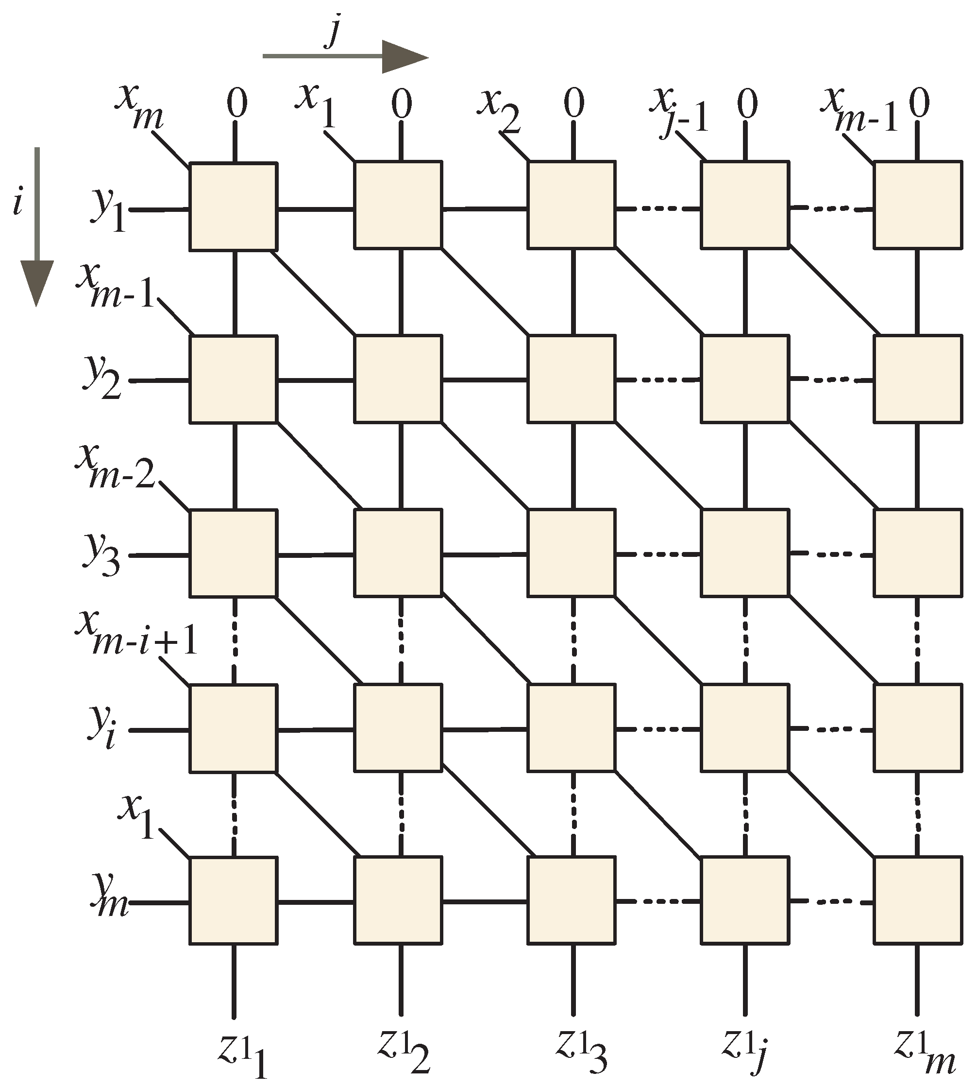
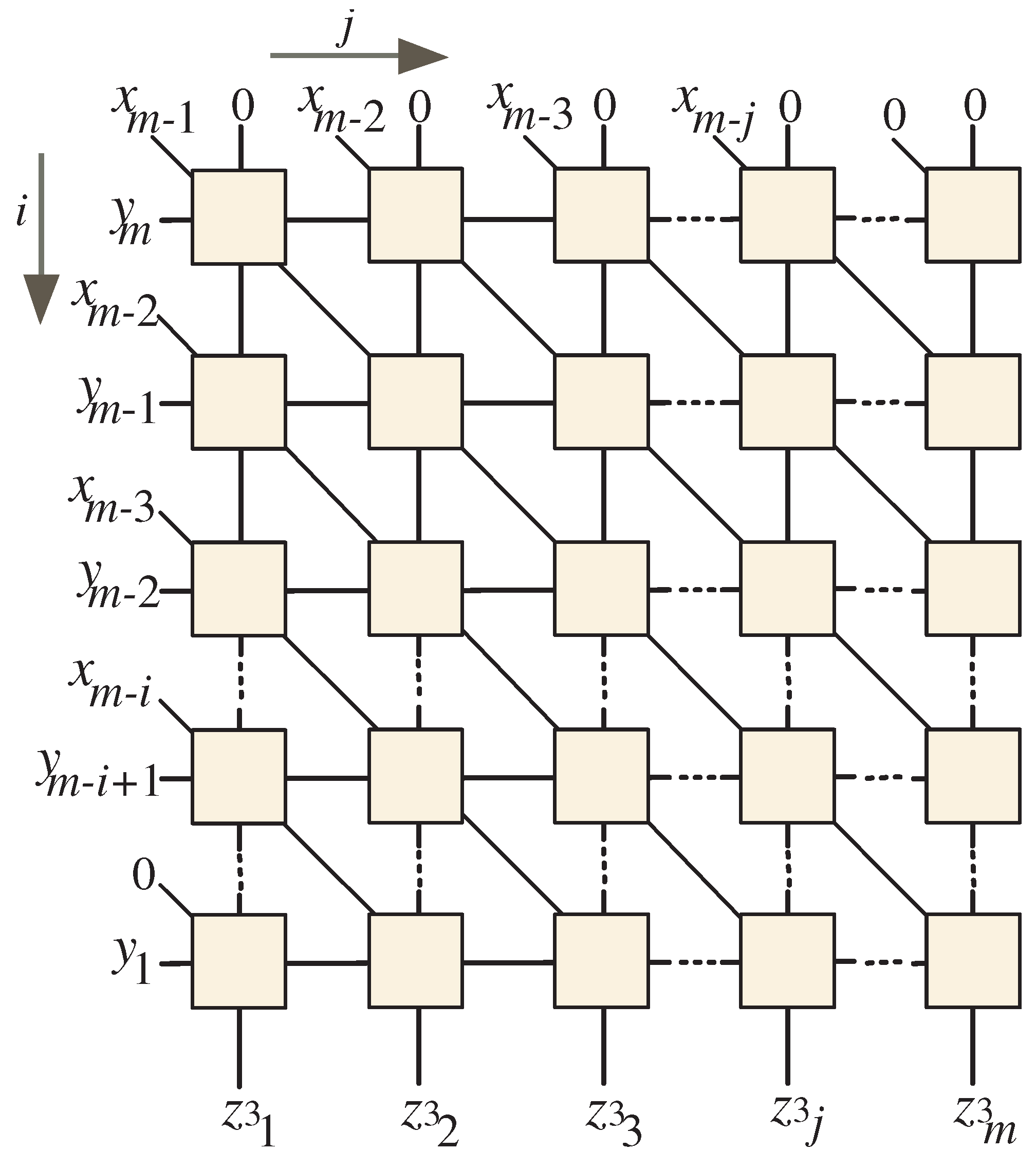
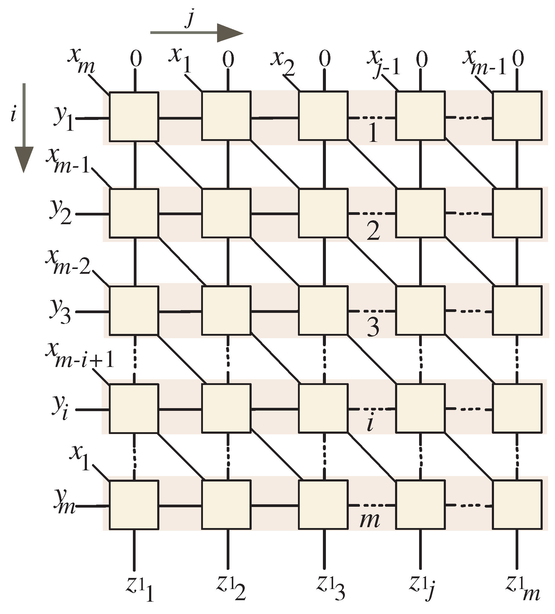
5. Constructing Dependency Graphs
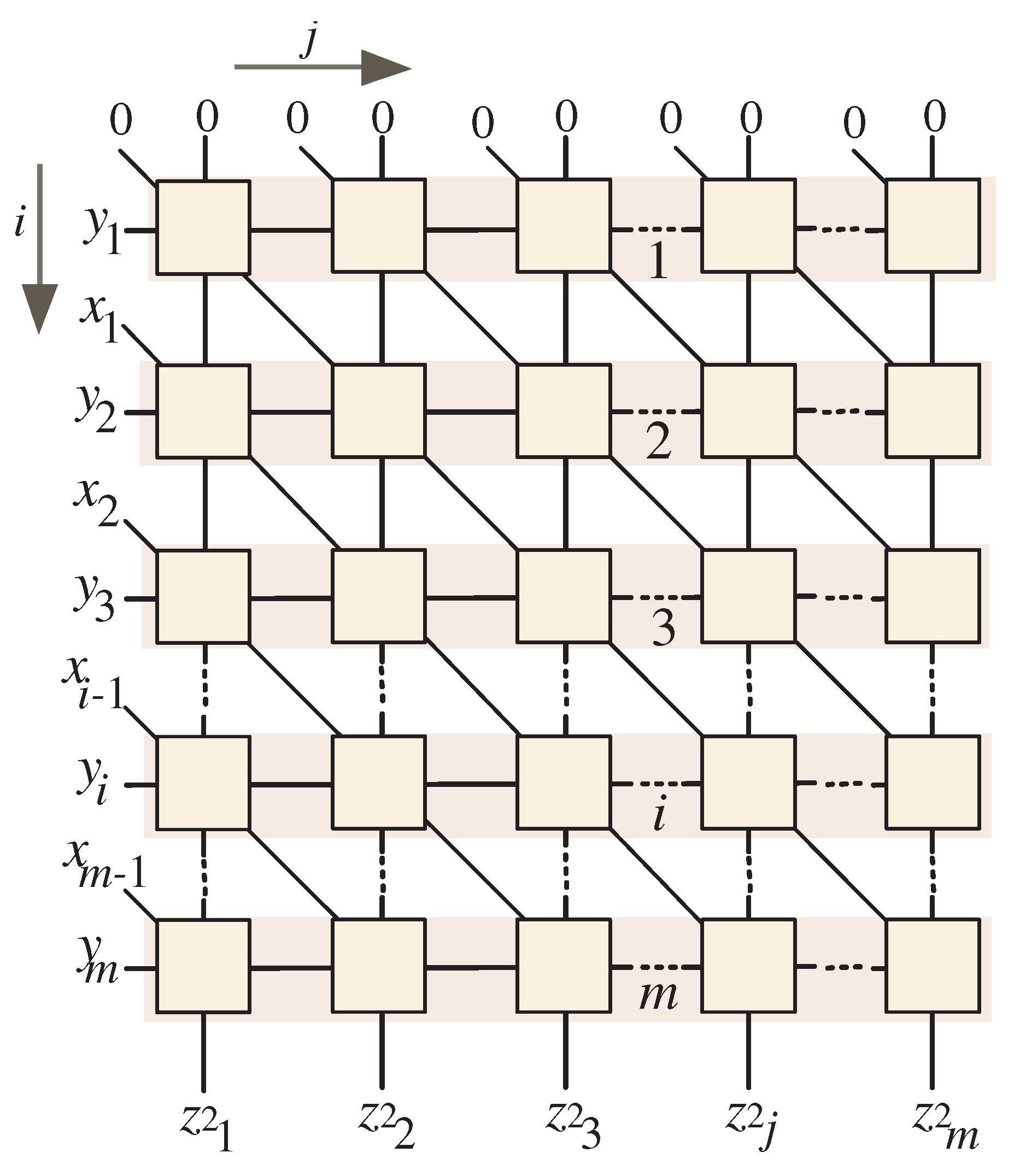
- Horizontal flow: This flow is specifically assigned to the input signals , where . These signals are strategically introduced into the dependency graph (DG) from the left side, ensuring a clear pathway for processing them effectively.
- Top input entry: The top section of the DG serves as the initial input location for the zero values of the signals (, for ). In Section 6, we will provide a detailed explanation of how to properly set up by clearing the flip-flops that control its output, thus preparing the system for accurate computation from the outset.
- Diagonal connectors: The diagonal connectors depicted at the left edges of the input nodes are utilized to incorporate the input signals and , where and . This design choice facilitates the effective integration of these signals into the computation, enhancing the overall functionality of the DG.
- Horizontal flow: This orientation is also designated for the input signals , where . These signals are introduced into the DG from the left side.
- Top input entry: The upper section of the DG serves as the access point for the initial zero values of the signals (, for ). In Section 6, we will detail how to internally initialize by clearing the flip-flops associated with its output at the beginning of the computation.
- Diagonal connectors: The diagonal lines illustrated at the left edges of the input nodes are utilized to incorporate the initial zero inputs of the signal and signal , where and .
- Horizontal flow: This flow is designated for the input signals , where . These signals come from the left side of the DG, facilitating a seamless progression of data.
- Top input entry: The top section of the DG functions as the entry point for the initial zero values of the signals (, for ). In Section 6, we will explain how to set up by clearing the flip-flops that control its outputs at the start of the computation. This step ensures that the system initializes correctly, paving the way for accurate calculations.
- Diagonal connectors: The diagonal connectors illustrated at the left edges of the input nodes are employed to input the coefficients of the signals and , where . It is essential to highlight that the coefficient input is consistently set to zero, which is vital for maintaining calculation accuracy.
6. Unidirectional Dickson-Based Systolic Multiplier Structure Construction
6.1. Scheduling Function
6.2. Projection Function
6.3. Extracting the Unidirectional Systolic Multiplier Design
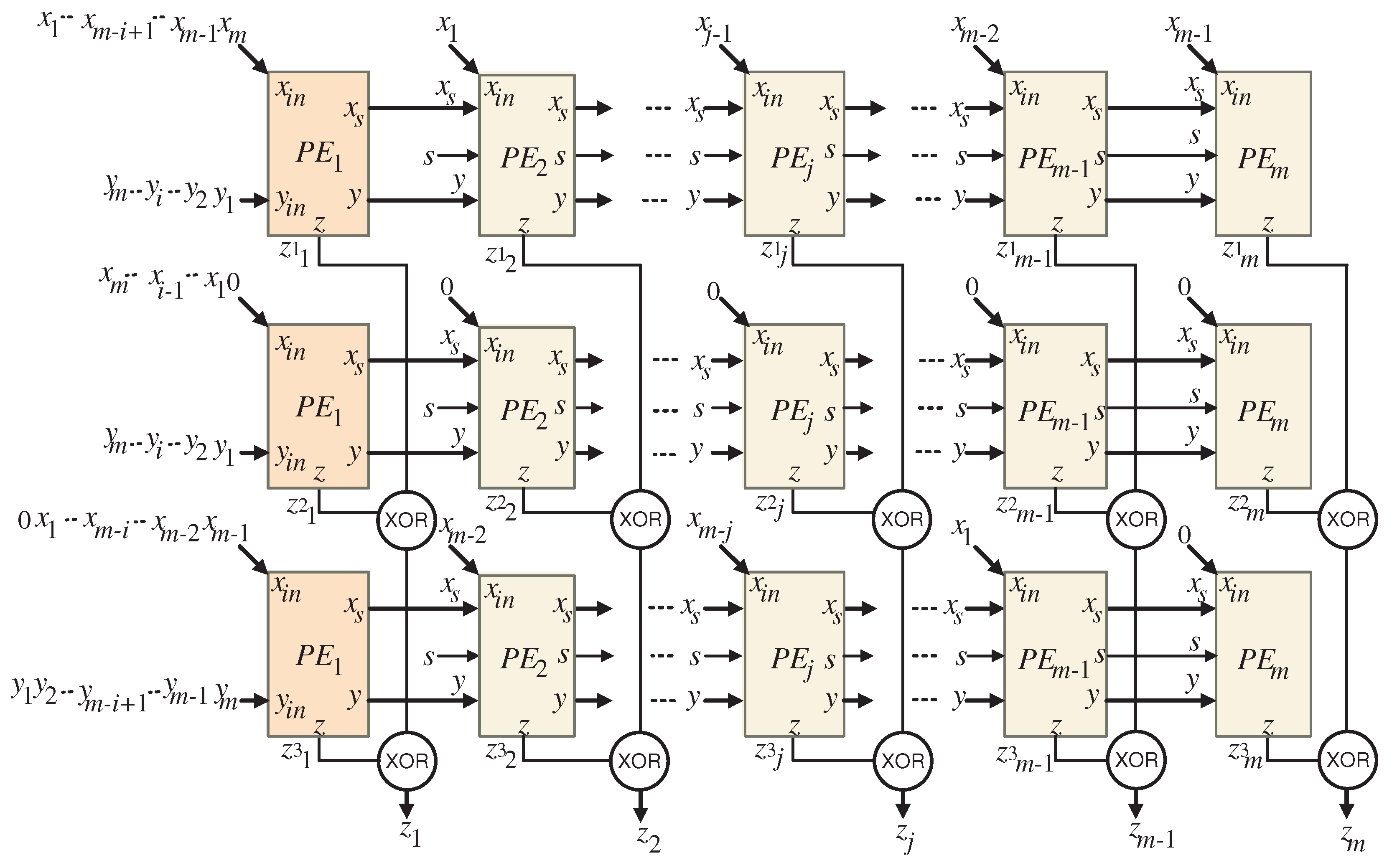
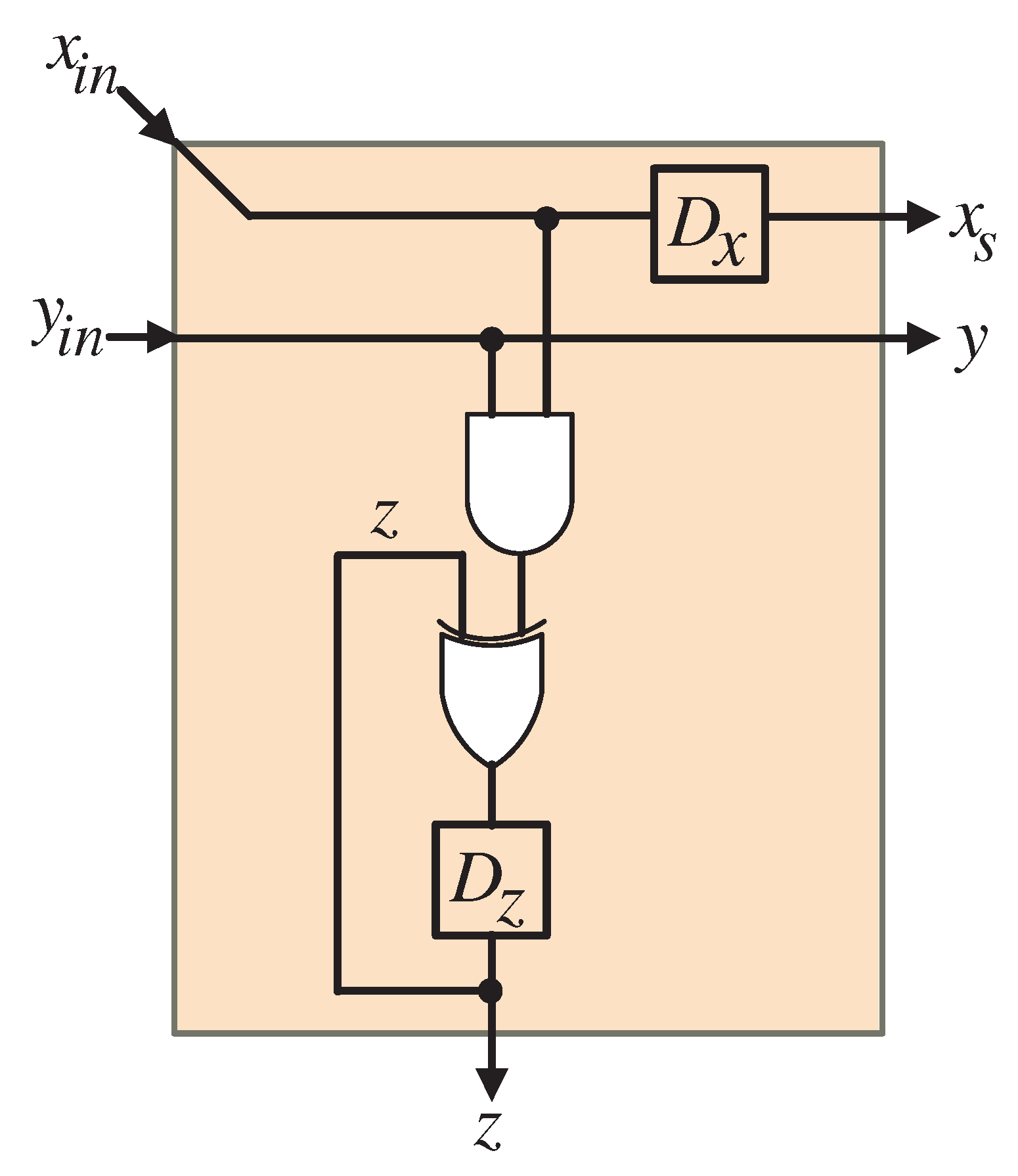
- Setup: In the first clock cycle, the latches illustrated in Figure 9 and Figure 10 are cleared, resulting in the coefficient bits z being initialized to zero. This crucial step eliminates any previous data, preparing the system for fresh computations. Simultaneously, the control signal s is enabled (), which facilitates the flow of input signals assigned to the port —specifically , 0, and , for —through the top tri-state buffer shown in Figure 9. This ensures that the signals are accurately routed to their respective PEs. Additionally, during this clock period, the initial bits of the signals , , and (for ) are introduced to the appropriate first PE (PE1) in each systolic array via the port depicted in Figure 10, initiating the computation process.
- Processing: From the second clock cycle onward, continuing through clock cycle m, the control signal s is turned off (). This change allows the temporary signals to be processed through the standard PEs (), enabling the calculation of values assigned to the z port of the systolic arrays. During these clock cycles, it is essential for the remaining bits of the signals , , and (for ) to be fed sequentially into the appropriate first PE () of the upper, central, and bottom systolic arrays through port . This structured input ensures a continuous and efficient flow of data throughout the system.
- Final Output: At the conclusion of the operation, specifically during clock cycle m, the output bits of the product Z, denoted as (for ), are generated at the outputs of the final row of XOR gates illustrated in Figure 8. This concurrent generation of outputs marks the successful completion of the multiplication process, allowing for immediate access to the results.
7. Results Overview and Analysis
7.1. Complexity Analysis
7.2. Implementation Findings
8. Key Findings and Conclusions
Author Contributions
Funding
Institutional Review Board Statement
Informed Consent Statement
Data Availability Statement
Acknowledgments
Conflicts of Interest
Abbreviations
| RFID | Radio Frequency Identification |
| IoT | Internet of Things |
| COTS | Commercial Off-The-Shelf |
| ADP | Area–Delay Product |
| PDP | Power–Delay Product |
| VHDL | Very High-Speed Integrated Circuit Hardware Description Language |
| ASIC | Application Specific Integrated Circuit |
| ECC | Elliptic Curve Cryptography |
| DG | Dependency Graph |
| CPD | Critical Path Delay |
References
- Semary, H.; Al-Karawi, K.A.; Abdelwahab, M.M.; Elshabrawy, A. A Review on Internet of Things (IoT)-Related Disabilities and Their Implications. J. Disabil. Res. 2024, 3, 20240012. [Google Scholar] [CrossRef]
- Giannakas, F.; Troussas, C.; Krouska, A.; Voyiatzis, I.; Sgouropoulou, C. Blending cybersecurity education with IoT devices: A u-Learning scenario for introducing the man-in-the-middle attack. Inf. Secur. J. A Glob. Perspect. 2023, 32, 371–382. [Google Scholar] [CrossRef]
- Wambui, N. Medical Identification and Sensing Technology for Assisting and E-Health Monitoring Systems for Disabled and Elderly Persons. J. Biomed. Sustain. Healthc. Appl. 2022, 2, 9–17. [Google Scholar] [CrossRef]
- Al-karawi, K.A. Internet of Things (IoT) about Disabilities: Disabilities in relation to the Internet of Things (IoT). ScienceOpen Preprints 2023. [Google Scholar] [CrossRef]
- Ando, B.; Baglio, S.; Castorina, S.; Crispino, R.; Marletta, V. An assistive technology solution for user activity monitoring exploiting passive RFID. Sensors 2020, 20, 4954. [Google Scholar] [CrossRef] [PubMed]
- Shah, S.A.; Fioranelli, F. RF sensing technologies for assisted daily living in healthcare: A comprehensive review. IEEE Aerosp. Electron. Syst. Mag. 2019, 34, 26–44. [Google Scholar] [CrossRef]
- Wang, J.; Pan, C.; Jin, H.; Singh, V.; Jain, Y.; Hong, J.I.; Majidi, C.; Kumar, S. Rfid tattoo: A wireless platform for speech recognition. Proc. Acm Interact. Mob. Wearable Ubiquitous Technol. 2019, 3, 1–24. [Google Scholar] [CrossRef]
- Sula, A.; Spaho, E.; Matsuo, K.; Barolli, L.; Xhafa, F.; Miho, R. A new system for supporting children with autism spectrum disorder based on IoT and P2P technology. Int. J. Space-Based Situated Comput. 2014, 4, 55–64. [Google Scholar] [CrossRef]
- Gilart-Iglesias, V.; Mora, H.; Pérez-delHoyo, R.; García-Mayor, C. A computational method based on radio frequency technologies for the analysis of accessibility of disabled people in sustainable cities. Sustainability 2015, 7, 14935–14963. [Google Scholar] [CrossRef]
- García-Catalá, M.; Rodriguez-Sánchez, M.C.; Martín-Barroso, E. Survey of indoor location technologies and wayfinding systems for users with cognitive disabilities in emergencies. Behav. Inf. Technol. 2022, 41, 879–903. [Google Scholar] [CrossRef]
- Ray, P.P.; Dash, D.; De, D. A systematic review and implementation of IoT-based pervasive sensor-enabled tracking system for dementia patients. J. Med Syst. 2019, 43, 1–21. [Google Scholar] [CrossRef]
- Vrančić, A.; Zadravec, H.; Orehovački, T. The Role of Smart Homes in Providing Care for Older Adults: A Systematic Literature Review from 2010 to 2023. Smart Cities 2024, 7, 1502–1550. [Google Scholar] [CrossRef]
- Jellen, I. Towards Security and Privacy in Networked Medical Devices and Electronic Healthcare Systems. Master’s Thesis, California Polytechnic State University, San Luis Obispo, CA, USA, 2020. [Google Scholar]
- Khan, M.A.; Ullah, S.; Ahmad, T.; Jawad, K.; Buriro, A. Enhancing Security and Privacy in Healthcare Systems Using a Lightweight RFID Protocol. Sensors 2023, 23, 5518. [Google Scholar] [CrossRef] [PubMed]
- Miniaoui, S.; Muammar, S.; Lubamba, C.; Fachkha, C. Comparing cyber physical systems with RFID applications: Common attacks and countermeasure challenges. Int. J. Bus. Inf. Syst. 2022, 40, 540–559. [Google Scholar] [CrossRef]
- Maiwada, U.D.; Imran, S.A.; Danyaro, K.U.; Janisar, A.A.; Salameh, A.; Sarlan, A.B. Security Concerns of IoT Against DDoS in 5G Systems. Int. J. Electr. Eng. Comput. 2024, 6, 98–105. [Google Scholar] [CrossRef]
- Patel, N.; Singh, A. Security Issues, Attacks and Countermeasures in Layered IoT Ecosystem. Int. J. Next-Gener. Comput. 2023, 14, 400. [Google Scholar] [CrossRef]
- Chen, Y.; Yu, J.; Kong, L.; Zhu, Y. A Comprehensive Survey of Side-Channel Sound Sensing Methods. IEEE Internet Things J. 2024, 12, 1554–1578. [Google Scholar] [CrossRef]
- Ozmen, M.O.; Farrukh, H.; Celik, Z.B. Physical Side-Channel Attacks against Intermittent Devices. Proc. Priv. Enhancing Technol. 2024, 3, 461–476. [Google Scholar] [CrossRef]
- Ahmad Awan, K.; Ud Din, I.; Al-Huqail, A.A.; Almogren, A. SecuTwin for All: Enhancing Disability-focused Healthcare Through Secure Digital Twin Technology and Connected Health Monitoring. J. Disabil. Res. 2024, 3, 20240093. [Google Scholar] [CrossRef]
- Lee, T.F.; Lin, K.W.; Hsieh, Y.P.; Lee, K.C. Lightweight cloud computing-based RFID authentication protocols using PUF for e-healthcare systems. IEEE Sens. J. 2023, 23, 6338–6349. [Google Scholar] [CrossRef]
- Das, S.; Namasudra, S.; Deb, S.; Ger, P.M.; Crespo, R.G. Securing iot-based smart healthcare systems by using advanced lightweight privacy-preserving authentication scheme. IEEE Internet Things J. 2023, 10, 18486–18494. [Google Scholar] [CrossRef]
- He, D.; Zeadally, S. An analysis of RFID authentication schemes for internet of things in healthcare environment using elliptic curve cryptography. IEEE Internet Things J. 2014, 2, 72–83. [Google Scholar] [CrossRef]
- Fan, K.; Jiang, W.; Li, H.; Yang, Y. Lightweight RFID protocol for medical privacy protection in IoT. IEEE Trans. Ind. Inform. 2018, 14, 1656–1665. [Google Scholar] [CrossRef]
- Qiu, S.; Xu, G.; Ahmad, H.; Wang, L. A robust mutual authentication scheme based on elliptic curve cryptography for telecare medical information systems. IEEE Access 2017, 6, 7452–7463. [Google Scholar] [CrossRef]
- Fizza, K.; Jayaraman, P.P.; Banerjee, A.; Auluck, N.; Ranjan, R. IoT-QWatch: A novel framework to support the development of quality-aware autonomic IoT applications. IEEE Internet Things J. 2023, 10, 17666–17679. [Google Scholar] [CrossRef]
- Khadka, G.; Ray, B.; Karmakar, N.C.; Choi, J. Physical-layer detection and security of printed chipless RFID tag for internet of things applications. IEEE Internet Things J. 2022, 9, 15714–15724. [Google Scholar] [CrossRef]
- Vijaykumar, V.; Sekar, S.R.; Jothin, R.; Diniesh, V.; Elango, S.; Ramakrishnan, S. Novel Light Weight Hardware Authentication Protocol for Resource Constrained IOT Based Devices. IEEE J. Radio Freq. Identif. 2024, 8, 31–42. [Google Scholar] [CrossRef]
- Shihab, S.; AlTawy, R. Lightweight authentication scheme for healthcare with robustness to desynchronization attacks. IEEE Internet Things J. 2023, 10, 18140–18153. [Google Scholar] [CrossRef]
- Wang, Y.; Liu, R.; Gao, T.; Shu, F.; Lei, X.; Wu, Y.; Gui, G.; Wang, J. A novel RFID authentication protocol based on a block-order-modulus variable matrix encryption algorithm. arXiv 2024, arXiv:2312.10593. [Google Scholar]
- Chen, C.C.; Lee, C.Y.; Lu, E.H. Scalable and Systolic Montgomery Multipliers Over GF(2m). IEICE Trans. Fundam. 2008, E91-A, 1763–1771. [Google Scholar] [CrossRef]
- Chiou, C.W.; Lee, C.Y.; Deng, A.W.; Lin, J.M. Concurrent error detection in Montgomery multiplication over GF(2m). Ieice Trans. Fundam. Electron. Commun. Comput. Sci. 2006, E89-A, 566–574. [Google Scholar] [CrossRef]
- Huang, W.T.; Chang, C.H.; Chiou, C.W.; Chou, F.H. Concurrent error detection and correction in a polynomial basis multiplier over GF(2m). IET Inf. Secur. 2010, 4, 111–124. [Google Scholar] [CrossRef]
- Kim, K.W.; Jeon, J.C. Polynomial Basis Multiplier Using Cellular Systolic Architecture. IETE J. Res. 2014, 60, 194–199. [Google Scholar] [CrossRef]
- Choi, S.; Lee, K. Efficient systolic modular multiplier/squarer for fast exponentiation over GF(2m). IEICE Electron. Express 2015, 12, 1–6. [Google Scholar] [CrossRef]
- Reyhani-Masoleh, A. A new bit-serial architecture for field multiplication using polynomial bases. In Proceedings of the 7th International Workshop Cryptographic Hardware Embedded Systems (CHES 2008), Washington, DC, USA, 10–13 August 2008; pp. 300–314. [Google Scholar]
- Abdulrahman, E.A.H.; Reyhani-Masoleh, A. High-Speed Hybrid-Double Multiplication Architectures Using New Serial-Out Bit-Level Mastrovito Multipliers. IEEE Trans. Comput. 2016, 65, 1734–1747. [Google Scholar] [CrossRef]
- Kim, K.W.; Jeon, J.C. A semi-systolic Montgomery multiplier over GF(2m). IEICE Electron. Express 2015, 12, 1–6. [Google Scholar] [CrossRef]
- Ibrahim, A. Novel Bit-Serial Semi-Systolic Array Structure for Simultaneously Computing Field Multiplication and Squaring. IEICE Electron. Express 2019, 16, 20190600. [Google Scholar] [CrossRef]
- Kim, K.W.; Lee, J.D. Efficient unified semi-systolic arrays for multiplication and squaring over GF(2m). Electron. Express 2017, 14, 1–10. [Google Scholar]
- Kim, K.W.; Kim, S.H. Efficient bit-parallel systolic architecture for multiplication and squaring over GF(2m). IEICE Electron. Express 2018, 15, 1–6. [Google Scholar] [CrossRef]
- Ibrahim, A. Efficient Parallel and Serial Systolic Structures for Multiplication and Squaring Over GF(2m). Can. J. Electr. Comput. Eng. 2019, 42, 114–120. [Google Scholar] [CrossRef]
- Hasan, A.; Negre, C. Low space complexity multiplication over binary fields with Dickson polynomial representation. IEEE Trans. Comput. 2010, 60, 602–607. [Google Scholar] [CrossRef]
- Chiou, C.W.; Lee, C.M.; Sun, Y.S.; Lee, C.Y.; Lin, J.M. High-throughput Dickson basis multiplier with a trinomial for lightweight cryptosystems. IET Comput. Digit. Tech. 2018, 12, 187–191. [Google Scholar] [CrossRef]
- Chiou, C.; Sun, Y.S.; Lee, C.M.; Liou, J.Y. Low-complexity unidirectional systolic Dickson basis multiplier for lightweight cryptosystems. Electron. Lett. 2019, 55, 28–30. [Google Scholar] [CrossRef]
- Kolios, P.; Panayiotou, C.; Ellinas, G.; Polycarpou, M. Data-driven event triggering for IoT applications. IEEE Internet Things J. 2016, 3, 1146–1158. [Google Scholar] [CrossRef]
- El-Rashidy, N.; El-Sappagh, S.; Islam, S.R.; M. El-Bakry, H.; Abdelrazek, S. Mobile health in remote patient monitoring for chronic diseases: Principles, trends, and challenges. Diagnostics 2021, 11, 607. [Google Scholar] [CrossRef] [PubMed]
- Fazel, E.; Najafabadi, H.E.; Rezaei, M.; Leung, H. Unlocking the power of mist computing through clustering techniques in IoT networks. Internet Things 2023, 22, 100710. [Google Scholar] [CrossRef]
- Karygiannis, T.; Eydt, B.; Barber, G.; Bunn, L.; Phillips, T. Guidelines for securing radio frequency identification (RFID) systems. NIST Spec. Publ. 2007, 80, 1–154. [Google Scholar]
- Batina, L.; Guajardo, J.; Kerins, T.; Mentens, N.; Tuyls, P.; Verbauwhede, I. Public-key cryptography for RFID-tags. In Proceedings of the Fifth Annual IEEE International Conference on Pervasive Computing and Communications Workshops (PerComW’07), White Plains, NY, USA, 19–23 March 2007; IEEE: Piscataway, NJ, USA, 2007; pp. 217–222. [Google Scholar]
- Pillutla, S.R.; Boppana, L. Area-efficient low-latency polynomial basis finite field GF(2m) systolic multiplier for a class of trinomials. Microelectron. J. 2020, 97, 104709. [Google Scholar] [CrossRef]
- Imana, J.L. LFSR-Based Bit-Serial GF(2m) Multipliers Using Irreducible Trinomials. IEEE Trans. Comput. 2020, 70, 156–162. [Google Scholar]
- Pillutla, S.R.; Boppana, L. Low-latency area-efficient systolic bit-parallel GF(2m) multiplier for a narrow class of trinomials. Microelectron. J. 2021, 117, 105275. [Google Scholar] [CrossRef]
- Li, Y.; Cui, X.; Zhang, Y. An Efficient CRT-based Bit-parallel Multiplier for Special Pentanomials. IEEE Trans. Comput. 2021, 71, 736–742. [Google Scholar] [CrossRef]
- Li, Y.; Zhang, Y.; He, W. Fast hybrid Karatsuba multiplier for type II pentanomials. IEEE Trans. Very Large Scale Integr. (VLSI) Syst. 2020, 28, 2459–2463. [Google Scholar] [CrossRef]
- Meher, P.K.; Lou, X. Low-Latency, Low-Area, and Scalable Systolic-Like Modular Multipliers for GF(2m) Based on Irreducible All-One Polynomials. IEEE Trans. Circuits Syst. I Regul. Pap. 2016, 64, 399–408. [Google Scholar] [CrossRef]
- Mohaghegh, S.; Yemiscoglu, G.; Muhtaroglu, A. Low-Power and Area-Efficient Finite Field Multiplier Architecture Based on Irreducible All-One Polynomials. In Proceedings of the 2020 IEEE International Symposium on Circuits and Systems (ISCAS), Seville, Spain, 12–14 October 2020; IEEE: Piscataway, NJ, USA, 2020; pp. 1–5. [Google Scholar]
- Zhang, Y.; Li, Y. Efficient Hybrid GF(2m) Multiplier for All-One Polynomial Using Varied Karatsuba Algorithm. IEICE Trans. Fundam. Electron. Comput. Sci. 2021, 104, 636–639. [Google Scholar] [CrossRef]
- Zhou, B.B. A New Bit Serial Systolic Multiplier over GF(2m). IEEE Trans. Comput. 1988, 37, 749–751. [Google Scholar] [CrossRef]
- Fenn, S.T.J.; Taylor, D.; Benaissa, M. A Dual Basis Bit Serial Systolic Multiplier for GF(2m). Integr. VLSI J. 1995, 18, 139–149. [Google Scholar] [CrossRef]
- Lee, C.Y.; Lu, E.H.; Lee, J.Y. Bit-Parallel Systolic Multipliers for GF(2m) Fields Defined by All-One and Equally-Spaced Polynomials. IEEE Trans. Comput. 2001, 50, 358–393. [Google Scholar]
- Lee, C.Y.; Lu, E.H.; Sun, L.F. Low-Complexity Bit-Parallel Systolic Architecture for Computing AB2 + C in a Class of Finite Field GF(2m). IEEE Trans. Circuits Syst. II 2001, 50, 519–523. [Google Scholar]
- Lee, C.Y.; Chiou, C.W. Efficient Design of Low-Complexity Bit-Parallel Systolic Hankel Multipliers to Implement Multiplication in Normal and Dual Bases of GF(2m). IEICE Trans. Fundam. Electron. Commun. Comput. Sci. 2005, E88-A, 3169–3179. [Google Scholar] [CrossRef]
- Lee, C.Y. Low-latency bit-pararallel systolic multiplier for irreducible xm + xn + 1 with GCD(m,n) = 1. IEICE Trans. Fund. Elect. Commun. Comp. Sci. 2008, 55, 828–837. [Google Scholar]
- Bayat-Sarmadi, S.; Farmani, M. High-Throughput Low-Complexity Systolic Montgomery Multiplication Over GF(2m) Based on Trinomials. IEEE Trans. Circuits Syst. II 2015, 62, 377–381. [Google Scholar]
- Mathe, S.E.; Boppana, L. Bit-parallel systolic multiplier over GF(2m) for irreducible trinomials with ASIC and FPGA implementations. IET Circuits Devices Syst. 2018, 12, 315–325. [Google Scholar] [CrossRef]
- Lee, C.Y.; Chiou, C.W.; Lin, J.M. Concurrent error detection in a polynomial basis multiplier over GF(2m). J. Electron. Test. 2006, 22, 143–150. [Google Scholar] [CrossRef]
- Lee, K. Resource and Delay Efficient Polynomial Multiplier over Finite Fields GF(2m). J. Korea Soc. Digit. Ind. Inf. Manag. 2020, 16, 1–9. [Google Scholar]
- Lee, K. Low Complexity Systolic Montgomery Multiplication over Finite Fields GF(2m). J. Korea Soc. Digit. Ind. Inf. Manag. 2022, 18, 1–9. [Google Scholar]
- Mathe, S.E.; Boppana, L. Design and Implementation of a Sequential Polynomial Basis Multiplier over GF(2m). KSII Trans. Internet Inf. Syst. 2017, 11, 2680–2700. [Google Scholar]
- Gebali, F. Algorithms and Parallel Computers; John Wiley: New York, NY, USA, 2011. [Google Scholar]
- Ibrahim, A.; Gebali, F. Scalable and Unified Digit-Serial Processor Array Architecture for Multiplication and Inversion over GF(2m). IEEE Trans. Circuits Syst. I Regul. Pap. 2017, 22, 2894–2906. [Google Scholar] [CrossRef]
- Ibrahim, A.; Alsomani, T.; Gebali, F. New Systolic Array Architecture for Finite Field Inversion. IEEE Can. J. Electr. Comput. Eng. 2017, 40, 23–30. [Google Scholar] [CrossRef]
- Chiou, C.W.; Lin, J.M.; Lee, C.Y.; Ma, C.T. Novel Mastrovito Multiplier over GF(2m) Using Trinomial. In Proceedings of the 2011 5th International Conference on Genetic and Evolutionary Computing (ICGEC), Kitakyushu, Japan, 29 August–1 September 2011; pp. 237–242. [Google Scholar]
- Ibrahim, A.; Gebali, F.; Bouteraa, Y.; Tariq, U.; Ahanger, T.; Alnowaiser, K. Compact Bit-Parallel Systolic Multiplier Over GF(2m). IEEE Can. J. Electr. Comput. Eng. 2021, 44, 199–205. [Google Scholar] [CrossRef]


| Design | AND | XOR | MUX | Latch | Latency | CPD | Area | Time |
|---|---|---|---|---|---|---|---|---|
| Complexity | Complexity | |||||||
| Chiou [44] | 0 | |||||||
| Chiou [45] | 0 | |||||||
| Lee [68] | 0 | |||||||
| Lee [69] | 0 | |||||||
| Chiou [74] | m | |||||||
| Proposed |
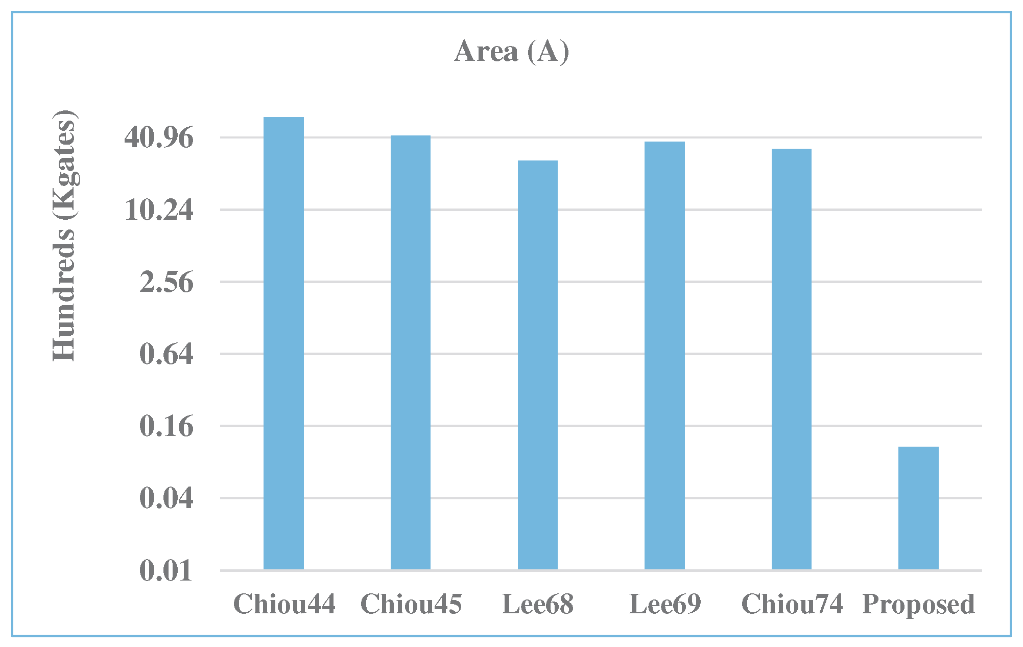
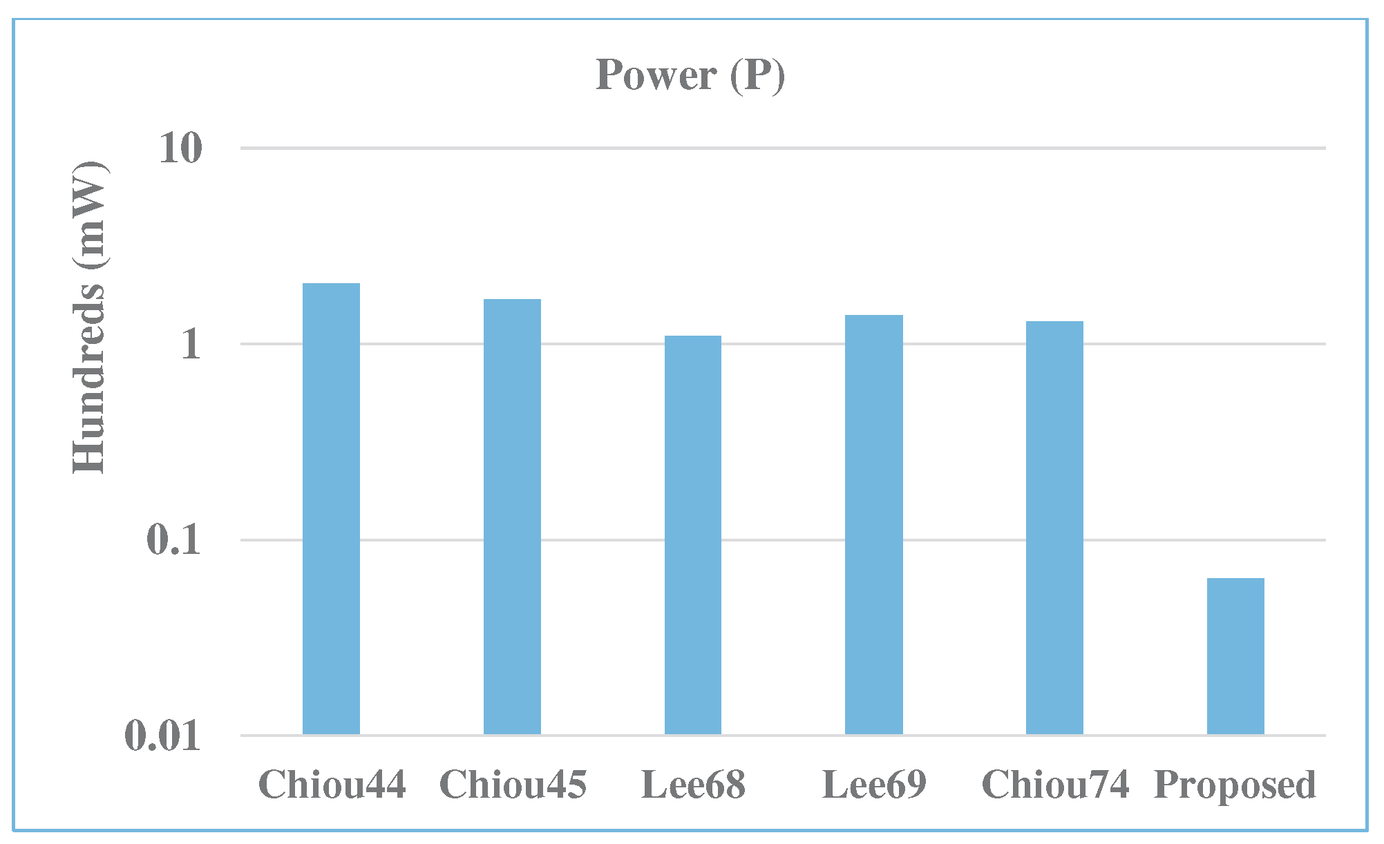
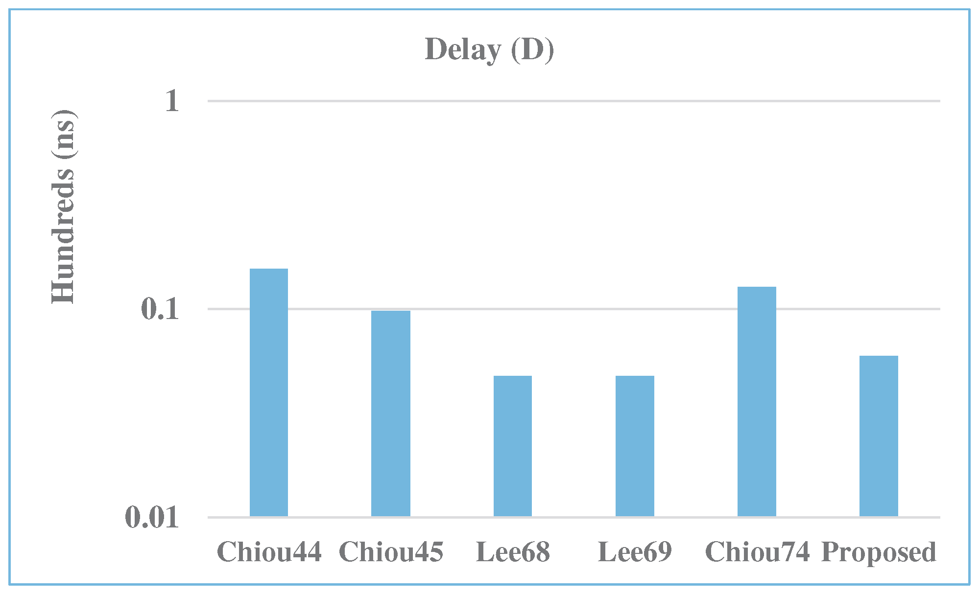
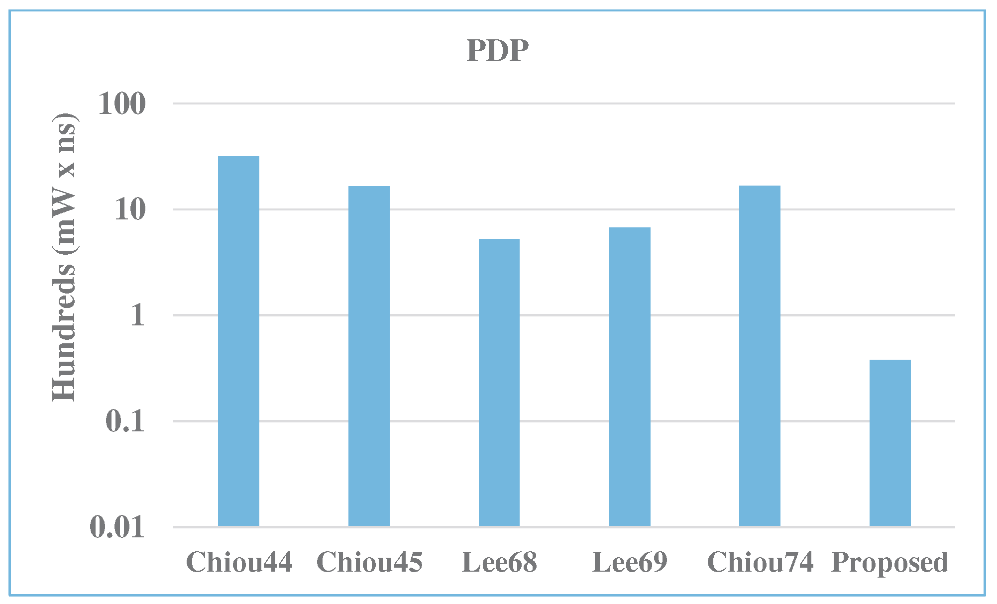
| Multiplier | m | A | D | P | ADP | PDP | A Saving | P Saving | ADP Saving | PDP Saving |
|---|---|---|---|---|---|---|---|---|---|---|
| [Kgates] | [ns] | [mW] | (%) | (%) | (%) | (%) | ||||
| Chiou [44] | 283 | 6082.6 | 15.6 | 202.3 | 95,117.0 | 3162.7 | 99.8 | 96.9 | 99.9 | 98.8 |
| Chiou [45] | 283 | 4276.3 | 9.8 | 169.7 | 41,720.3 | 1655.3 | 99.7 | 96.2 | 99.8 | 97.7 |
| Lee [68] | 283 | 2631.2 | 4.8 | 109.5 | 12,562.2 | 522.6 | 99.6 | 94.2 | 99.5 | 92.8 |
| Lee [69] | 283 | 3771.2 | 4.8 | 140.4 | 18,005.1 | 670.3 | 99.7 | 95.5 | 99.6 | 94.3 |
| Chiou [74] | 283 | 3273.6 | 12.8 | 130.6 | 41,904.4 | 1671.4 | 99.7 | 95.1 | 99.8 | 97.7 |
| Proposed | 283 | 10.7 | 5.9 | 6.4 | 63.8 | 37.9 | - | - | - | - |
Disclaimer/Publisher’s Note: The statements, opinions and data contained in all publications are solely those of the individual author(s) and contributor(s) and not of MDPI and/or the editor(s). MDPI and/or the editor(s) disclaim responsibility for any injury to people or property resulting from any ideas, methods, instructions or products referred to in the content. |
© 2025 by the authors. Licensee MDPI, Basel, Switzerland. This article is an open access article distributed under the terms and conditions of the Creative Commons Attribution (CC BY) license (https://creativecommons.org/licenses/by/4.0/).
Share and Cite
Ibrahim, A.; Gebali, F. Optimizing Security of Radio Frequency Identification Systems in Assistive Devices: A Novel Unidirectional Systolic Design for Dickson-Based Field Multiplier. Systems 2025, 13, 154. https://doi.org/10.3390/systems13030154
Ibrahim A, Gebali F. Optimizing Security of Radio Frequency Identification Systems in Assistive Devices: A Novel Unidirectional Systolic Design for Dickson-Based Field Multiplier. Systems. 2025; 13(3):154. https://doi.org/10.3390/systems13030154
Chicago/Turabian StyleIbrahim, Atef, and Fayez Gebali. 2025. "Optimizing Security of Radio Frequency Identification Systems in Assistive Devices: A Novel Unidirectional Systolic Design for Dickson-Based Field Multiplier" Systems 13, no. 3: 154. https://doi.org/10.3390/systems13030154
APA StyleIbrahim, A., & Gebali, F. (2025). Optimizing Security of Radio Frequency Identification Systems in Assistive Devices: A Novel Unidirectional Systolic Design for Dickson-Based Field Multiplier. Systems, 13(3), 154. https://doi.org/10.3390/systems13030154