Effect of Deposition Pressure on the Microstructure and Optical Band Gap of Molybdenum Disulfide Films Prepared by Magnetron Sputtering


Abstract
:1. Introduction
2. Experimental Details
2.1. Preparation of MoS2 Films
2.2. Characterization of MoS2 Films
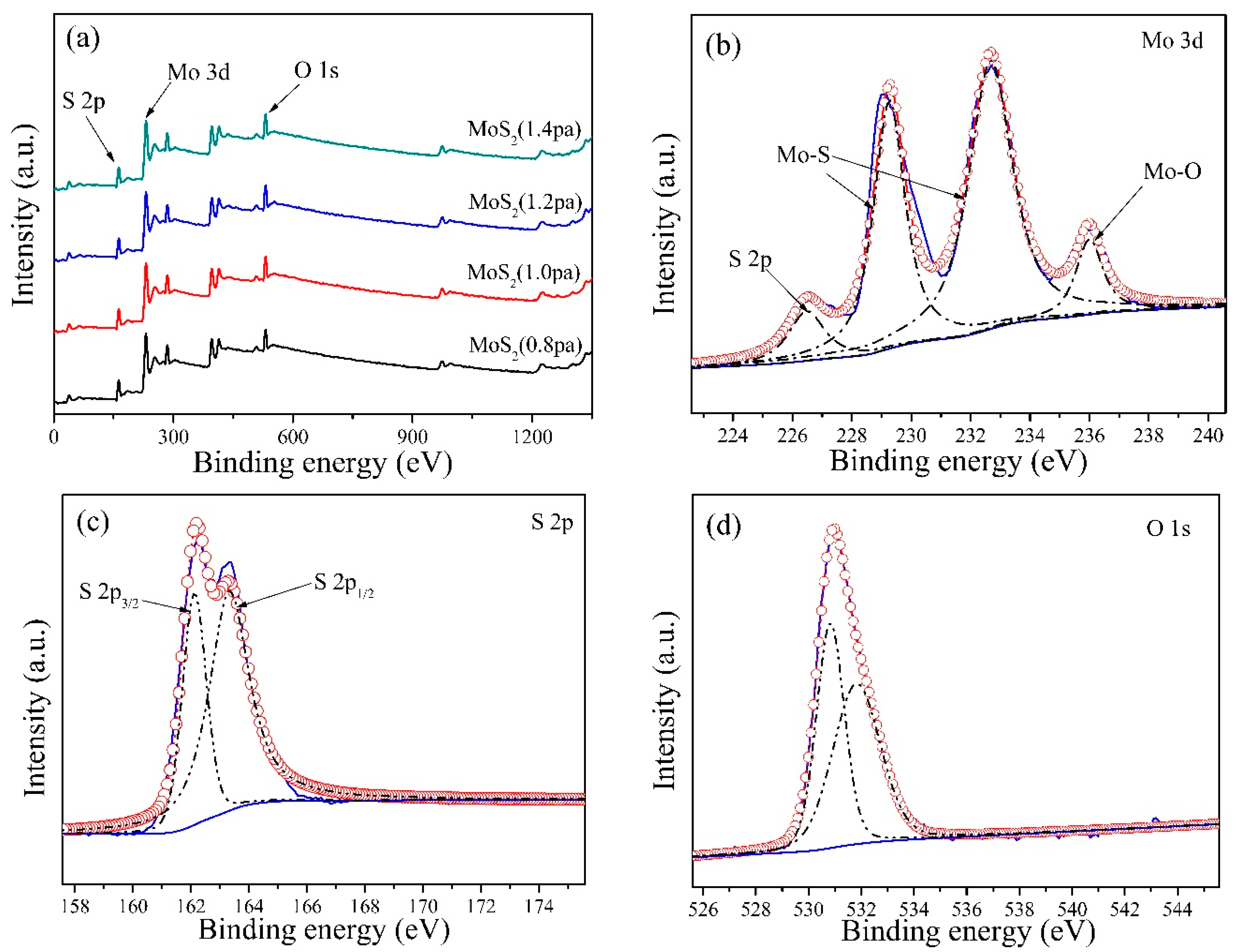
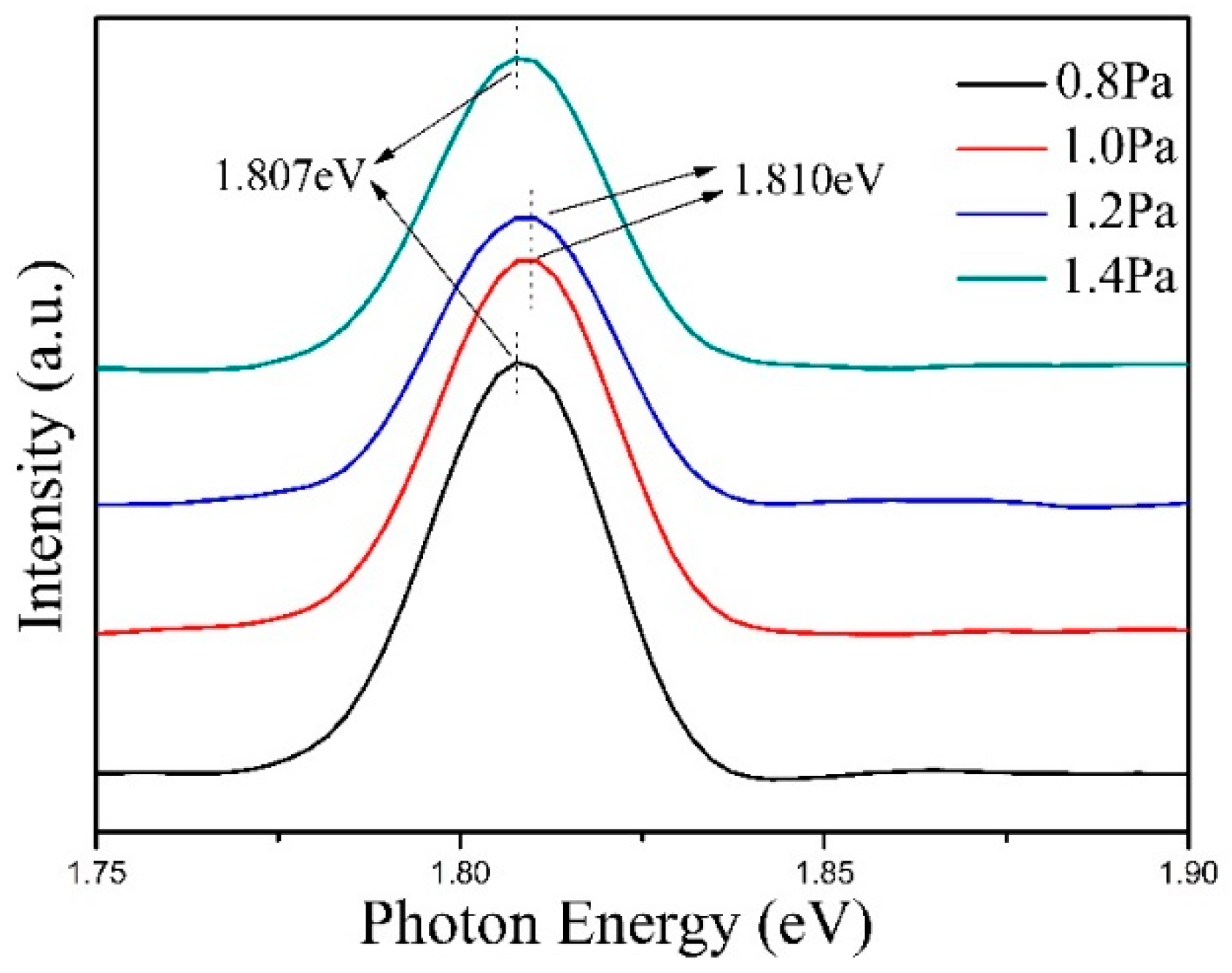
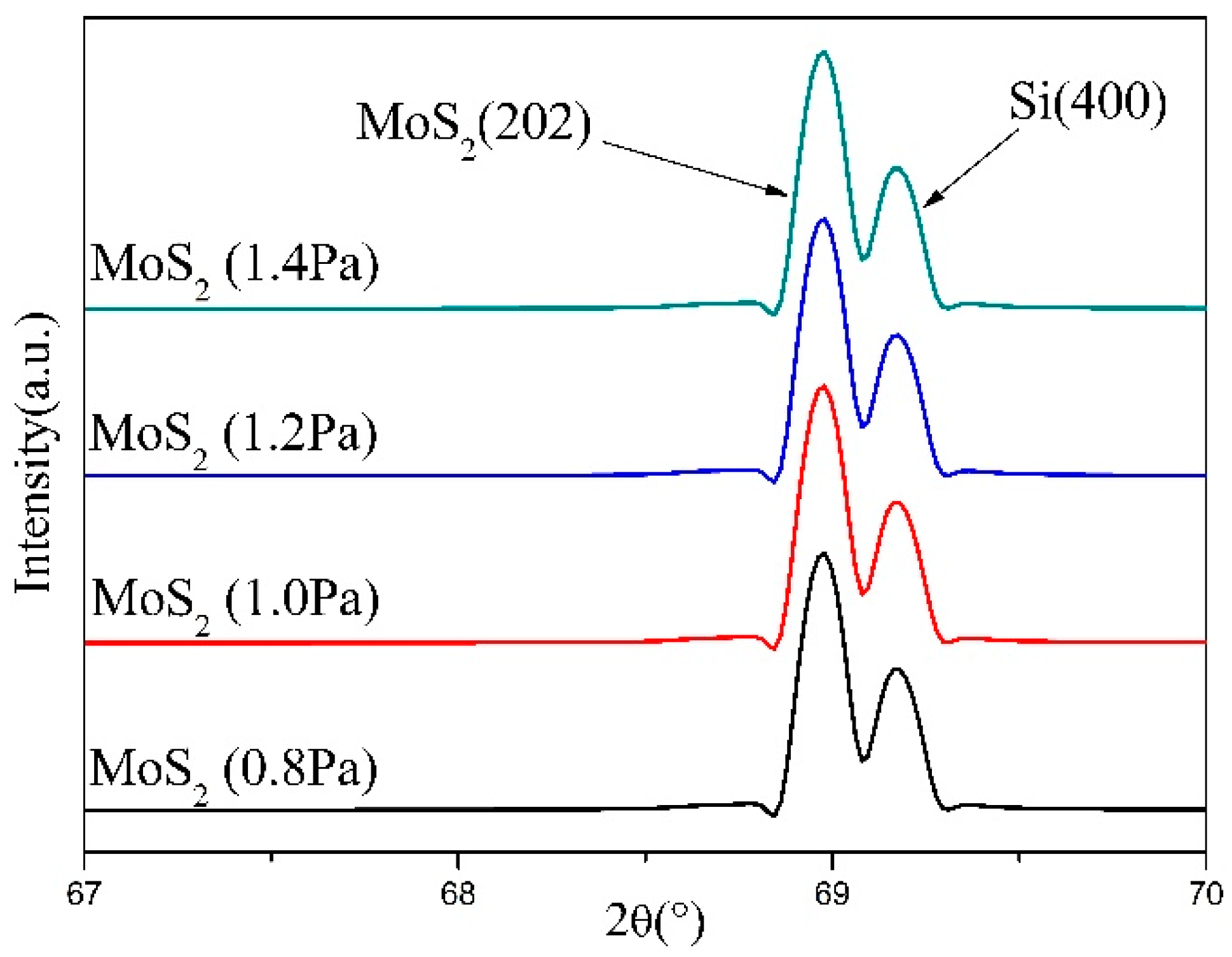
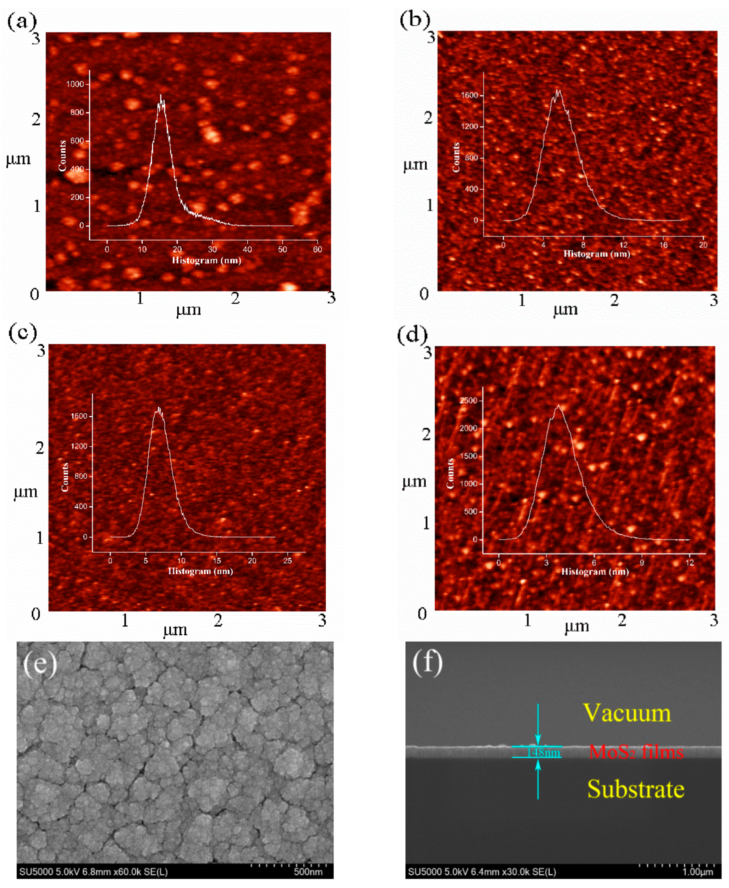
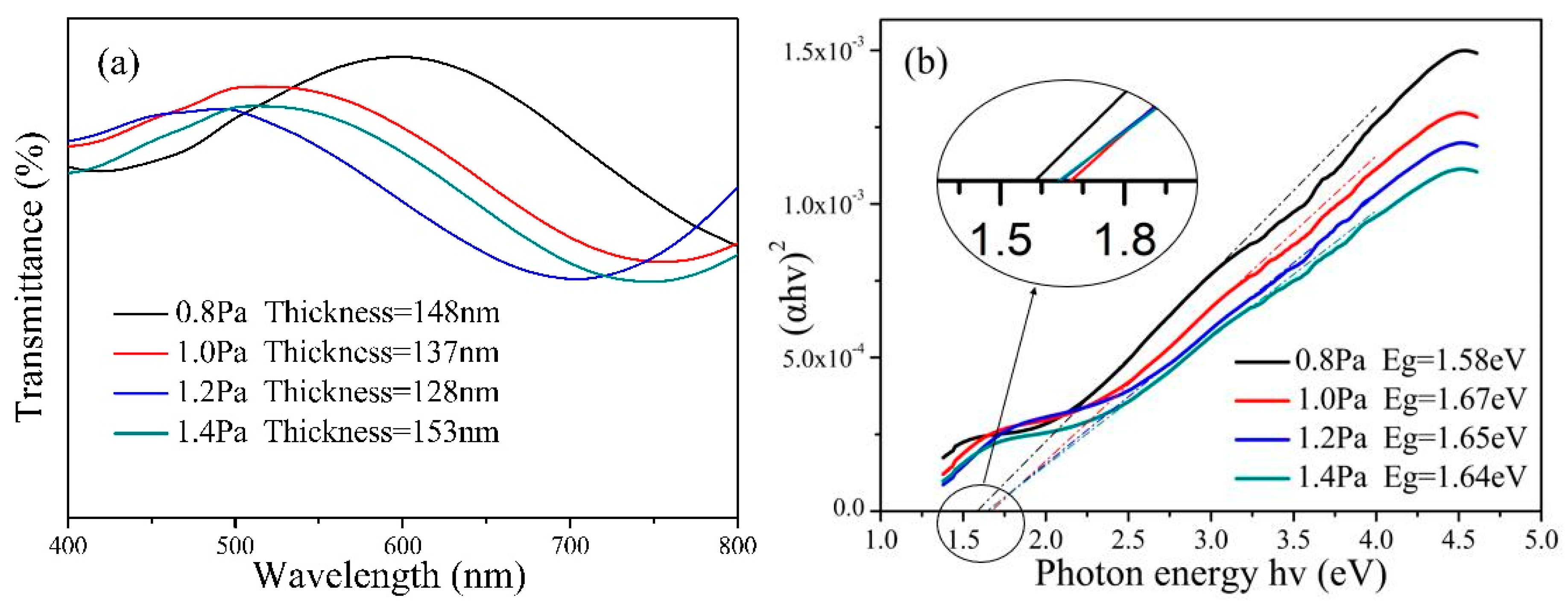
3. Results and Discussion
4. Conclusions
Author Contributions
Funding
Conflicts of Interest
References
- Shi, E.; Gao, Y.; Finkenauer, B.P.; Coffey, A.H.; Dou, L.T. Two-dimensional halide perovskite nanomaterials and heterostructures. Chem. Soc. Rev. 2018, 47, 6046–6072. [Google Scholar] [CrossRef] [PubMed]
- Wang, G.; Chernikov, A.; Glazov, M.M.; Heinz, T.F.; Marie, X.; Amand, T.; Urbaszek, B. Colloquium: Excitons in atomically thin transition metal dichalcogenides. Rev. Mod. Phys. 2018, 90, 021001. [Google Scholar] [CrossRef]
- Zhang, X.; Lai, Z.; Ma, Q.; Zhang, H. Novel structured transition metal dichalcogenide nanosheets. Chem. Soc. Rev. 2018, 47, 3301–3338. [Google Scholar] [CrossRef] [PubMed]
- Hu, Z.; Wu, Z.; Han, C.; He, J.; Ni, Z.H.; Chen, W. Two-dimensional transition metal dichalcogenides: Interface and defect engineering. Chem. Soc. Rev. 2018, 47, 3100–3128. [Google Scholar] [CrossRef] [PubMed]
- Govindasamy, M.; Chen, S.M.; Mani, V.; Devasenathipathy, R.; Umamaheswari, R.; Santhanaraj, K.J.; Sathiyan, A. Molybdenum disulfide nanosheets coated multiwalled carbon nanotubes composite for highly sensitive determination of chloramphenicol in food samples milk, honey and powdered milk. J. Colloid Interface Sci. 2017, 485, 129–136. [Google Scholar] [CrossRef] [PubMed]
- Zhang, H.; Zhou, W.; Liu, Q.; Yang, Z.X.; Pan, J.L.; Ouyang, F.P.; Xu, H. Transport properties and device-design of Z-shaped MoS2 nanoribbon planar junctions. Phys. E 2017, 92, 143–147. [Google Scholar] [CrossRef]
- Chen, Q.; Wang, W.; Peeters, F.M. Magneto-polarons in monolayer transition-metal dichalcogenides. J. Appl. Phys. 2018, 123, 214303. [Google Scholar] [CrossRef]
- Joshi, N.; Hayasaka, T.; Liu, Y.M.; Liu, H.L.; Oliveira, O.N.; Lin, L.W. A review on chemiresistive room temperature gas sensors based on metal oxide nanostructures, graphene and 2D transition metal dichalcogenides. Microchim. Acta 2018, 185, 16. [Google Scholar] [CrossRef]
- Shi, L.; Zhao, T.S. Recent advances in inorganic 2D materials and their applications in lithium and sodium batteries. J. Mater. Chem. 2017, 5, 3735–3758. [Google Scholar] [CrossRef]
- Qi, M.; Xiao, J.R.; Gong, C.Y. Thermal annealing effects on the electrophysical characteristics of sputtered MoS2 thin films by Hall effect measurements. Semicond. Sci. Technol. 2019, 34, 9. [Google Scholar] [CrossRef]
- Choi, J.; Mun, J.; Wang, M.C.; Ashraf, A.; Kang, S.W.; Nam, S. Hierarchical, dual-scale structures of atomically thin MoS2 for tunable wetting. Nano Lett. 2017, 17, 1756–1761. [Google Scholar] [CrossRef] [PubMed]
- Gunda, R.K.; Narala, S.K.R. Evaluation of friction and wear characteristics of electrostatic solid lubricant at different sliding conditions. Surf. Coat. Technol. 2017, 332, 341–350. [Google Scholar] [CrossRef]
- Chen, B.; Meng, Y.; Sha, J.; Zhong, C.; Hua, W.B.; Zhao, N.Q. Preparation of MoS2/TiO2 based nanocomposites for photocatalysis and rechargeable batteries: Progress, challenges, and perspective. Nanoscale 2017, 10, 34–68. [Google Scholar] [CrossRef]
- Song, X.; Liu, X.; Yu, D.; Huo, C.X.; Ji, J.P.; Li, X.M.; Zhang, S.L.; Zou, Y.S.; Zhu, G.Y.; Wang, Y.J.; et al. Boosting two-dimensional MoS2/CsPbBr3 photodetectors via enhanced light absorbance and interfacial carrier separation. ACS Appl. Mater. Interfaces. 2018, 10, 2801–2809. [Google Scholar] [CrossRef] [PubMed]
- Wu, K.; Chen, B.; Zhang, X.; Zhang, S.F.; Guo, C.S.; Li, C.; Xiao, P.S.; Wang, J.; Zhou, L.J.; Zou, W.W.; et al. High-performance mode-locked and Q-switched fiber lasers based on novel 2D materials of topological insulators, transition metal dichalcogenides and black phosphorus: Review and perspective. Opt. Commun. 2018, 406, 214–229. [Google Scholar] [CrossRef]
- Chen, Q.; Li, L.L.; Peeters, F.M. Magnetic field dependence of electronic properties of MoS2 quantum dots with different edges. Phys. Rev. 2018, 97, 085437. [Google Scholar] [CrossRef]
- Guo, J.; Jiang, J.; Yang, B. Low-voltage electric-double-layer MoS2 transistor gated via water solution. Solid-State Electron. 2018, 150, 8–15. [Google Scholar] [CrossRef]
- Guo, J.; Xie, D.; Yang, B.; Jiang, J. Low-Power logic computing realized in a single electric-double-layer MoS2 transistor gated with polymer electrolyte. Solid-State Electron. 2018, 144, 1–6. [Google Scholar] [CrossRef]
- Chen, Q.; Li, L.L.; Peeters, F.M. Inner and outer ring states of MoS2 quantum rings: Energy spectrum, charge and spin currents. J. Appl. Phys. 2019, 125, 244303. [Google Scholar] [CrossRef]
- Zhang, Y.; Zeng, W.; Li, Y. The hydrothermal synthesis of 3D hierarchical porous MoS2 microspheres assembled by nanosheets with excellent gas sensing properties. J. Alloy. Compd. 2018, 749, 355–362. [Google Scholar] [CrossRef]
- Windom, B.C.; Sawyer, W.G.; Hahn, D.W. A Raman spectroscopic study of MoS2 and MoO3: Applications to tribological systems. Tribol. Lett. 2011, 42, 301–310. [Google Scholar] [CrossRef]
- Shi, J.; Wu, D.; Zheng, X.; Xie, D.D.; Song, F.; Zhang, X.A.; Jiang, J.; Yuan, X.M.; Gao, Y.L.; Huang, H. From MoO2@MoS2 core-shell nanorods to MoS2 nanobelts. Phys. Status Solidi B 2018, 255, 1800254. [Google Scholar] [CrossRef]
- Liu, Y.; Peng, X.S. Recent advances of supercapacitors based on two-dimensional materials. Appl. Mater. Today 2017, 8, 104–115. [Google Scholar] [CrossRef]
- Mak, K.F.; Lee, C.; Hone, J.; Shan, J.; Heinz, T.F. Atomically thin MoS2: A new direct-gap semiconductor. Phys. Rev. Lett. 2010, 105, 136805. [Google Scholar] [CrossRef] [PubMed]
- Radisavljevic, B.; Radenovic, A.; Brivio, J.; Giacometti, V.; Kis, A. Single-layer MoS2 transistors. Nat. Nanotechnol. 2011, 6, 147–150. [Google Scholar] [CrossRef] [PubMed]
- Oyedele, A.D.; Yang, S.; Liang, L.; Puretzky, A.A.; Wang, K.; Zheng, J.J.; Yu, P.; Pudasaini, P.R.; Ghosh, A.W.; Liu, Z. PdSe2: Pentagonal two-dimensional layers with high air stability for electronics. J. Am. Chem. Soc. 2017, 139, 14090–14097. [Google Scholar] [CrossRef] [PubMed]
- Zou, H.; Zeng, Q.; Peng, M.; Zhou, W.Z.; Dai, X.Y.; Ouyang, F.P. Electronic structures and optical properties of P and Cl atoms adsorbed/substitutionally doped monolayer MoS2. Solid State Commun. 2018, 280, 6–12. [Google Scholar] [CrossRef]
- Late, D.J.; Huang, Y.K.; Liu, B.; Acharya, J.; Shirodkar, S.N.; Luo, J.J.; Yan, A.M.; Charles, D.; Waghmare, U.V.; Dravid, V.P.; et al. Sensing behavior of atomically thin-layered MoS2 transistors. ACS Nano 2013, 7, 4879–4891. [Google Scholar] [CrossRef] [PubMed]
- Ji, Q.; Zhang, Y.; Zhang, Y.; Liu, Z.F. Chemical vapour deposition of group-VIB metal dichalcogenide monolayers: Engineered substrates from amorphous to single crystalline. Chem. Soc. Rev. 2015, 44, 2587–2602. [Google Scholar] [CrossRef] [PubMed]
- Lv, R.; Robinson, J.A.; Schaak, R.E.; Sun, D.; Sun, Y.F.; Mallouk, T.E.; Terrones, M. Transition metal dichalcogenides and beyond: Synthesis, properties, and applications of single- and few-layer nanosheets. Acc. Chem. Res. 2015, 48, 56–64. [Google Scholar] [CrossRef]
- Splendiani, A.; Sun, L.; Zhang, Y.; Li, T.S.; Kim, J.; Chim, C.Y.; Galli, G.; Wang, F. Emerging photoluminescence in monolayer MoS2. Nano Lett. 2010, 10, 1271–1275. [Google Scholar] [CrossRef] [PubMed]
- Eda, G.; Yamaguchi, H.; Voiry, D.; Fujita, T.; Chen, M.W.; Chhowalla, M. Photoluminescence from chemically exfoliated MoS2. Nano Lett. 2011, 11, 5111–5116. [Google Scholar] [CrossRef] [PubMed]
- Cadiz, F.; Courtade, E.; Robert, C.; Wang, G.; Shen, Y.; Cai, H.; Taniguchi, T.; Watanabe, K.; Carrere, H.; Lagarde, D.; et al. Excitonic linewidth approaching the homogeneous limit in MoS2-based van der waals heterostructures. Phys. Rev. X 2017, 7, 021026. [Google Scholar] [CrossRef]
- Nan, H.; Wang, Z.; Wang, W.; Liang, Z.; Lu, Y.; Chen, Q.; He, D.W.; Tan, P.H.; Miao, F.; Wang, X.R.; et al. Strong photoluminescence enhancement of MoS2 through defect engineering and oxygen bonding. ACS Nano 2014, 8, 5738–5745. [Google Scholar] [CrossRef] [PubMed]
- Wang, S.; Wang, Z.; Qin, J.; Wang, W.D.; Li, W.Y.; He, D.W. Nanocrystalline MoS2 through directional growth along the (002) crystal plane under high pressure. Mater. Chem. Phys. 2011, 130, 170–174. [Google Scholar] [CrossRef]
- Bel Haj Mohamed, N.; Haouari, M.; Zaaboub, Z.; Hassen, F.; Maaref, H.; Ben Ouada, H. Effect of surface on the optical structure and thermal properties of organically capped CdS nanoparticles. J. Phys. Chem. Solids 2014, 75, 936–944. [Google Scholar] [CrossRef]
- Xiao, J.; Qi, M.; Gong, C.; Wang, Z.Y.; Jiang, A.H.; Ma, J.F.; Cheng, Y. Crystal structure and optical properties of silver-doped copper nitride films (Cu3N: Ag) prepared by magnetron sputtering. J. Phys. D 2018, 51, 055305. [Google Scholar] [CrossRef]
- Hassan, A.; Irfan, M.; Jiang, Y. Quantum confinement effect and size-dependent photoluminescence in laser ablated ultra-thin GZO films. Mater. Lett. 2018, 210, 358–362. [Google Scholar] [CrossRef]
- Li, X.; Wang, T.; Jiang, F.; Liu, J.; Liu, P.; Liu, G.Q.; Xu, J.K.; Liu, C.C.; Jiang, Q.L. Optimizing thermoelectric performance of MoS2 films by spontaneous noble metal nanoparticles decoration. J. Alloy. Compd. 2019, 781, 744–750. [Google Scholar] [CrossRef]
- Pradhan, G.; Sharma, A.K. Temperature controlled 1T/2H phase ratio modulation in mono- and a few layered MoS2 films. Appl. Surf. Sci. 2019, 479, 1236–1245. [Google Scholar] [CrossRef]
- Matsuura, K.; Ohashi, T.; Muneta, I.; Ishihara, S.; Kakushima, K.; Tsutsui, K.; Ogura, A.; Wakabayashi, H. Low-carrier-density sputtered MoS2 film by vapor-phase sulfurization. J. Electron. Mater. 2018, 47, 3497–3501. [Google Scholar] [CrossRef]
- Zhuang, W.; Li, H.; Li, W.; Fan, X.Q.; He, J.F.; Cai, Z.B.; Fu, W.; Zhang, G.G.; Wan, S.H.; Zhu, M.H. Probing fretting performance of DLC and MoS2 films under fluid lubrication. Appl. Surf. Sci. 2019, 478, 661–679. [Google Scholar] [CrossRef]
- Amin, R.; Hossain, M.A.; Zakaria, Y. Interfacial kinetics and ionic diffusivity of the electrodeposited MoS2 film. Acs Appl. Mater. Interfaces 2018, 10, 13509–13518. [Google Scholar] [CrossRef] [PubMed]
- Sarma, S.; Ray, S.C. Trigonal (1T) and hexagonal (2H) mixed phases MoS2 thin films. Appl. Surf. Sci. 2019, 474, 227–231. [Google Scholar] [CrossRef]
- Kim, H.; Park, T.; Park, S.; Leem, M.; Ahn, W.; Lee, H.; Lee, C.; Lee, E.; Jeong, S.J.; Park, S.; et al. Ultrathin monolithic HfO2 formed by Hf-seeded atomic layer deposition on MoS2: Film characteristics and its transistor application. Thin Solid Film. 2019, 673, 112–118. [Google Scholar] [CrossRef]
- Jiang, Q.; Sun, L.; Bi, J.; Liang, S.J.; Li, L.Y.; Yu, Y.; Wu, L. MoS2 quantum dots-modified covalent triazine-based frameworks for enhanced photocatalytic hydrogen evolution. ChemSusChem. 2018, 11, 1108–1113. [Google Scholar] [CrossRef]
- Wang, W.; Chen, X.; Zeng, X.; Wu, S.X.; Zeng, Y.; Hu, Y.S.; Xu, S.; Zhou, G.T.; Cui, H.X. Investigation of the growth process of continuous monolayer MoS2 films prepared by chemical vapor deposition. J. Electron. Mater. 2018, 47, 5509–5517. [Google Scholar] [CrossRef]
- Kathiravan, D.; Huang, B.R.; Saravanan, A.; Prasannan, A.; Hong, P.D. Highly enhanced hydrogen sensing properties of sericin-induced exfoliated MoS2 nanosheets at room temperature. Sens. Actuators B 2019, 279, 138–147. [Google Scholar] [CrossRef]
- Chen, F.; Wang, T.; Wang, L.; Su, W.T. Two-step fabrication of large-scale MoS2 hollow flakes. CrystEngComm 2018, 20, 5619–5624. [Google Scholar] [CrossRef]


| Crystal Parameter | Pressure | |||
|---|---|---|---|---|
| 0.8 Pa | 1.0 Pa | 1.2 Pa | 1.4 Pa | |
| a (nm) | 3.851 | 3.828 | 3.829 | 3.828 |
| d (nm) | 1.362 | 1.354 | 1.354 | 1.353 |
| D (nm) | 22.804 | 30.353 | 28.782 | 31.499 |
| Sample Parameter | Pressure | |||
|---|---|---|---|---|
| 0.8 Pa | 1.0 Pa | 1.2 Pa | 1.4 Pa | |
| Roughness (nm) | 16.83 | 5.96 | 7.21 | 4.08 |
| Thickness (nm) | 148 | 137 | 128 | 153 |
© 2019 by the authors. Licensee MDPI, Basel, Switzerland. This article is an open access article distributed under the terms and conditions of the Creative Commons Attribution (CC BY) license (http://creativecommons.org/licenses/by/4.0/).
Share and Cite
Gong, C.; Xiao, J.; Zhu, L.; Wang, Z.; Ma, S. Effect of Deposition Pressure on the Microstructure and Optical Band Gap of Molybdenum Disulfide Films Prepared by Magnetron Sputtering. Coatings 2019, 9, 570. https://doi.org/10.3390/coatings9090570
Gong C, Xiao J, Zhu L, Wang Z, Ma S. Effect of Deposition Pressure on the Microstructure and Optical Band Gap of Molybdenum Disulfide Films Prepared by Magnetron Sputtering. Coatings. 2019; 9(9):570. https://doi.org/10.3390/coatings9090570
Chicago/Turabian StyleGong, Chenyang, Jianrong Xiao, Liwen Zhu, Zhiyong Wang, and Songshan Ma. 2019. "Effect of Deposition Pressure on the Microstructure and Optical Band Gap of Molybdenum Disulfide Films Prepared by Magnetron Sputtering" Coatings 9, no. 9: 570. https://doi.org/10.3390/coatings9090570
APA StyleGong, C., Xiao, J., Zhu, L., Wang, Z., & Ma, S. (2019). Effect of Deposition Pressure on the Microstructure and Optical Band Gap of Molybdenum Disulfide Films Prepared by Magnetron Sputtering. Coatings, 9(9), 570. https://doi.org/10.3390/coatings9090570