Design and Fabrication of a Narrow Bandpass Filter with Low Dependence on Angle of Incidence


Abstract
1. Introduction
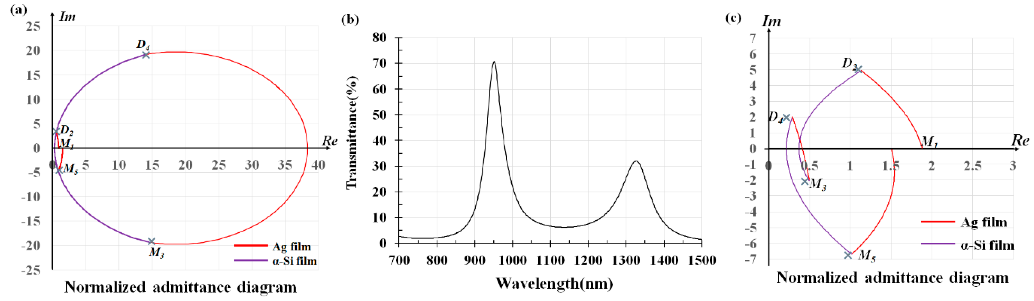
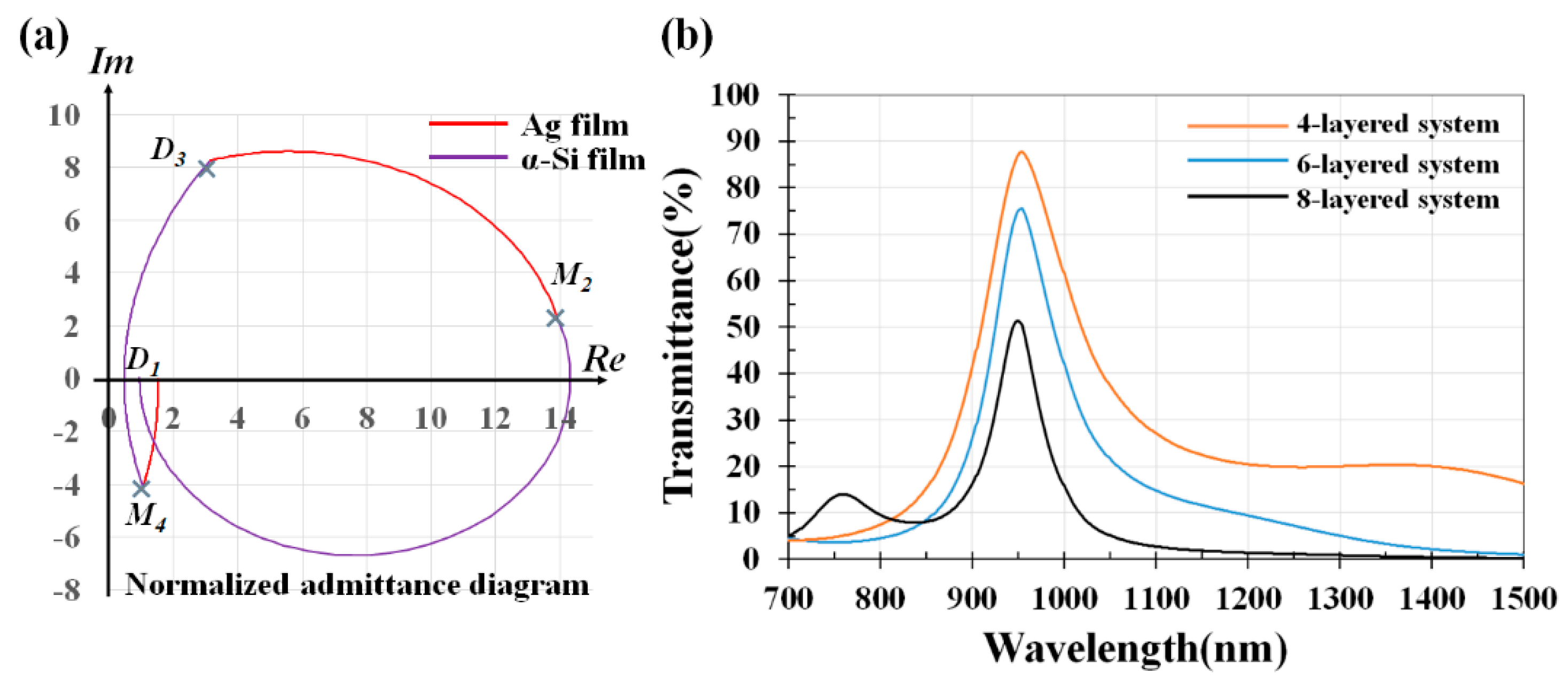
2. Methods
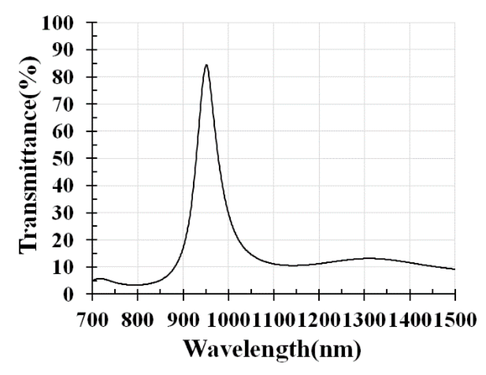
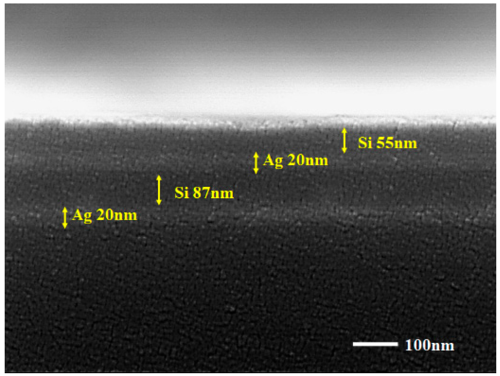
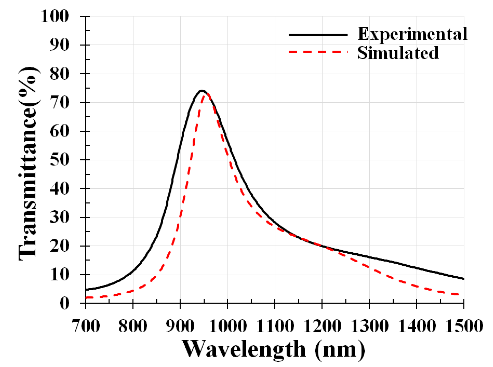
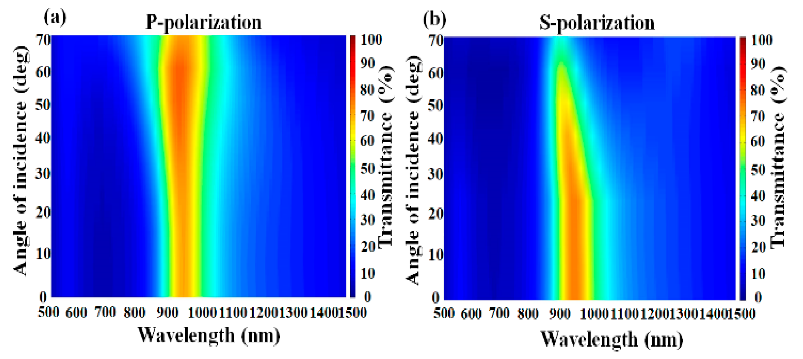
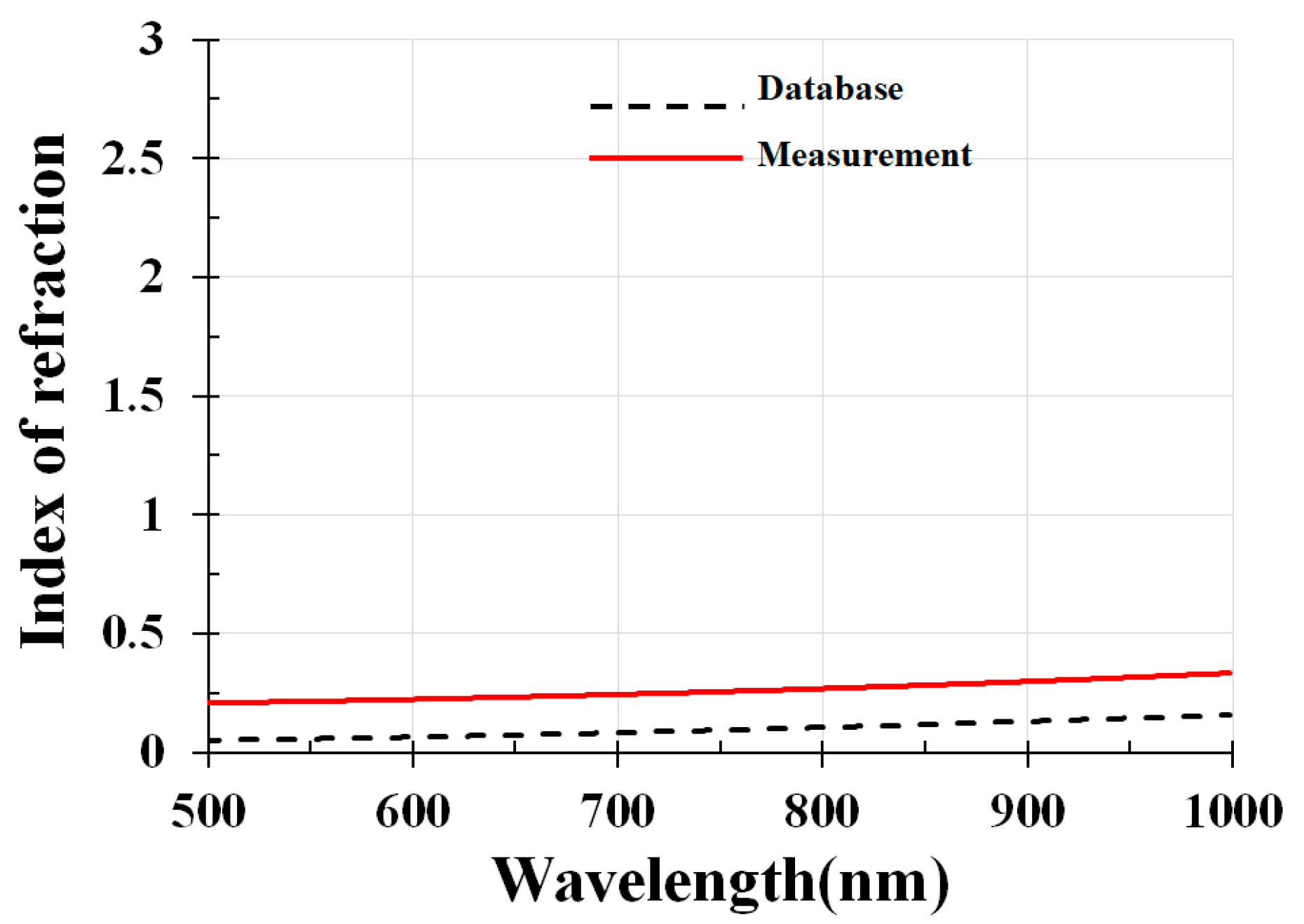
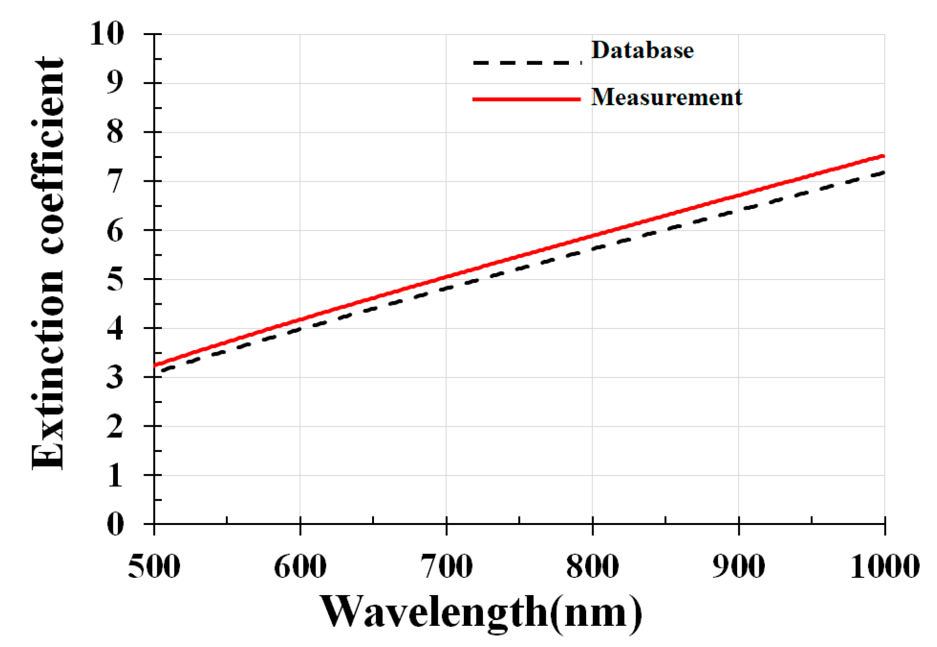
3. Experiments and Results
4. Conclusions
Author Contributions
Funding
Acknowledgments
Conflicts of Interest
Appendix A


References
- Koo, H.; Chen, M.; Pan, P. LCD-based color filter films fabricated by a pigment-based colorant photo resist inks and printing technology. Thin Solid Films 2006, 515, 896–901. [Google Scholar] [CrossRef]
- Ko, F.-J.; Shieh, H.-P.D. High-efficiency micro-optical color filter for liquid-crystal projection system applications. Appl. Opt. 2000, 39, 1159–1163. [Google Scholar] [CrossRef] [PubMed]
- Chung, D.; Shin, C.; Song, B.; Jung, M.; Yun, Y.; Nam, S.H.; Noh, C.; Kim, J.; Lee, S. Color filters for reflective display with wide viewing angle and high reflectivity based on metal dielectric multilayer. Appl. Phys. Lett. 2012, 101, 221120. [Google Scholar] [CrossRef]
- Kanamori, Y.; Shimono, M.; Hane, K. Fabrication of transmission color filters using silicon subwavelength gratings on quartz substrates. IEEE Photonics Technol. Lett. 2006, 18, 2126–2128. [Google Scholar] [CrossRef]
- Park, J.-G.; Kim, S.-H.; Magkiriadou, S.; Choi, T.M.; Kim, Y.-S.; Manoharan, V.N. Full-spectrum photonic pigments with non-iridescent structural colors through colloidal assembly. Angew. Chem. Int. Ed. 2014, 53, 2899–2903. [Google Scholar] [CrossRef] [PubMed]
- Macleod, H. Thin Film Optical Filters, 3rd ed.; Institute of Physics Publishing: Bristol, UK, 2001. [Google Scholar]
- Yang, C.; Shen, W.; Zhang, Y.; Li, K.; Fang, X.; Zhang, X.; Liu, X. Compact multilayer film structure for angle insensitive color filtering. Sci. Rep. 2015, 5, 9285. [Google Scholar] [CrossRef] [PubMed]
- Si, G.; Zhao, Y.; Lv, J.; Lu, M.; Wang, F.; Liu, H.; Xiang, N.; Huang, T.J.; Danner, A.J.; Teng, J.; et al. Reflective plasmonic color filters based on lithographically patterned silver nanorod arrays. Nanoscale 2013, 5, 6243–6248. [Google Scholar] [CrossRef] [PubMed]
- Ai, B.; Yu, Y.; Mohwald, H.; Zhang, G. Color displays: Responsive monochromatic color display based on nanovolcano arrays. Adv. Opt. Mater. 2013, 1, 724–731. [Google Scholar] [CrossRef]
- Lin, L.; Roberts, A. Angle-robust resonances in crossshaped aperture arrays. Appl. Phys. Lett. 2010, 97, 061109. [Google Scholar] [CrossRef]
- Xu, T.; Wu, Y.-K.; Luo, X.; Guo, L.J. Plasmonic nanoresonators for high-resolution colour filtering and spectral imaging. Nat. Commun. 2010, 59. [Google Scholar] [CrossRef] [PubMed]
- Jen, Y.-J.; Lee, C.-C.; Lu, K.-H.; Jheng, C.-Y.; Chen, Y.-J. Fabry-Perot based metal-dielectric multilayered filters and metamaterials. Opt. Exp. 2015, 23, 33008–33017. [Google Scholar] [CrossRef] [PubMed]
- Morita, M.; Ohmi, T.; Hasegawa, E.; Kawakami, M.; Ohwada, M. Growth of native oxide on a silicon surface. J. Appl. Phys. 1990, 68, 1272–1281. [Google Scholar] [CrossRef]
- Ryckman, J.D.; Reed, R.A.; Weller, R.A.; Fleetwood, D.M.; Weissa, S.M. Enhanced room temperature oxidation in silicon and porous silicon under 10 keV X-ray irradiation. J. Appl. Phys. 2010, 108, 113528. [Google Scholar] [CrossRef]


© 2018 by the authors. Licensee MDPI, Basel, Switzerland. This article is an open access article distributed under the terms and conditions of the Creative Commons Attribution (CC BY) license (http://creativecommons.org/licenses/by/4.0/).
Share and Cite
Jen, Y.-J.; Lin, M.-J. Design and Fabrication of a Narrow Bandpass Filter with Low Dependence on Angle of Incidence. Coatings 2018, 8, 231. https://doi.org/10.3390/coatings8070231
Jen Y-J, Lin M-J. Design and Fabrication of a Narrow Bandpass Filter with Low Dependence on Angle of Incidence. Coatings. 2018; 8(7):231. https://doi.org/10.3390/coatings8070231
Chicago/Turabian StyleJen, Yi-Jun, and Meng-Jie Lin. 2018. "Design and Fabrication of a Narrow Bandpass Filter with Low Dependence on Angle of Incidence" Coatings 8, no. 7: 231. https://doi.org/10.3390/coatings8070231
APA StyleJen, Y.-J., & Lin, M.-J. (2018). Design and Fabrication of a Narrow Bandpass Filter with Low Dependence on Angle of Incidence. Coatings, 8(7), 231. https://doi.org/10.3390/coatings8070231