Article

Preparation and Photoluminescence of Tungsten Disulfide Monolayer

College of Materials & Environmental Engineering, Hangzhou Dianzi University, Hangzhou 310018, China
*
Authors to whom correspondence should be addressed.
Coatings 2018, 8(6), 205; https://doi.org/10.3390/coatings8060205
Submission received: 20 April 2018 / Revised: 16 May 2018 / Accepted: 24 May 2018 / Published: 30 May 2018

Abstract

:
Tungsten disulfide (WS2) monolayer is a direct band gap semiconductor. The growth of WS2 monolayer hinders the progress of its investigation. In this paper, we prepared the WS2 monolayer through chemical vapor transport deposition. This method makes it easier for the growth of WS2 monolayer through the heterogeneous nucleation-and-growth process. The crystal defects introduced by the heterogeneous nucleation could promote the photoluminescence (PL) emission. We observed the strong photoluminescence emission in the WS2 monolayer, as well as thermal quenching, and the PL energy redshift as the temperature increases. We attribute the thermal quenching to the energy or charge transfer of the excitons. The redshift is related to the dipole moment of WS2.

1. Introduction

Tungsten disulfide (WS2) monolayer, a direct band gap semiconductor, shows strong photoluminescence (PL) emission [1,2]. The PL properties have attracted plenty of research interest.
Yun et al. [3] found the non-uniformity of the PL emission in WS2 monolayer. The exciton and charge carriers form the exciton complexes. Kim et al. [4] suspected that the PL emission originated from the exciton complexes. The inhomogeneous distribution of the charge carriers resulted in the PL emission non-uniformity. The PL emission energy shifts as the excitation power or sample temperature changes. For example, Gordo et al. found the laser irradiation changes the PL emission by introducing the carrier doping [5]. Rosenberger et al. studied the relationship between the PL intensity and defect density using conductive atomic force microscopy. They found the PL intensity increases with the decrease of the defect density. Furthermore, they proposed that the defects act as the nonradioactive recombination center [6]. The mechanism for PL emission is under exploration. Besides the charge carrier and defects, chemical doping and surface absorption have an effect on the PL emission. Yao et al. and Feng et al. found the PL energy changed as the WS2 monolayer was immersed into sodium sulfide (Na2S) solution, or coated with DNA nucleobases [7,8].
Before having full understanding of the PL emission mechanism, successful preparation of WS2 monolayer is challenging. Under this background, various methods have been applied for the preparation of WS2 monolayer/layers, such as exfoliation, atomic layer deposition, and pulsed laser deposition [9,10,11]. Since chemical vapor deposition (CVD) has been successfully applied to the deposition of large-scale two-dimensional materials, such as graphene and hexagonal boron nitride, the CVD method is carried forward for the synthesis of the WS2 monolayer [12,13,14]. Among various CVD methods, the sulfurization of tungsten oxide in sulfur vapor is a commonly used CVD method. Gutiérrez et al. deposited a thin film of tungsten oxide on the SiO2/Si substrate, then heated at 800 °C under argon and sulfur vapor. The lateral size of the WS2 monolayer with triangular shape is ~15 μm. The WS2 showed extraordinary photoluminescence emission at room temperature [2]. Cong et al. reported the growth of WS2 monolayer on the SiO2/Si substrate through sulfurization of tungsten oxide powders. The lateral size of triangular WS2 domain was up to hundreds of micrometers [15]. Before long, Gao et al. [16] reported the growth of WS2 monolayer with millimeter scale using catalyst. They found the photoluminescence (PL) emission intensity at 612.6 nm was 103 times stronger than bulk material. Cong et al. [15] and Gao et al. [16] found the PL emission was far stronger in the edge region, which is opposite to that of Gutiérrez’s observation. Besides the metal catalyst, WS2 monolayer growth is also sensitive to the promoter and surface condition. Li et al. found the addition of the alkali metal halides reduces the growth temperature (700–850 °C) [17]. In conclusion, the growth of WS2 monolayer is sensitive to the growth process. Much research into the preparation and photoluminescence needs to be done.
We recently reported the chemical vapor transport deposition of molybdenum disulfide monolayer [18]. Molybdenum disulfide reacted with the transport agent water vapor to form molybdenum oxide at high temperature. Then, the molybdenum oxide reacted with sulfur and transformed into a molybdenum disulfide monolayer at a low temperature. In this method, water vapor was used as the transport agent and the nucleation promoter. The introduction of water vapor promoted the molybdenum disulfide monolayer growth. WS2 and molybdenum disulfide are both transition metal dichalcogenides. An interesting question is whether this method can prepare WS2 monolayer. Here, we show that water vapor can promote the WS2 monolayer growth. The synthesized WS2 monolayer shows strong PL emission, and the PL is also sensitive to the temperature. Our findings, therefore, offer important clues to the transition metal dichalcogenides monolayer growth. The PL change couldalso be used as a detector of temperature change.

2. Materials and Methods

WS2 Layer Synthesis

WS2 monolayer was prepared by a previously reported chemical vapor transport deposition method, which was used for the growth of molybdenum disulfide monolayer on a silicon substrate with a 300 nm layer of oxide (SiO2/Si) [18]. WS2 powders (99.5% purity, Aladdin, Shanghai, China) were used as the precursor. The precursor (0.5 g) was loaded in the center of a one-inch-diameter tube furnace (Hefei Kejing Materials technology Co., Ltd., Hefei, China), and heated to 1000 °C from room temperature in 30 min. The substrate was put downstream of the tube furnace. During the above process, the substrate was heated to 710–850 °C and kept at 710–850 °C for 60 min, before the furnace was turned off and cooled naturally to room temperature. The water vapor was carried into the tube by Ar/H2 (75 Torr, Ar/H2 70 sccm) during the whole heating stage.
Optical microscope image was carried out on a Jiangnan MV3000 digital microscope (Nanjing Jiangnan Novel Optics Co., Ltd., Nanjing, China). Tapping mode atomic force microscopy (AFM) was conducted with an Agilent 5500 (Agilent Technologies, Palo Alto, CA, USA) in the air. Raman spectra and photoluminescence (PL) were measured on a home-built micro-Raman setup that consists of a 532 nm solid state laser, a Nikon inverted microscope (Ti eclipse, Nikon, Tokyo, Japan), a long pass edge filter (Semrock, Rochester, NY, USA), and a Raman spectrometer (iHR320, Horiba, Kyoto, Japan) with an attached thermoelectric-cooled CCD camera (Andor Syncerity, Horiba) at room temperature. PL mapping was measured on a Nib400 fluorescence microscope (Nanjing Jiangnan Novel Optics Co., Ltd., Nanjing, China). X-ray diffraction (XRD) was performed on a Thermo ARLXTRA (Thermo Electron, Waltham, MA, USA).

3. Results and Discussion

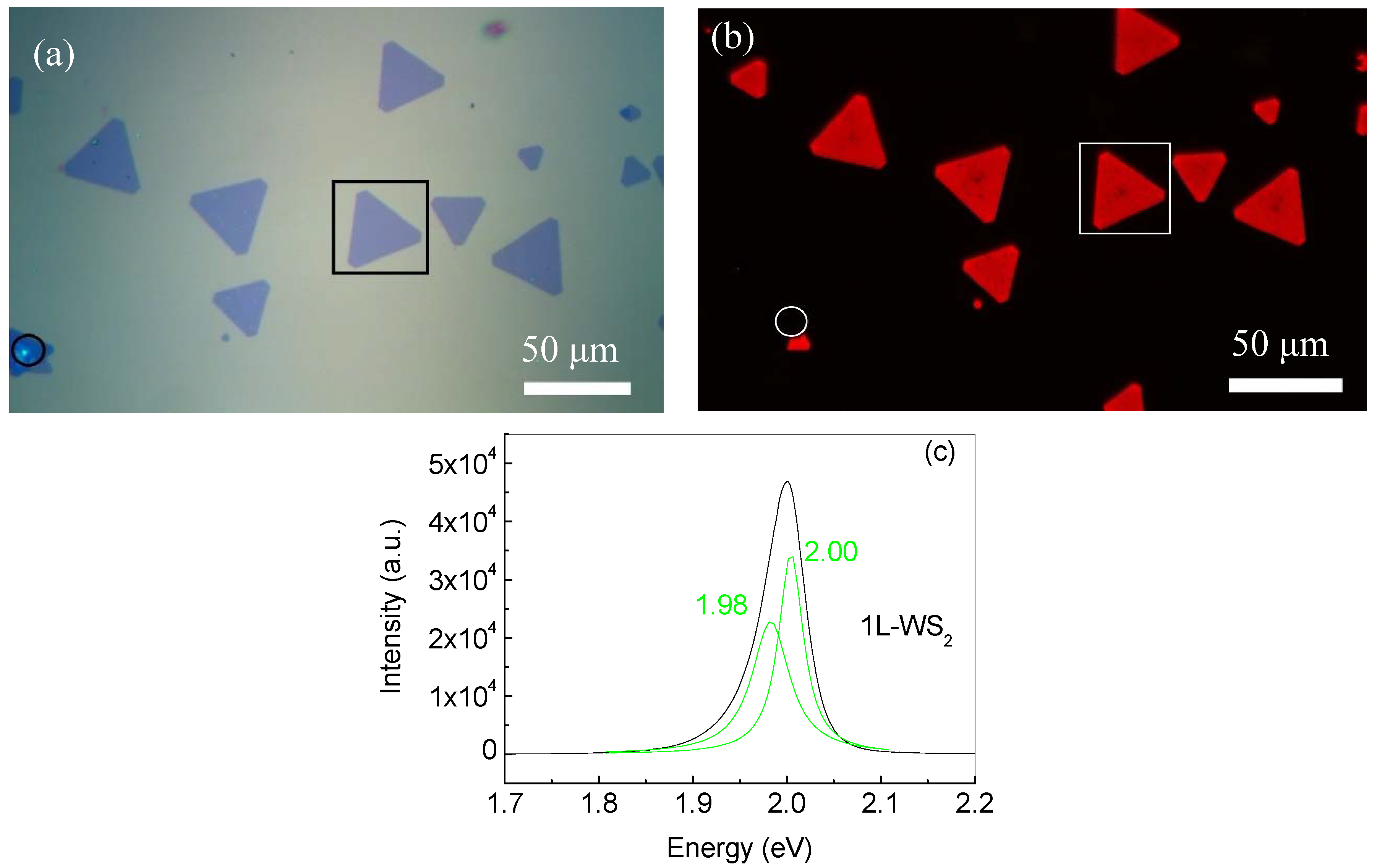
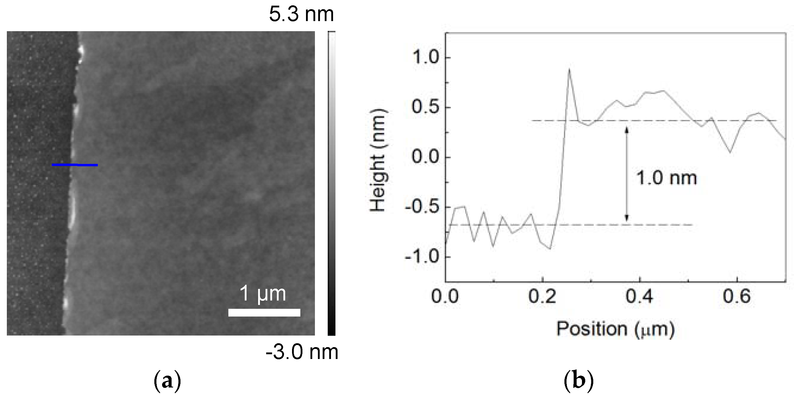
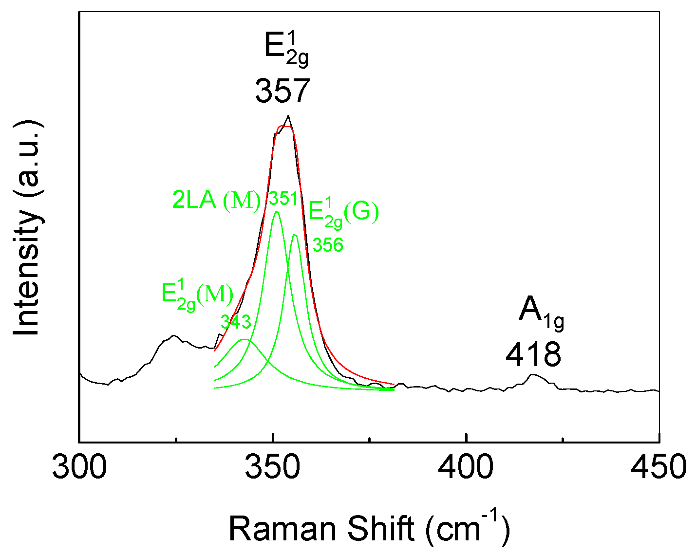
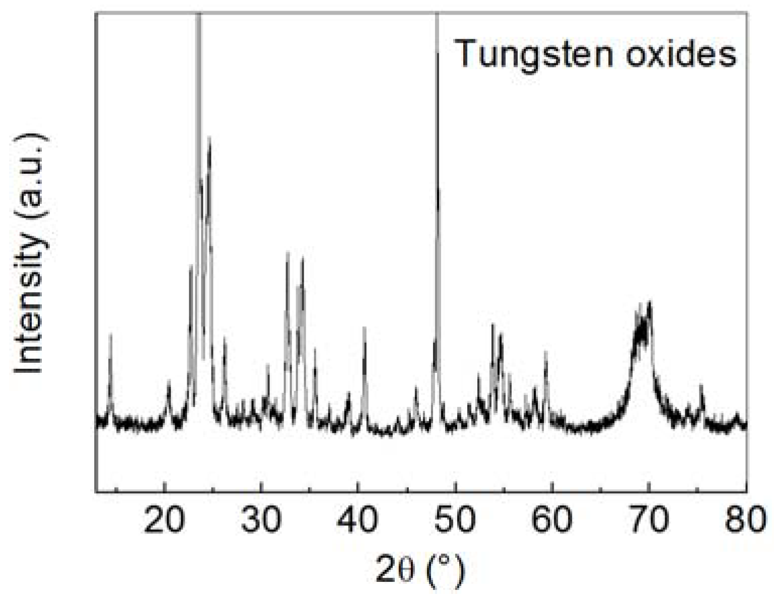
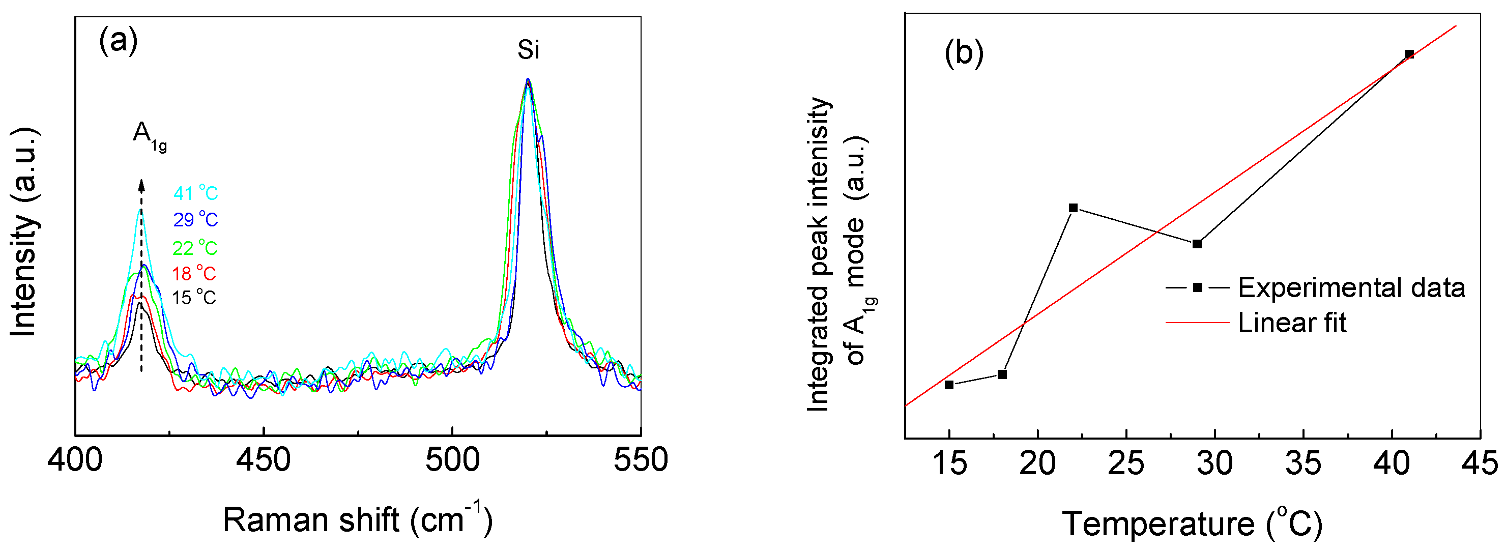
3.1. WS2 Monolayer Growth

Figure 1a shows the optical image of the separated triangular WS2 monolayer grown on the SiO2/Si substrate in the presence of H2O vapor. Except for the black circled area which is WS2 multilayers, other areas with a triangular shape are the WS2 monolayer. The uniform color contrast indicates that the thickness of the WS2 monolayer is uniform. The lateral size of the monolayer is up to ca. 38 μm.
Figure 1b shows the PL mapping of the WS2 monolayer using an excitation wavelength of 485 nm. PL mapping was measured at the same location as the one in Figure 1a (marked with black square). We found the WS2 monolayer emitted strong PL while the WS2 multilayer (circled area) gave out no PL emission. Intensive PL emission is due to the direct band gap structure of monolayer. The valence band maximum and the conduction band minimum in the bulk WS2 occur at different k (wave vector) values in the Brillouin zone. While in the monolayer, the valence band maximum and the conduction band minimum occur at the same position (K point). Therefore, the indirect-to-direct band gap conversion occurs as the thickness of the WS2 is reduced to a monolayer [19]. The direct band gap is ca. 2.05 eV [20].
Figure 1c shows the PL spectrum of the WS2 monolayer excited by a 532 nm laser. The peak energy (~2.0 eV) is lower than the band gap, and is considered to be related to the excitons [4]. In this paper, the WS2 was synthesized by heterogeneous nucleation-and-growth process (discussed in the section of the mechanism below). The heterogeneous nucleation could promote the crystal growth as well as the introduction of crystal defects. The crystal defects play a significant role in the PL emission. Lattice defects act as nonradiative recombination centers in general semiconductor.
However, recent investigations revealed that the lattice defects can promote the PL emission by forming charged exciton and defect-bound excitons with neutral excitons [4,21]. We fit the strong PL peak at ca. 2.0 eV with Lorentzian lineshape functions, as shown in Figure 1c. The two components at 2.00 eV and 1.98 eV are possibly due to the transition of charged excitons and defect-bound excitons, respectively. The intensive PL and single emission peak are characteristics for WS2 monolayer, and once again, testify that the thickness of the WS2 is monolayer [2,16].
Figure 2a shows the AFM image of the WS2 flake edge within the square in Figure 1a. The height of the edge is 1.0 ± 0.1 nm, which is larger than the theoretical value (0.6 nm) of the monolayer thickness [22]. Considering the tip–substrate interaction and the surface adsorbate, the flake should be a monolayer [18].
Figure 3 shows the Raman spectrum of the WS2 monolayer. The anti-symmetric peak E12g at ca. 357 cm−1 can be fitted with Lorentzian function whose three subpeaks are at 343, 351, and 356 cm−1, corresponding to the in-plane vibrational E12g(M) mode, the longitudinal acoustic phonon 2LA(M) mode, and the in-plane vibrational E12g(Γ), respectively. The peak at 418 cm−1 (A1g) is assigned to the out-of-plane vibrational mode of two sulfur atoms [4,20].
To study the growth mechanism of the WS2 monolayer, we analyzed the residue of the precursor by X-ray diffraction (XRD). Figure 4 shows the X-ray diffraction (XRD) of the precursor after heating in water vapor for more than 20 h at 1000 °C. Peaks of tungsten oxides are found in the XRD spectrum. Therefore, the WS2 reacted with water vapor to form tungsten oxides, which further sulfurized and transformed into the WS2 monolayer. Tungsten oxides acted as the heterogeneous nucleation during the growth process.

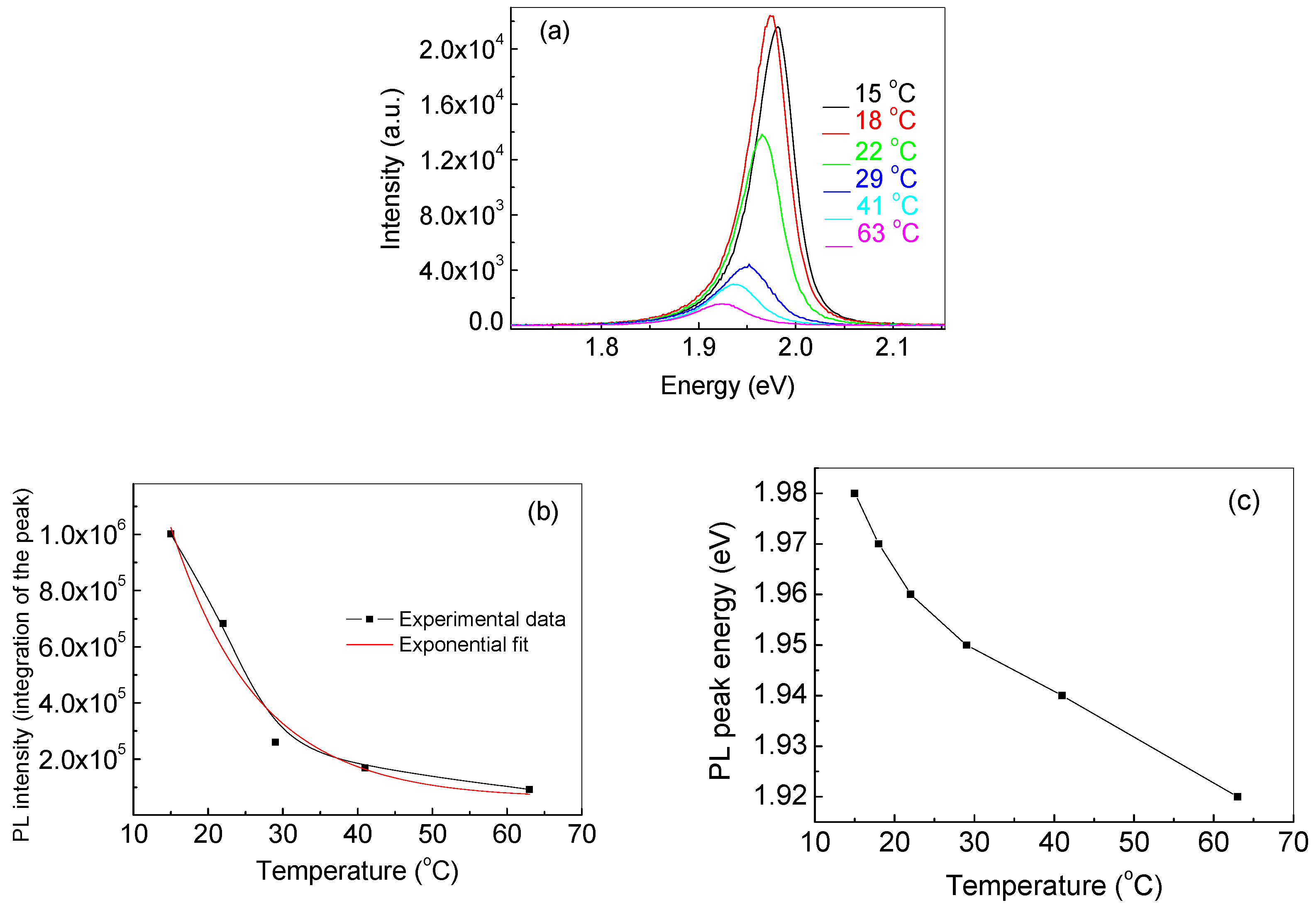
3.2. Temperature Dependence of the PL

For the investigation of the in situ PL under different temperatures, we heated the WS2 monolayer from 15 to 63 °C by a temperature-controlled heater.
Figure 5a displays the PL spectra as a function of the temperature. The PL intensity decreases with the increasing temperature as shown in Figure 5b. The intensity measured at 63 °C was reduced to 6% of the initial value. The curve in Figure 5b is fitted by an exponential function (Equation (1)).
I   ( T ) =   3.5 × 10 7 exp ( 0.085 T )   +   5.9 × 10 4
where, the I is the PL intensity and T is the temperature. The reason behind the exponential behavior will be reported in a future work. Note that the value measured at 18 °C is larger than that at 15 °C. We suspect the exception is possibly due to the experimental error.
Kim et al. [4] found the PL intensity of the WS2 monolayer was reduced after annealing at 800 °C. They suggested the decrease of the PL intensity is attributed to the reduction of the number of the excitons. Su et al. observed the thermal quenching of the WS2 monolayer in the range of room temperature to 400 °C [23]. They attributed the thermal quenching to the thermal activation of nonradiative recombination processes. In addition, they found the strong interaction between the WS2 and the substrate could quench the PL, and pointed out that the interfacial effect may play an important role in the understanding of the 2D materials behavior. Besides the abovementioned possible mechanisms, we suspect another possible reason for the thermal quenching is related to the dipole moment.
In addition to the quenching, the red shift of the PL energy is clearly observed. The PL peak energy reduced from 1.98 to 1.92 eV as temperature increased from 15 to 63 °C with an average rate of ~−1.2 meV/°C. Strain is reported as a possible reason for the energy shift [23]. If there is strain in the sample, the Raman peak position should shift. Figure 6a shows the Raman spectra of WS2 monolayer under different temperatures. The Raman spectra were normalized using the Si peak. However, we found no obvious Raman shift of the A1g mode in Figure 6a. The Raman spectra were measured near room temperature, and the small variation of the temperature may not cause an evident strain, even with a Raman shift. Therefore, we are not sure whether the strain has an effect on the PL energy shift. However, the Raman data in Figure 6b clearly show that the intensity of A1g has a positive proportional linear function with the temperature, indicating the out-of-plane dipole moment increases with the increase of the temperature. As the dipole moment has an effect on the exciton energy, we suspected the increased dipole moment resulted in the PL energy redshift [24]. Furthermore, the increased dipole moment may promote the energy transfer or charge transfer from the excitons to substrate or defects in WS2, resulting the PL quenching.

4. Conclusions

In summary, we have successfully prepared WS2 monolayer in the presence of H2O vapor deposition, suggesting that H2O vapor could be used as a transport agent for the growth of WS2. The AFM, Raman, and PL revealed that monolayer WS2 with triangular shape was formed. Using XRD, we showed that tungsten oxides were formed by the reaction between WS2 and water, which promoted the growth of WS2. By heating the WS2 monolayer, we showed the PL energy and intensity are sensitive to the temperature. The increased dipole moment and energy or charge transfer may be possible reasons for the PL spectra change.

Author Contributions

Y.L. conceived and designed the experiments and analyzed the data; F.H., L.Z. and J.W. performed the experiments; Z.J. analyzed the data; S.Z. wrote the paper.

Funding

This work was funded by the Natural Science Foundation of Zhejiang Province, China Projects (LY16E020008) and Chinese NSF Projects (61106100).

Conflicts of Interest

The authors declare no conflict of interest.

References

  1. Zhang, Y.; Zhang, Y.F.; Ji, Q.Q.; Ju, J.; Yuan, H.T.; Shi, J.P.; Gao, T.; Ma, D.L.; Liu, M.X.; Chen, Y.B.; et al. Controlled growth of high-quality monolayer WS2 layers on sapphire and imaging its grain boundary. ACS Nano 2013, 7, 8963–8971. [Google Scholar] [CrossRef] [PubMed]
  2. Gutierrez, H.R.; Perea-Lopez, N.; Elias, A.L.; Berkdemir, A.; Wang, B.; Lv, R.; Lopez-Urias, F.; Crespi, V.H.; Terrones, H.; Terrones, M. Extraordinary room-temperature photoluminescence in triangular WS2 monolayers. Nano Lett. 2013, 13, 3447–3454. [Google Scholar] [CrossRef] [PubMed]
  3. Yun, S.J.; Chae, S.H.; Kim, H.; Park, J.C.; Park, J.H.; Han, G.H.; Lee, J.S.; Kim, S.M.; Oh, H.M.; Seok, J.; et al. Synthesis of centimeter-scale monolayer tungsten disulfide film on gold foils. ACS Nano 2015, 9, 5510–5519. [Google Scholar] [CrossRef] [PubMed]
  4. Kim, M.S.; Yun, S.J.; Lee, Y.; Seo, C.; Han, G.H.; Kim, K.K.; Lee, Y.H.; Kim, J. Biexciton emission from edges and grain boundaries of triangular WS2 monolayers. ACS Nano 2016, 10, 2399–2405. [Google Scholar] [CrossRef] [PubMed]
  5. Gordo, V.O.; Balanta, M.A.G.; Gobato, Y.G.; Covre, F.S.; Galeti, H.V.A.; Iikawa, F.; Couto, O.D.D., Jr.; Qu, F.; Henini, M.; Hewak, D.W.; et al. Revealing the nature of low-temperature photoluminescence peaks by laser treatment in Van der Waals epitaxially grown WS2 monolayers. Nanoscale 2018, 10, 4807–4815. [Google Scholar] [CrossRef] [PubMed]
  6. Rosenberger, M.R.; Chuang, H.J.; McCreary, K.M.; Li, C.H.; Jonker, B.T. Electrical characterization of discrete defects and impact of defect density on photoluminescence in monolayer WS2. ACS Nano 2018, 12, 1793–1800. [Google Scholar] [CrossRef] [PubMed]
  7. Yao, H.; Liu, L.; Wang, Z.; Li, H.; Chen, L.; Pam, M.E.; Chen, W.; Yang, H.Y.; Zhang, W.; Shi, Y. Significant photoluminescence enhancement in WS2 monolayers through Na2S treatment. Nanoscale 2018, 10, 6105–6112. [Google Scholar] [CrossRef] [PubMed]
  8. Feng, S.; Cong, C.X.; Peimyoo, N.; Chen, Y.; Shang, J.Z.; Zou, C.J.; Cao, B.C.; Wu, L.S.; Zhang, J.; Eginligil, M.; et al. Tunable excitonic emission of monolayer WS2 for the optical detection of DNA nucleobases. Nano Res. 2018, 11, 1744–1754. [Google Scholar] [CrossRef]
  9. Xu, D.Y.; Xu, P.T.; Zhu, Y.Z.; Peng, W.C.; Li, Y.; Zhang, G.L.; Zhang, F.B.; Mallouk, T.E.; Fan, X.B. High yield exfoliation of WS2 crystals into 1–2 layer semiconducting nanosheets and efficient photocatalytic hydrogen evolution from WS2/CdS nanorod composites. ACS Appl. Mater. Interfaces 2018, 10, 2810–2818. [Google Scholar] [CrossRef] [PubMed]
  10. Groven, B.; Heyne, M.; Mehta, A.N.; Bender, H.; Nuytten, T.; Meersschaut, J.; Conard, T.; Verdonck, P.; Van Elshocht, S.; Vandervorst, W.; et al. Plasma-enhanced atomic layer deposition of two-dimensional WS2 from WF6, H2 plasma, and H2S. Chem. Mater. 2017, 29, 2927–2938. [Google Scholar] [CrossRef]
  11. Sahu, R.; Radhakrishnan, D.; Vishal, B.; Negi, D.S.; Sil, A.; Narayana, C.; Datta, R. Substrate induced tuning of compressive strain and phonon modes in large area MoS2 and WS2 van der Waals epitaxial thin films. J. Cryst. Growth 2017, 470, 51–57. [Google Scholar] [CrossRef]
  12. Bae, S.; Kim, H.; Lee, Y.; Xu, X.F.; Park, J.S.; Zheng, Y.; Balakrishnan, J.; Lei, T.; Kim, H.R.; Song, Y.I.; et al. Roll-to-roll production of 30-inch graphene films for transparent electrodes. Nat. Nanotechnol. 2010, 5, 574–578. [Google Scholar] [CrossRef] [PubMed]
  13. Zhao, S.C.; Surwade, S.P.; Li, Z.T.; Liu, H.T. Photochemical oxidation of CVD-grown single layer graphene. Nanotechnology 2012, 23, 355703. [Google Scholar] [CrossRef] [PubMed]
  14. Zhao, S.C.; Zhou, F.; Li, Z.T.; Liu, H.T. Effect of precursor purity and flow rate on the CVD growth of hexagonal boron nitride. J. Alloys Compd. 2016, 688, 1006–1012. [Google Scholar] [CrossRef]
  15. Cong, C.X.; Shang, J.Z.; Wu, X.; Cao, B.C.; Peimyoo, N.; Qiu, C.; Sun, L.T.; Yu, T. Synthesis and optical properties of large-area single-crystalline 2D semiconductor WS2 monolayer from chemical vapor deposition. Adv. Opt. Mater. 2014, 2, 131–136. [Google Scholar] [CrossRef]
  16. Gao, Y.; Liu, Z.B.; Sun, D.M.; Huang, L.; Ma, L.P.; Yin, L.C.; Ma, T.; Zhang, Z.Y.; Ma, X.L.; Peng, L.M.; et al. Large-area synthesis of high-quality and uniform monolayer WS2 on reusable Au foils. Nat. Commun. 2015, 6, 8569. [Google Scholar] [CrossRef] [PubMed]
  17. Li, S.; Wang, S.; Tang, D.; Zhao, W.; Xu, H.; Chu, L.; Bando, Y.; Golberg, D.; Eda, G. Halide-assisted atmospheric pressure growth of large WSe2 and WS2 monolayer crystals. Appl. Mater. Today 2015, 1, 60–66. [Google Scholar] [CrossRef]
  18. Zhao, S.C.; Weng, J.X.; Jin, S.Z.; Lv, Y.F.; Ji, Z.G. Chemical vapor transport deposition of molybdenum disulfide layers using H2O vapor as the transport agent. Coatings 2018, 8, 78. [Google Scholar] [CrossRef]
  19. Ma, Y.D.; Dai, Y.; Guo, M.; Niu, C.W.; Lu, J.B.; Huang, B.B. Electronic and magnetic properties of perfect, vacancy-doped, and nonmetal adsorbed MoSe2, MoTe2 and WS2 monolayers. Phys. Chem. Chem. Phys. 2011, 13, 15546–15553. [Google Scholar] [CrossRef] [PubMed]
  20. Peimyoo, N.; Shang, J.Z.; Cong, C.X.; Shen, X.N.; Wu, X.Y.; Yeow, E.K.L.; Yu, T. Nonblinking, intense two-dimensional light emitter: Mono layer WS2 triangles. ACS Nano 2013, 7, 10985–10994. [Google Scholar] [CrossRef] [PubMed]
  21. Chow, P.K.; Jacobs-Gedrim, R.B.; Gao, J.; Lu, T.M.; Yu, B.; Terrones, H.; Koratkar, N. Defect-induced photoluminescence in monolayer semiconducting transition metal dichalcogenides. ACS Nano 2015, 9, 1520–1527. [Google Scholar] [CrossRef] [PubMed]
  22. Stier, A.V.; McCreary, K.M.; Jonker, B.T.; Kono, J.; Crooker, S.A. Exciton diamagnetic shifts and valley Zeeman effects in monolayer WS2 and MoS2 to 65 Tesla. Nat. Commun. 2016, 7, 10643. [Google Scholar] [CrossRef] [PubMed]
  23. Su, L.Q.; Yu, Y.F.; Cao, L.Y.; Zhang, Y. Effects of substrate type and material-substrate bonding on high-temperature behavior of monolayer WS2. Nano Res. 2015, 8, 2686–2697. [Google Scholar] [CrossRef]
  24. Motta, C.; Mandal, P.; Sanvito, S. Effects of molecular dipole orientation on the exciton binding energy of CH3NH3PbI3. Phys. Rev. B 2016, 94, 045202. [Google Scholar] [CrossRef]
Figure 1. (a) Optical microscopy image of tungsten disulfide monolayer. (b) Corresponding photoluminescence (PL) mapping. The multilayer was circled in (a,b). (c) Photoluminescence (PL) spectrum of the tungsten disulfide monolayer, which was taken from the monolayer region labelled with a box in (a)/(b). The spectrum was fitted with Lorentzian function (green lines). The peaks at 2.00 and 1.98 eV are due to the transition of charged and defect-related excitons, respectively. The scale bars represent 50 μm.
Coatings 08 00205 g001
Figure 2. Atomic force microscopy (AFM) image (a) and the corresponding cross-section (b) (along the blue line marked in (a)) of monolayer WS2 grown on the SiO2/Si substrate.
Coatings 08 00205 g002
Figure 3. Typical Raman spectrum of the WS2 monolayer.
Coatings 08 00205 g003
Figure 4. X-ray diffraction (XRD) of WS2 powder after annealing in Ar/H2 and H2O vapor at 1000 °C for 20 h. The peak positions are indexed to tungsten oxides W18O49 (JCPDS No. 05-0392 and No. 65-5468).
Coatings 08 00205 g004
Figure 5. (a) Photoluminescence (PL) spectra of the WS2 monolayer measured at different temperatures, showing the decrease of intensity and redshift of the PL energy with the rising temperatures. (b) Integrated PL intensity as a function of temperature. The PL intensity was calculated by integration from 1.8 to 2.1 eV. The curve was fit with an exponential function (red line). (c) Temperature dependence of the PL peak energy.
Coatings 08 00205 g005
Figure 6. (a) Raman spectra of the WS2 monolayer at different temperatures. The Raman spectra were normalized using the Si peak. (b) Integrated Raman intensity of A1g mode as a function of temperature. The intensity was calculated by integration from 400 to 434 cm−1. The curve was fit with a linear function (red line).
Coatings 08 00205 g006

