Solution-Processed Efficient Nanocrystal Solar Cells Based on CdTe and CdS Nanocrystals

 ,
,
Abstract
:
1. Introduction
2. Experiment Procedure
2.1. Materials
2.2. Synthesis Methods
2.3. Device Fabrication
3. Results and Discussion
4. Conclusions
Supplementary Materials
Acknowledgments
Author Contributions
Conflicts of Interest
References
- Kim, J.Y.; Voznyy, O.; Zhitomirsky, D.; Sargent, E.H. Colloidal quantum dot materials and devices: A quarter-century of advances. Adv. Mater. 2013, 25, 4986–5010. [Google Scholar] [CrossRef] [PubMed]
- Kagan, C.R.; Lifshitz, E.; Sargent, E.H.; Talapin, D.V. Building devices from colloidal quantum dots. Science 2016, 353, aac5523. [Google Scholar] [CrossRef] [PubMed]
- Xue, H.; Wu, R.; Xie, Y.; Tan, Q.; Qin, D.; Wu, H.; Huang, W. Recent progress on solution-processed CdTe nanocrystals solar cells. Appl. Sci. 2016, 6, 197. [Google Scholar] [CrossRef]
- Chen, G.; Ning, Z.; Agren, H. Nanostructured Solar Cells. Nanomaterials 2016, 6, 145. [Google Scholar] [CrossRef] [PubMed]
- Paulo, S.; Palomares, E.; Martinez-Ferrero, E. Graphene and carbon quantum dot-based materials in photovoltaic devices: From synthesis to applications. Nanomaterials 2016, 6, 157. [Google Scholar] [CrossRef] [PubMed]
- Maloney, F.S.; Poudyal, U.; Chen, W.; Wang, W. Influence of quantum dot concentration on carrier transport in ZnO:TiO2 nano-hybrid photoanodes for quantum dot-sensitized solar cells. Nanomaterials 2016, 6, 191. [Google Scholar] [CrossRef] [PubMed]
- Wu, R.; Yang, Y.; Li, M.; Qin, D.; Zhang, Y.; Hou, L. Solvent engineering for high-performance PbS quantum dote solar cells. Nanomaterials 2017, 7, 201. [Google Scholar] [CrossRef] [PubMed]
- Yang, Y.; Zhao, B.; Gao, Y.; Liu, H.; Tian, Y.; Qin, D.; Wu, H.; Huang, W.; Hou, L. Novel hybrid ligands for passivating PbS colloidal quantum dots to enhance the performance solar cells. Nano-Micro Lett. 2015, 7, 325–331. [Google Scholar] [CrossRef]
- Wu, H.; Zhang, X.; Zhang, Y.; Yan, L.; Gao, W.; Zhang, T.; Wang, Y.; Zhao, J.; Yu, W.W. Colloidal PbSe Solar Cells with Molybdenum Oxide Modified Graphene Anodes. ACS Appl. Mater. Interfaces 2015, 7, 21082–21088. [Google Scholar] [CrossRef] [PubMed]
- Zhu, J.; Yang, Y.; Gao, Y.; Qin, D.; Wu, H.; Hou, L.; Huang, W. Enhancement of open-circuit voltage and the fill factor in CdTe nanocrystal solar cells by using inferface materials. Nanotechnology 2014, 25, 365203. [Google Scholar] [CrossRef] [PubMed]
- Li, M.; Liu, X.; Wen, S.; Liu, S.; Heng, J.; Qin, D.; Hou, L.; Wu, H.; Xu, W.; Huang, W. CdTe Nanocrystal Hetero-Junction Solar Cells with High Open Circuit Voltage Based on Sb-doped TiO2 Electron Acceptor Materials. Nanomaterials 2017, 7, 101. [Google Scholar] [CrossRef] [PubMed]
- Dharmadasa, I.M.; Madugu, M.L.; Olusola, O.I.; Echendu, O.K.; Fauzi, F.; Diso, D.G.; Weerasinghe, A.R.; Druffel, T.; Dharmadasa, R.; Lavery, B.; et al. Electroplating of CdTe thin films from cadmium sulphate precursor and comparison of layers grown by 3-electrode and 2-electrode systems. Coatings 2017, 7, 17. [Google Scholar] [CrossRef]
- Kim, K.; Eo, Y.J.; Cho, A.; Gwak, J.; Yun, J.H.; Shin, K.; Ahn, S.K.; Park, S.H.; Yoon, K.; Ahn, S. Role of chelate complexes in densification of CuInSe2 (CIS) thin film prepared from amorphous Cu-In-Se nanoparticle precursors. J. Mater. Chem. 2012, 22, 8444–8448. [Google Scholar] [CrossRef]
- Hahn, J.S.; Park, G.; Lee, J.; Shim, J. Synthesis of CuInSe2 nanoparticles in an oleic acid solution for application in thin film solar cells. J. Ind. Eng. Chem. 2015, 21, 754–759. [Google Scholar] [CrossRef]
- Britt, J.; Ferekides, C. Thin-film CdS/CdTe solar cell with 15.8% efficiency. Appl. Phys. Lett. 1993, 62, 2851–2852. [Google Scholar] [CrossRef]
- Dharmadasa, I.M.; Ojo, A.A.; Salim, H.I.; Dharmadasa, R. Next generation solar cells based on graded bandgap device structures utilizing rod-type nano-materials. Energies 2015, 8, 5440–5458. [Google Scholar] [CrossRef]
- Acharya, S.; Bangera, K.V.; Shivakumar, G.K. Electrical characterization of vacuum-deposited p-CdTe/n-ZnSe heterojunctions. Appl. Nanosci. 2015, 5, 1003–1007. [Google Scholar] [CrossRef]
- Liu, B.; Luo, R.; Liang, Q.; Zheng, Y.; Li, B.; Zhang, J.; Li, W.; Wu, L.; Feng, L. Preparation of novel CdS/ZnS composite window layer for CdTe thin film solar cell. J. Mater. Sci. Mater. Electron. 2015, 26, 9985–9990. [Google Scholar] [CrossRef]
- Horsley, K.; Beal, R.J.; Wilks, R.G.; Blum, M.; Häming, M.; Hanks, D.A.; Weir, M.G.; Hofmann, T.; Weinhardt, L.; Bär, M.; et al. Impact of annealing on the chemical structure and morphology of the thin-film CdTe/ZnO interface. J. Appl. Phys. 2014, 116, 024312. [Google Scholar] [CrossRef]
- Green, M.A.; Emery, K.; Hishikawa, Y.; Warta, W.; Dunlop, E.D.; Levi, D.H.; Ho-Baillie, A.W.Y. Solar cell efficiency tables (version 49). Prog. Photovolt. Res. Appl. 2017, 25, 3–13. [Google Scholar] [CrossRef]
- Burst, J.M.; Duenow, J.N.; Albin, D.S.; Colegrove, E.; Reese, M.O.; Aguiar, J.A.; Jiang, C.-S.; Patel, M.K.; Al-Jassim, M.M.; Kuciauskas, D.; et al. CdTe solar cells with open-circuit voltage breaking the 1 V barrier. Nat. Energy 2016, 15, 16051. [Google Scholar] [CrossRef]
- Gur, I.; Fromer, N.A.; Geier, M.L.; Alivisators, A.P. Air-stable all-inorganic nanocrystal solar cells processed from solution. Science 2005, 310, 462–465. [Google Scholar] [CrossRef] [PubMed]
- Xie, Y.; Tan, Q.; Zhang, Z.; Lu, K.; Li, M.; Xu, W.; Qin, D.; Zhang, Y.; Hou, L.; Wu, H. Improving performance in CdTe/CdSe nanocrystal solar cells by using bulk nano-heterojunctions. J. Mater. Chem. C 2016, 4, 6483–6491. [Google Scholar] [CrossRef]
- Liu, H.; Tian, Y.; Zhang, Y.; Gao, K.; Lu, K.; Wu, R.; Qin, D.; Wu, H.; Peng, Z.; Hou, L.; et al. Solution processed CdTe/CdSe nanocrystal solar cells with more than 5.5% efficiency by using an inverted device structure. J. Mater. Chem. C 2015, 3, 4227–4234. [Google Scholar] [CrossRef]
- Anderson, I.E.; Breeze, A.J.; Olson, J.D.; Yang, L.; Sahoo, Y.; Carter, S.A. All-inorganic spin-cast nanoparticle solar cells with nonselective electrodes. Appl. Phys. Lett. 2009, 94, 063101. [Google Scholar] [CrossRef]
- Wen, S.; Li, M.; Yang, J.; Mei, X.; Wu, B.; Liu, X.; Heng, J.; Qin, D.; Hou, L.; Xu, W.; et al. Rationally controlled synthesis of CdSexTe1−x alloy nanocrystals and their application in efficient graded bandgap solar cells. Nanomaterials 2017, 7, 380. [Google Scholar] [CrossRef] [PubMed]
- MacDonald, B.I.; Martucci, A.; Rubanov, S.; Wakins, S.E.; Mulvaney, P.; Jasieniak, J.J. Layer-by-layer assembly of sintered CdSexTe1−x nanocrystal solar cells. ACS Nano 2012, 6, 5995–6004. [Google Scholar] [CrossRef] [PubMed]
- Jasieniak, J.; MacDonald, B.I.; Wakins, S.E.; Mulvaney, P. Solution-processed Sintered Nanocrystal Solar Cells via Layer-by-Layer Assembly. Nano Lett. 2011, 11, 2856–2864. [Google Scholar] [CrossRef] [PubMed]
- Kumar, S.G.; Rao, K.S.R.K. Physics and chemistry of CdTe/CdS thin film heterojunction photovoltaic devices: Fundamental and critical aspects. Energy Environ. Sci. 2014, 7, 45–102. [Google Scholar] [CrossRef]
- Zhang, H.; Kurley, J.M.; Russell, J.C.; Jang, J.; Talapin, D.V. Solution-processed, ultrathin solar cells from CdCl3−-capped CdTe nanocrystals: The multiple roles of CdCl3− ligands. J. Am. Chem. Soc. 2016, 138, 7464–7467. [Google Scholar] [CrossRef] [PubMed]
- Panthani, M.G.; Kurley, J.M.; Crisp, R.W.; Dietz, T.C.; Ezzyat, T.; Luther, J.M.; Talapin, D.V. High efficiency solution processed sintered CdTe nanocrystal solar cells: The role of interfaces. Nano Lett. 2014, 14, 670–675. [Google Scholar] [CrossRef] [PubMed]
- Macdonald, B.I.; Gengenbach, T.R.; Watkins, S.E.; Mulvaney, P.; Jasieniak, J.J. Solution-processing of ultra-thin CdTe/ZnO nanocrystal solar cells. Thin Solid Films 2014, 558, 365–373. [Google Scholar] [CrossRef]
- Chen, Z.; Zhang, H.; Zen, Q.; Wang, Y.; Xu, D.; Wang, L.; Wang, H.; Yang, B. In Situ Construction of nanoscale CdTe-CdS bulk heterojunctions for inorganic nanocrystal solar cells. Adv. Energy Mater. 2014, 4, 1400235. [Google Scholar] [CrossRef]
- Chen, Z.; Zeng, Q.; Liu, F.; Jin, G.; Du, X.; Du, J.; Zhang, H.; Yang, B. Efficient inorganic solar cells from aqueous nanocrystals: The impact of composition on carrier dynamics. RSC Adv. 2015, 5, 74263–74269. [Google Scholar] [CrossRef]
- Tian, Y.; Zhang, Y.; Lin, Y.; Gao, K.; Zhang, Y.; Liu, K.; Yang, Q.; Zhou, X.; Qin, D.; Wu, H.; et al. Solution-processed efficient CdTe nanocrystal/CBD-CdS hetero-junction solar cells with ZnO interlayer. J. Nanopart. Res. 2013, 15, 2053. [Google Scholar] [CrossRef]
- Crisp, R.W.; Panthani, M.G.; Rance, W.L.; Duenow, J.N.; Parilla, P.A.; Callahan, R.; Dabney, M.S.; Berry, J.J.; Talapin, D.V.; Luther, J.M. Nanocrystal grain growth and device architectures for high-efficiency CdTe ink-based photovoltaics. ACS Nano 2014, 8, 9063–9072. [Google Scholar] [CrossRef] [PubMed]
- Crisp, R.W.; Pach, G.F.; Kurley, J.M.; France, R.M.; Reese, M.O.; Nanayakkara, S.U.; Macleod, B.A.; Talapin, D.V.; Beard, M.C.; Luther, J.M. Tandem solar cells from solution-processed CdTe and PbS quantum dots using a ZnTe-ZnO tunnel junction. Nano Lett. 2017, 17, 1020–1027. [Google Scholar] [CrossRef] [PubMed]
- Cao, Y.; Wang, J. One-pot Synthesis of high-quality zinc-blende CdS nanocrystals. J. Am. Chem. Soc. 2004, 126, 14336–14337. [Google Scholar] [CrossRef] [PubMed]
- Peng, Z.A.; Peng, X. Formation of high-quality CdTe, CdSe, and CdS nanocrystals using CdO as precurssor. J. Am. Chem. Soc. 2001, 123, 183–184. [Google Scholar] [CrossRef] [PubMed]
- Li, Z.; Ji, Y.; Xie, R.; Grisham, S.Y.; Peng, X. Correlation of CdS Nanocrystal Formation with Elemental Sulfur Activation and Its Implication in Synthetic Development. J. Am. Chem. Soc. 2011, 133, 17248–17256. [Google Scholar] [CrossRef] [PubMed]
- Yong, K.; Sahoo, Y.; Swihart, M.T.; Prasad, P.N. Shape control of CdS nanocrystals in one-pot synthesis. J. Phys. Chem. C 2007, 111, 271–273. [Google Scholar] [CrossRef]
- Chu, H.; Li, X.; Chen, G.; Zhou, W.; Zhang, Y.; Jin, Z.; Xu, J.; Li, Y. Shape-controlled synthesis of CdS nanocrystals in mixed solvents. Cryst. Growth Des. 2005, 5, 1801–1806. [Google Scholar] [CrossRef]
- Yu, W.; Peng, X. Formation of high-quality CdS and other II–VI semiconductor nanocrystals in noncoordinating solvents: Tunable reactivity of monomers. Angew. Chem. Int. Ed. 2002, 41, 2368–2371. [Google Scholar] [CrossRef]
- Duffy, N.W.; Peter, L.M.; Wang, R.L. Characterisation of CdS/CdTe heterojunctions by photocurrent spectroscopy and electroreflectance/absorbance spectroscopy (EEA/EER). J. Electroanal. Chem. 2002, 532, 207–214. [Google Scholar] [CrossRef]
- Han, J.; Liao, C.; Jiang, T.; Spanheimer, C.; Haindl, G.; Fu, G.; Krishnakumar, V.; Zhao, K.; Klein, A.; Jaegermann, W. An optimized multilayer structure of CdS layer for CdTe solar cells application. J. Alloys Compd. 2011, 509, 5285–5289. [Google Scholar] [CrossRef]
- Lin, H.; Xia, W.; Wu, H.; Tang, C. CdS/CdTe solar cells with MoOx as back contact buffers. Appl. Phys. Lett. 2010, 97, 123504. [Google Scholar] [CrossRef]
- Yun, J.H.; Cha, E.S.; Ahn, B.T.; Kwon, H.; Al-Ammar, E.A. Performance improvement in CdTe solar cells by modifying the CdS/CdTe interface with a Cd treatment. Curr. Appl. Phys. 2014, 14, 630–635. [Google Scholar] [CrossRef]
- Xiao, D.; Li, X.; Wang, D.; Li, Q.; Shen, K.; Wang, D. CdTe thin film solar cell with NiO as a back contact buffer layer. Sol. Energy Mater. Sol. Cells 2017, 169, 61–67. [Google Scholar] [CrossRef]
- Spalatu, N.; Hiie, J.; Mikli, V.; Krunks, M.; Valdna, V.; Maticiuc, N.; Raadik, T.; Caraman, M. Effect of CdCl2 annealing treatment on structural and optoelectronic properties of close spaced sublimation CdTe/CdS thin film solar cells vs deposition conditions. Thin Solid Films 2015, 582, 128–133. [Google Scholar] [CrossRef]
- Chu, T.-Y.; Song, O.-K. Hole mobility of N,N′-bis(naphthalen-1-yl)-N,N′-bis(phenyl) benzidine investigated by using space-charge-limited currents. Appl. Phys. Lett. 2007, 90, 203512. [Google Scholar] [CrossRef]
- Meysing, D.M.; Wolden, C.A.; Griffith, M.M.; Mahabaduge, H.; Pankow, J.; Reese, M.O.; Burst, J.M.; Rance, W.L.; Barnes, T.M. Properties of Reactively Sputtered Oxygenated Cadmium Sulfide (CdS:O) and Their Impact on CdTe Solar Cell Performance. J. Vac. Sci. Technol. A Vac. Surf. Films 2015, 33, 021203. [Google Scholar] [CrossRef]
- Varkey, A.J.; Fort, A.F. Transparent conducting cadmium oxide thin films prepared by a solution growth technique. Thin Solid Films 1994, 239, 211–213. [Google Scholar] [CrossRef]


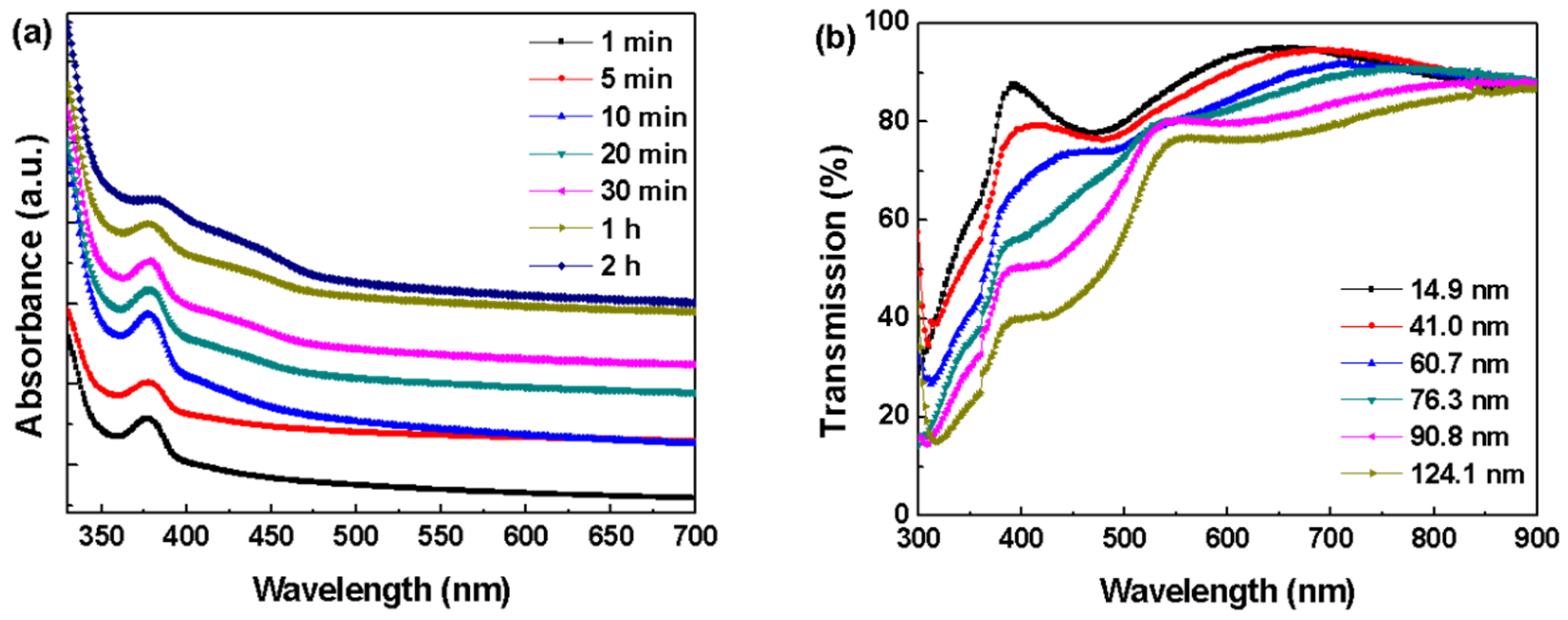
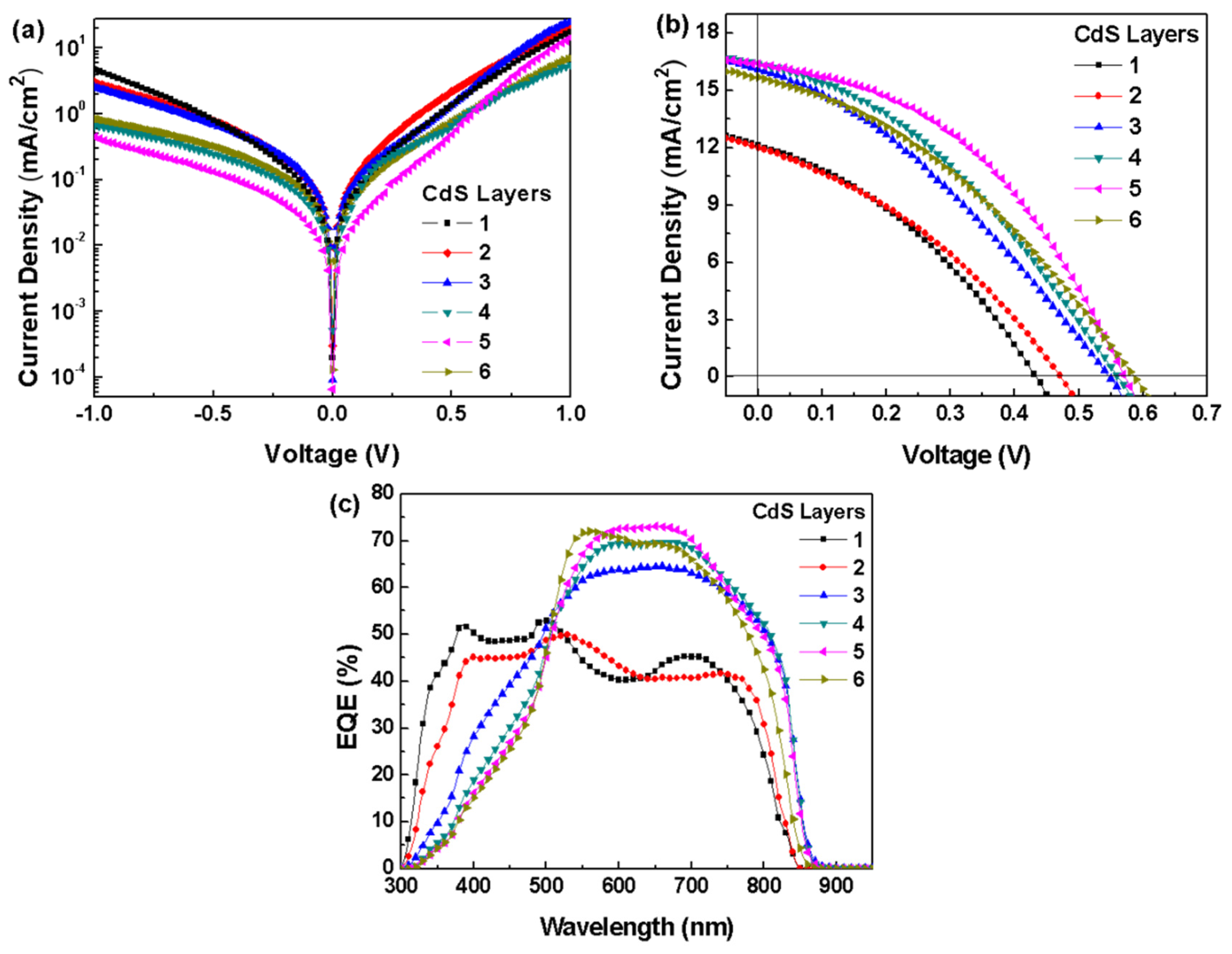
| CdS Layer | Thickness (nm) | Voc (V) | Jsc (mA/cm2) | FF (%) | PCE (%) | (Ω·cm2) | (Ω·cm2) |
|---|---|---|---|---|---|---|---|
| 1 | 14.9 | 0.43 | 12.14 | 35.84 | 1.87 | 19.4 | 94.0 |
| 2 | 41.0 | 0.47 | 11.98 | 34.79 | 1.96 | 21.7 | 88.0 |
| 3 | 60.7 | 0.55 | 16.15 | 32.72 | 2.91 | 23.6 | 91.7 |
| 4 | 76.3 | 0.56 | 16.39 | 36.28 | 3.33 | 21.4 | 138.0 |
| 5 | 90.8 | 0.57 | 16.36 | 42.74 | 3.98 | 15.4 | 213.6 |
| 6 | 124.1 | 0.59 | 15.66 | 35.40 | 3.27 | 22.3 | 136.9 |
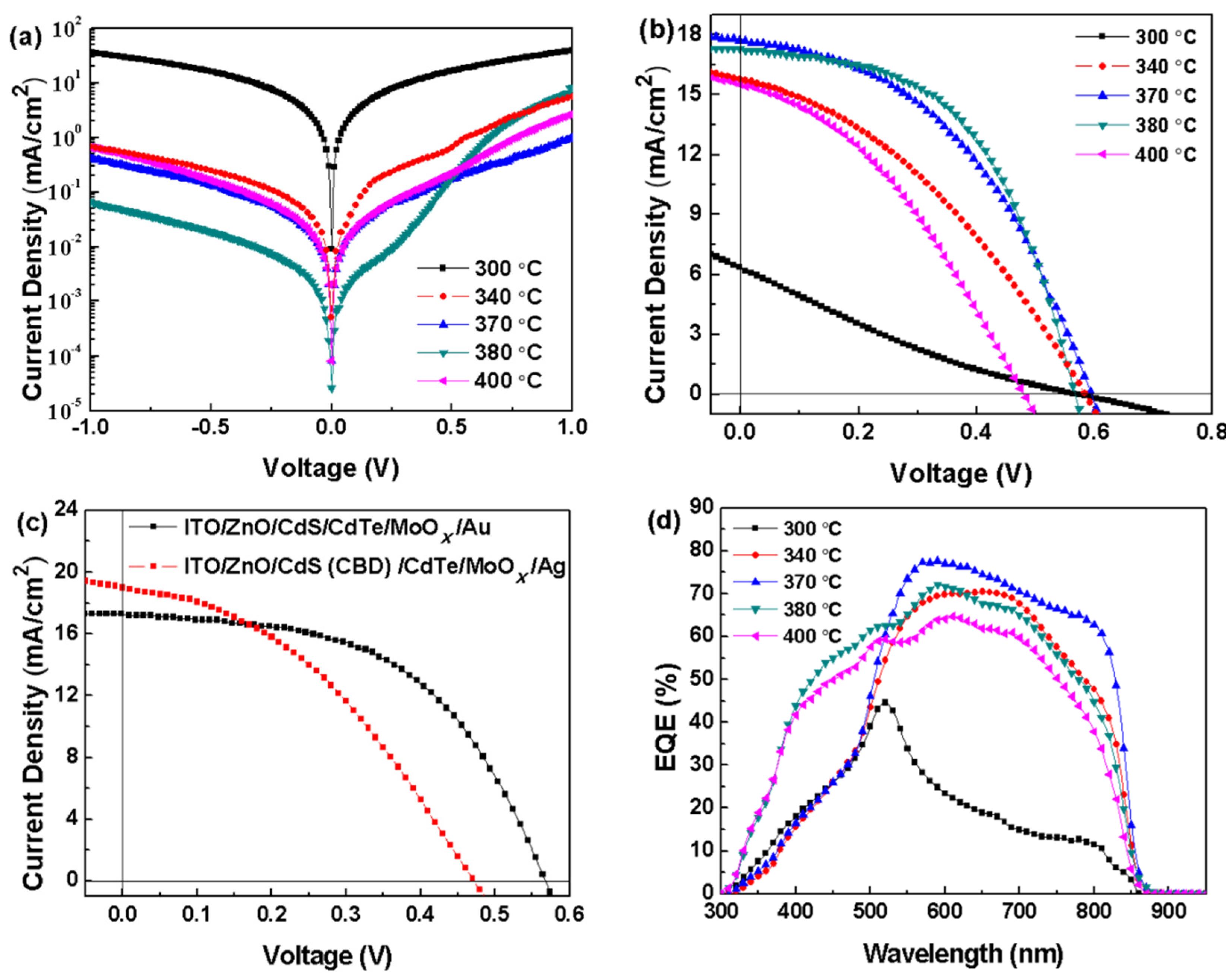
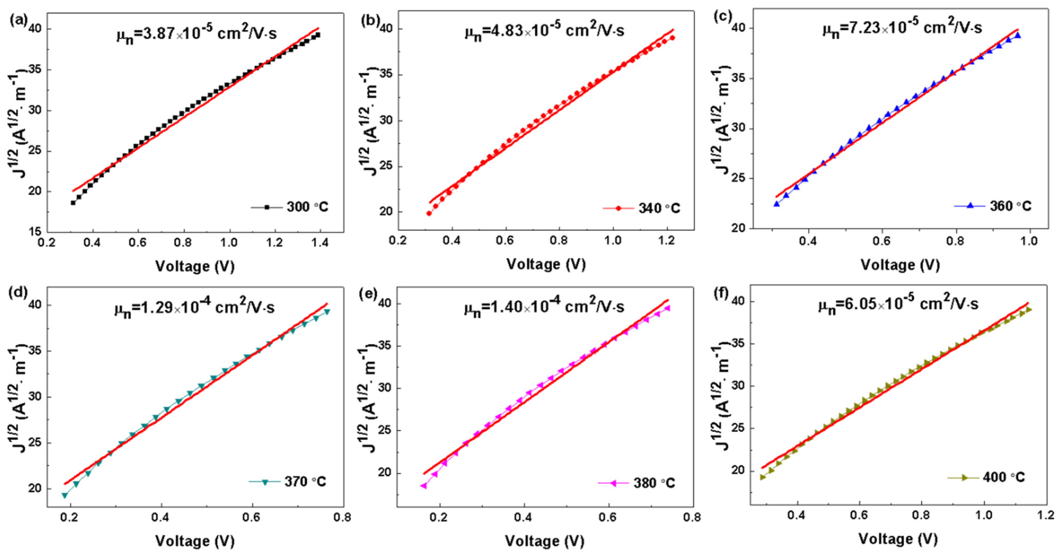
| Annealing Temperature | Hole Mobility (cm2·V−1·s−1) |
|---|---|
| 300 °C | 3.87 × 10⁻⁵ |
| 340 °C | 4.83 × 10⁻⁵ |
| 360 °C | 7.23 × 10⁻⁵ |
| 370 °C | 1.29 × 10⁻⁴ |
| 380 °C | 1.40 × 10⁻⁴ |
| 400 °C | 6.05 × 10⁻⁵ |
| CdS Film | Annealing Temperature | Voc (V) | Jsc (mA/cm2) | FF (%) | PCE (%) |
|---|---|---|---|---|---|
| NC | 300 °C | 0.57 | 6.36 | 19.73 | 0.72 |
| NC | 340 °C | 0.59 | 15.79 | 36.45 | 3.40 |
| NC | 370 °C | 0.59 | 17.69 | 44.63 | 4.69 |
| NC | 380 °C | 0.56 | 17.26 | 52.84 | 5.14 |
| NC | 400 °C | 0.48 | 15.54 | 36.39 | 2.74 |
| CBD | 380 °C | 0.52 | 17.36 | 48.60 | 3.61 |
© 2018 by the authors. Licensee MDPI, Basel, Switzerland. This article is an open access article distributed under the terms and conditions of the Creative Commons Attribution (CC BY) license (http://creativecommons.org/licenses/by/4.0/).
Share and Cite
Liu, S.; Liu, W.; Heng, J.; Zhou, W.; Chen, Y.; Wen, S.; Qin, D.; Hou, L.; Wang, D.; Xu, H. Solution-Processed Efficient Nanocrystal Solar Cells Based on CdTe and CdS Nanocrystals. Coatings 2018, 8, 26. https://doi.org/10.3390/coatings8010026
Liu S, Liu W, Heng J, Zhou W, Chen Y, Wen S, Qin D, Hou L, Wang D, Xu H. Solution-Processed Efficient Nanocrystal Solar Cells Based on CdTe and CdS Nanocrystals. Coatings. 2018; 8(1):26. https://doi.org/10.3390/coatings8010026
Chicago/Turabian StyleLiu, Songwei, Weigeng Liu, Jingxuan Heng, Wenfeng Zhou, Yanru Chen, Shiya Wen, Donghuan Qin, Lintao Hou, Dan Wang, and Hui Xu. 2018. "Solution-Processed Efficient Nanocrystal Solar Cells Based on CdTe and CdS Nanocrystals" Coatings 8, no. 1: 26. https://doi.org/10.3390/coatings8010026
APA StyleLiu, S., Liu, W., Heng, J., Zhou, W., Chen, Y., Wen, S., Qin, D., Hou, L., Wang, D., & Xu, H. (2018). Solution-Processed Efficient Nanocrystal Solar Cells Based on CdTe and CdS Nanocrystals. Coatings, 8(1), 26. https://doi.org/10.3390/coatings8010026