1. Introduction
Titanium dioxide is an important material in optical applications due to its high refractive index, high hardness and chemical resistance. It plays important role in solar control [
1], self-cleaning [
2], anti-reflective and low emissivity (Low-E) coatings. Low-E coatings are applied to large area architectural glazing to reduce heat losses from buildings. They combine high visible transparency with high reflectance in the far-infrared region. To achieve this combination of properties, Low-E coatings generally consist of dielectric-silver-dielectric multi-layer systems or stacks, where the thin (~10 nm) silver layer reflects long wavelength IR back into the building and the dielectric layers both protect the silver and act as anti-reflectance layers [
3]. Titania is commonly used as the dielectric layer [
4] and all the layers are usually deposited by magnetron sputtering, which is considered to be one of the most important large-area coating technologies [
5,
6]. The market for low-E coatings has grown considerably in recent years due to environmental legislation and increased energy costs. To further expand the market, the next generation of Low-E coatings are increasingly being deposited onto toughenable glass, which is post-deposition annealed at temperatures of up to 650 °C. However, titania can exist in a number of crystalline forms with different properties and the final structure is dependent on both the deposition conditions and any post-deposition treatments [
7]. Titania coatings usually form amorphous, anatase, rutile or mixed phase structures (a third phase, brookite, is rarely found in thin films). The refractive index increases from
n < 2.3 at 550 nm for an amorphous film to
n > 2.6 at 550 nm for a pure rutile phase film. Thus, the toughening process could potentially change the structure and therefore the proprieties, of the titania layers, which in turn could have a detrimental impact on the performance of the Low-E stack.
Many different techniques can be used to deposit TiO
2 such as sol-gel process [
8,
9,
10], chemical vapour deposition [
11,
12,
13,
14,
15], ion beam depositions [
16], and magnetron sputtering [
17,
18,
19,
20,
21]. In this project the latter technique has been used to produce titania coatings, which were post-deposition annealed over a range of temperatures to allow their subsequent structural development to be investigated.
2. Experimental Section
Titanium dioxide films were deposited onto 4 mm thick soda-lime glass by reactive pulsed DC magnetron sputtering. Films were sputtered from standard planar magnetrons using a 99.5% purity metal target of a dimensions of 100 mm × 300 mm, driven by an Advanced Energy Pinnacle Plus power supply operating in pulsed DC mode at an average power of 1 kW and a pulse frequency of 100 kHz and 5.0 µsec off time (i.e., 50% duty). The optical emission monitoring (OEM) system was used to control the amount of oxygen introduced into the system during films deposition. The optimal conditions were found to be when the OEM signal was set to 20% of the full metal signal. Argon gas was introduced into the chamber by a mass flow controller (MKS Instruments Ltd., Andover, MA, USA), and was set at 65 standard cubic centimetres per minute (SCCM). Coatings were deposited at a pressure of about 0.2 Pa and the substrate-magnetron separation was about 90 mm.
Selected samples were post deposition annealed in air in the range 200–700 °C for 10 min and analysed by a wide range of techniques to determine film morphology, composition and crystalline structure.
The coating thickness was measured by a Dektak® 3M stylus profilometer (Vecco Instruments Inc., Plainview, TX, USA) and was determined to be close to 1.5 µm in all cases.
The crystallographic proprieties of the film were performed using Bragg- Brentano mode on a Siemens D5000 Diffractometer D7 with Cu Kα radiation and Ni filter and Scintillation detector. The angular step of the sample rotation in respect to the incident beam is 0.1° and counting time is 15 s/step.
Raman spectroscopy (Renishaw inVia spectrometer with 514.4 nm wavelength of argon ion laser, Wotton-under-Edge, UK) was also carried out to further investigate the crystalline structure of the titania coatings before and after annealing as a comparison to the XRD analysis.
The surface morphology of the titanium dioxide coatings was investigated using scanning electron microscopy (SEM, Supra 40VP, Carl Zeiss GmbH, Munich, Germany ) operating at 1–3 kV and atomic force microscopy (AFM, MultiMode™ SPM with Nanoscope III controller with the WSXM software, Digital Instruments, Santa Barbara, CA, USA). Energy dispersive X-ray analysis with 40 mm2 silicon drift detector (Trident, EDAX Inc., Mahwah, NJ, USA) with an electron beam energy of 8 keV was used to determine the stoichiometry of the deposited materials.
3. Results and Discussion
Titania samples deposited in this work were post-deposition annealed in the range 200–700 °C for 10 min in air. Selected samples were investigated by EDX analysis to determine the coating composition. The results suggest that samples deposited in this work show almost stoichiometric compositions of TiO2 consisting of 34 at% (61 wt %) of Ti and 66 at% (39 wt %) of O2.
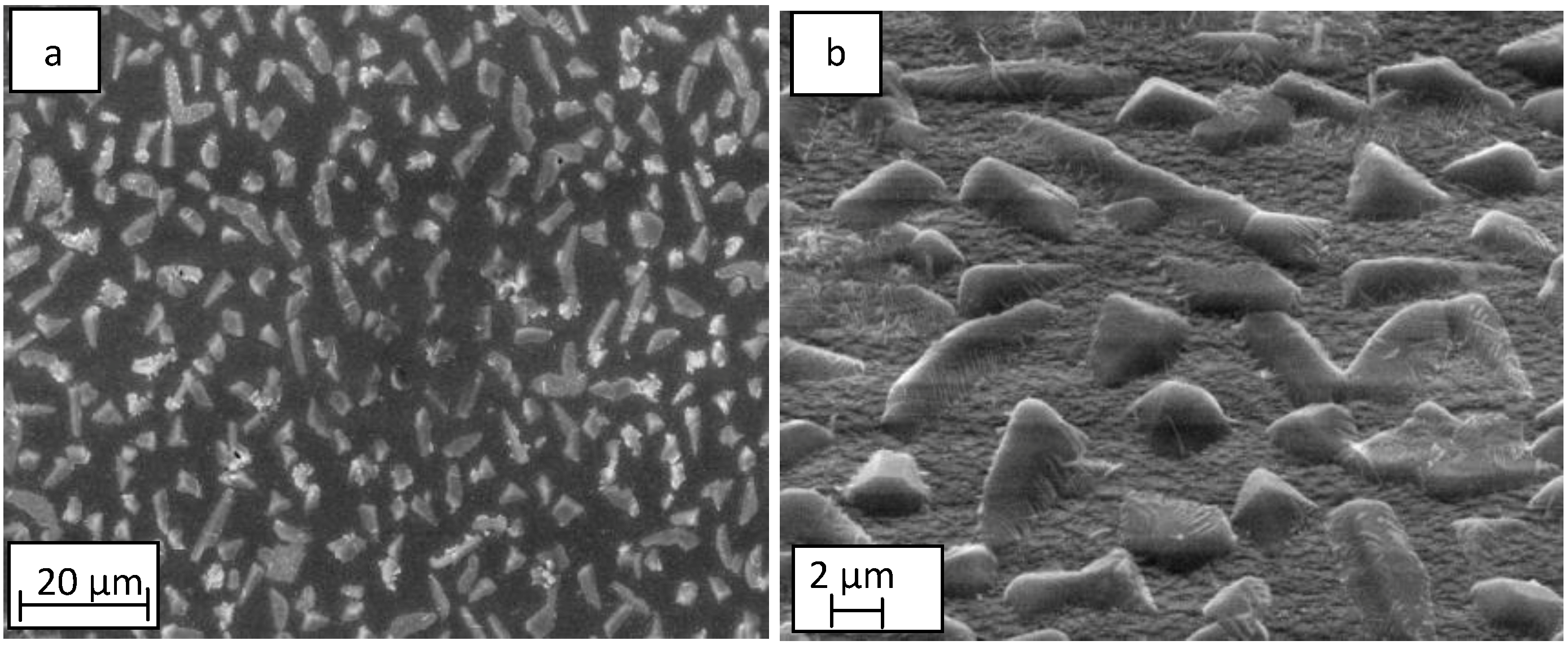
SEM analysis was carried out to investigate film morphology. The image shown in
Figure 1 presents the fracture section of the as-deposited sample. The coating has a dense structure and a reasonably smooth surface morphology, with some small defects existing on the surface.
Micro-Raman spectroscopy was performed to investigate changes in the crystalline structure of the titania coatings after annealing. Titanium dioxide can form three main crystalline structures: tetragonal anatase and rutile, which belong to the space group
![Coatings 03 00166 i001]()
and
![Coatings 03 00166 i002]()
, respectively, and lower symmetry orthorhombic brookite (
D2h space group representation) [
22,
23]. Factor group analysis of anatase indicates the existence of 15 optical modes with the following representation of normal vibrations: 1A
1g + 1A
2u + 2B
1g + 1B
2u + 3E
g + 2E
u [
24]. Within this representation 1A
1g, 2B
1g, 3E
g are Raman active, whereas the remaining modes are active in Infrared [
24].
Figure 1.
SEM images of the fracture section of as-deposited titania sample deposited onto float glass substrate.
Figure 1.
SEM images of the fracture section of as-deposited titania sample deposited onto float glass substrate.
Raman analysis gives information about the nature of the bonds in a structure and there is substantial evidence indicating that the peak position, shape and intensity of Raman peaks are related to sub-stoichiometric defects, quantum confinement effects, crystal sizes, nanocrystallinity and large interfacial areas [
22,
23,
25,
26]. Spectra obtained from the titania films produced in this work were compared against those obtained for pure titania nano-crystals to allow any variations in phase, stoichiometry or degree of crystallisation in the analysed films to be identified.
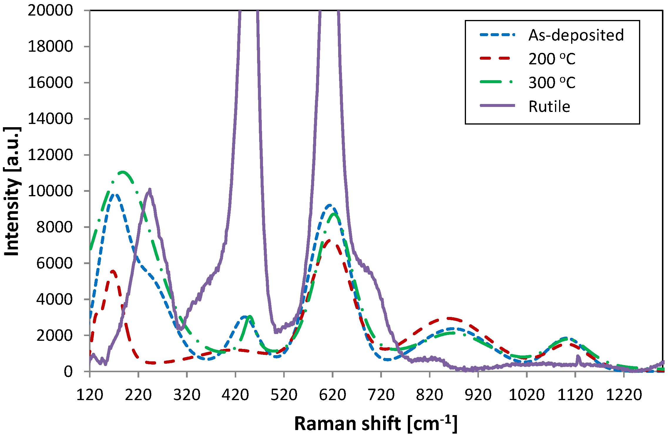
Figure 2 represents Raman spectra taken from the as-deposited sample, and samples annealed at 200 °C and 300 °C. The spectrum from a nanocrystalline rutile standard (standards provided by Cristal Global, Stallingborough, UK) is also included in the figure showing two characteristic Raman shifts at 447 and 612 cm
−1. The samples show relatively low intensity peaks shifted to lower and higher numbers at 447 cm
−1 and 612 cm
−1, respectively. The rutile shoulder peak at 237 cm
−1 in all the samples is overlaid with a lower Raman shift peak situated at about 185 cm
−1, which may indicate a mixture of anatase and brookite formation. Anatase is represented by a high intensity peak at 144 cm
−1 and a weak peak at 197 cm
−1, whereas brookite shows a strong shift at 153 cm
−1. Moreover, in the sample annealed at 200 °C the peak at 447 cm
−1 has significantly decreased, showing a low intensity broad peak. This implies that even though peak positions in these samples are characteristic to crystalline rutile formation there is no long range ordering in these samples and the Raman shifts are most likely represented by amorphous vibrations. It has been suggested that peak broadening occurs due to nanocrystallinity and quantum confinement effects, and that there is a characteristic dependency between grain size and peak position and broadening in Raman analysis [
23,
25,
26,
27]. Finally Li Bassi
et al. [
22] pointed out that materials with smaller particles (~4.4 nm) have Raman spectrum similar to that of amorphous materials, which could also be the case here.
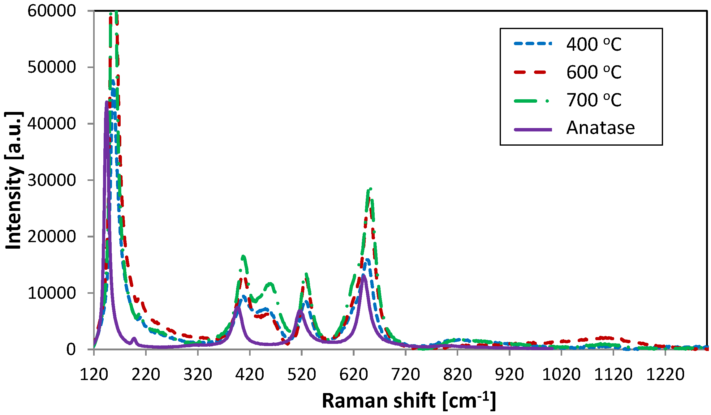
Figure 3 presents samples annealed at 400 °C, 600 °C and 700 °C aligned with an anatase nanocrystalline powder standard (characteristic Raman shifts at 144, 399, 515 and 639 cm
−1). For all these samples a distinct anatase structure can be seen. Samples annealed at the temperature range of 400–700 °C show the degradation of the rutile-like structure in favour of very strong anatase peaks formation.
Figure 2.
Raman spectra of titania coatings from the as-deposited sample and samples annealed at 200 and 300 °C, aligned with the rutile standard.
Figure 2.
Raman spectra of titania coatings from the as-deposited sample and samples annealed at 200 and 300 °C, aligned with the rutile standard.
Figure 3.
Raman spectra collected from samples annealed at 400, 600 and 700 °C and anatase standard.
Figure 3.
Raman spectra collected from samples annealed at 400, 600 and 700 °C and anatase standard.
Moreover, a peak at about 460 cm
−1 that appears in these analysed samples probably indicates the presence of the rutile phase in the crystal structure. This peak increases with rising annealing temperature. Additionally, in the case of sample annealed at 700 °C a weak shoulder is presented at 620 cm
−1, which also represents one of the characteristic shifts in the rutile structure. This may suggest that the titania structure is shifting from anatase to the rutile phase, which would be expected since rutile tends to form in highly energetic processes, therefore high temperature annealing may initiate the rutile forming process. Some quite significant peak up shifting and broadening was detected, which could be caused by non-stoichiometric composition of the material or by small particle sizes [
23]. The broad, weak peaks at about 1100 cm
−1 arise from the glass surface, as found by Xie
et al. [
28].
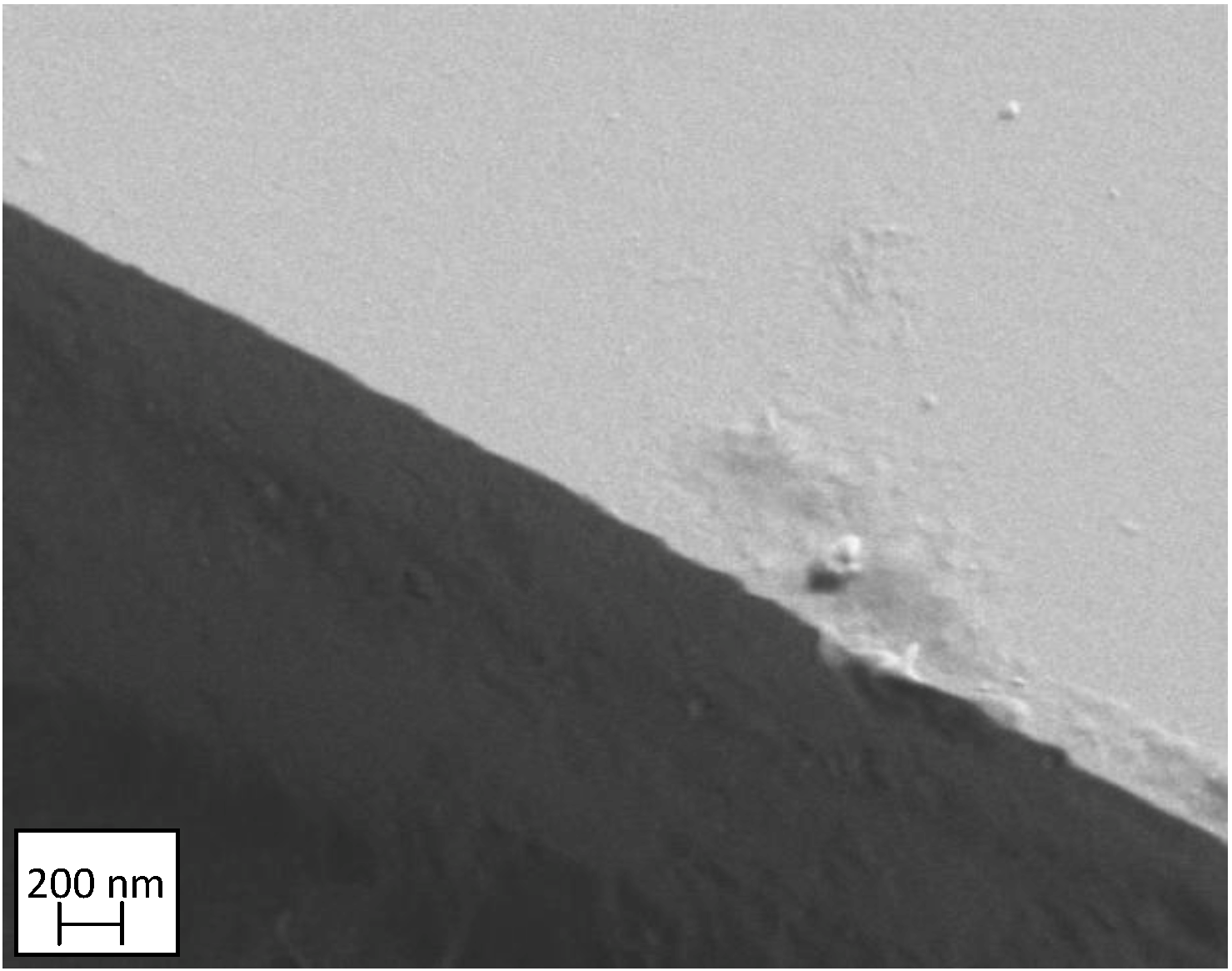
To investigate the structural changes at higher temperatures one additional sample was annealed at 700 °C for 10 min in air. SEM micrographs presented in
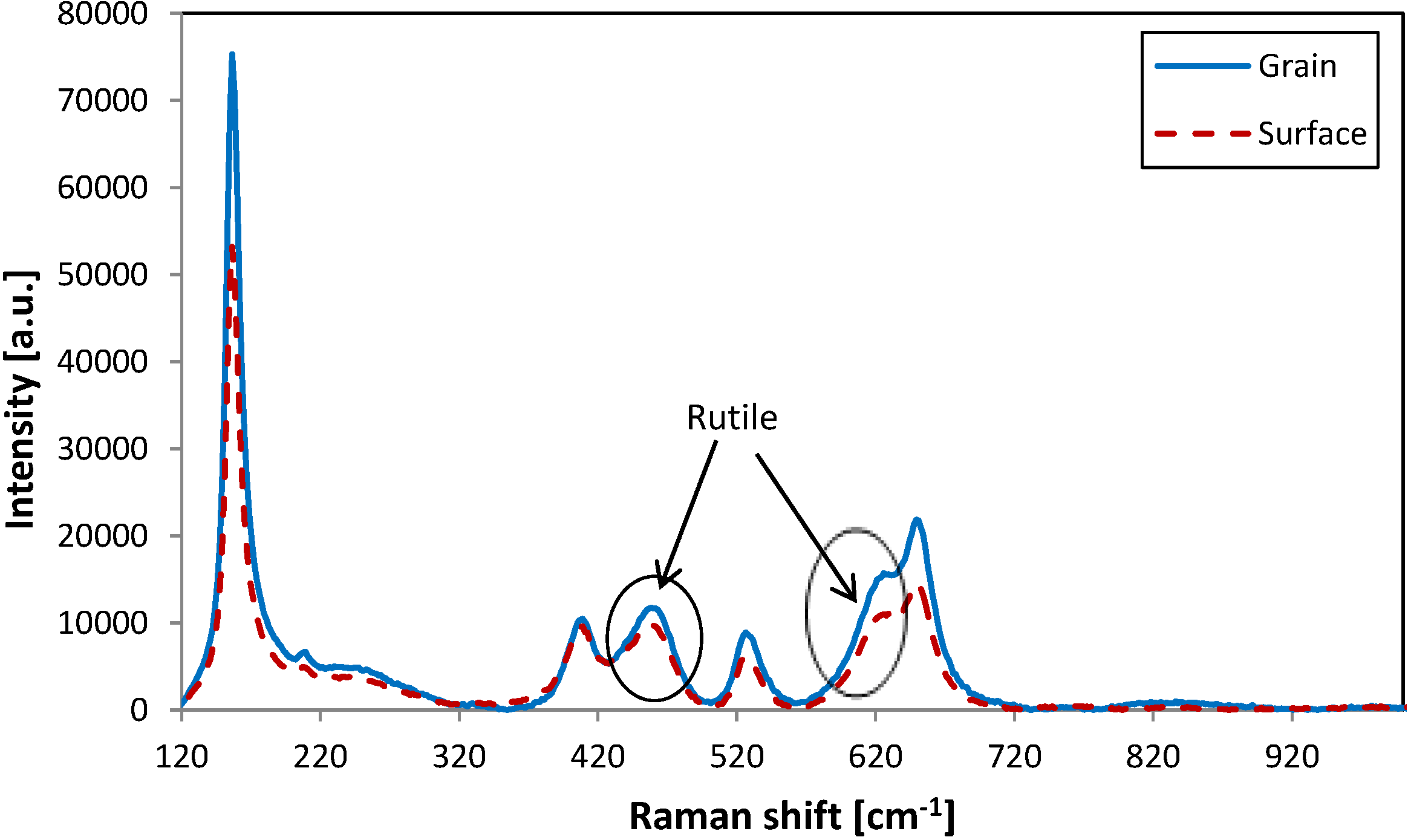
Figure 4a,b show visible changes in the surface topography. Features on the film surface appear to have been caused by post deposition crystallisation processes after treatment at relatively high temperature. To compare if there is any difference in crystal structure between the surface region and the features observed by SEM, Raman scans were taken from the faceted area and the surrounding surface region, respectively (see
Figure 5). In both cases analysis showed that the crystalline structure was the same, but there are differences in peak intensities. It may suggest that these regions have the same crystal structure as the surrounding surface. On the other hand, micro-Raman is not a surface specific technique, and the laser, which penetrates to a depth of about 1 µm, picks up signals not just from the sample surface but also from regions underneath.
Figure 4.
SEM micrograph of the surface of the titania sample, deposited onto float glass and annealed at 700 °C: (a) at lower magnification scan and (b) at higher magnification scan.
Figure 4.
SEM micrograph of the surface of the titania sample, deposited onto float glass and annealed at 700 °C: (a) at lower magnification scan and (b) at higher magnification scan.
Figure 5.
Raman images of sample annealed at 700 °C. Red-collected from surface, blue-from grain.
Figure 5.
Raman images of sample annealed at 700 °C. Red-collected from surface, blue-from grain.
Figure 5 shows the Raman spectra obtained from both surface and faceted region of the sample annealed at 700 °C. Both scans present the same shapes for the Raman peaks (same shifts detected), however they differ slightly in the intensities. This may be due to higher concentration of the detected mixed anatase/rutile crystals in the grain areas, as sharper and more intensive peaks indicate higher crystallinity. This suggests that the grains are regions of improved crystallinity, which arose during the high temperature treatment. Following that, the spectrum obtained from the sample annealed at 700 °C for 10 min shows mixed anatase/rutile structure. A strong peak at 445 cm
−1 wavelength and peak shoulder at 615 cm
−1 is indicative of a rutile structure, which is known to be formed by higher energy processes; therefore increasing temperature allows a transformation to occur from meta-stable anatase to rutile [
17]. Unfortunately, further investigations of titania films phase transformation due to high temperature treatment was restricted by the glass substrate properties, which softens when annealed at temperatures above 700 °C.
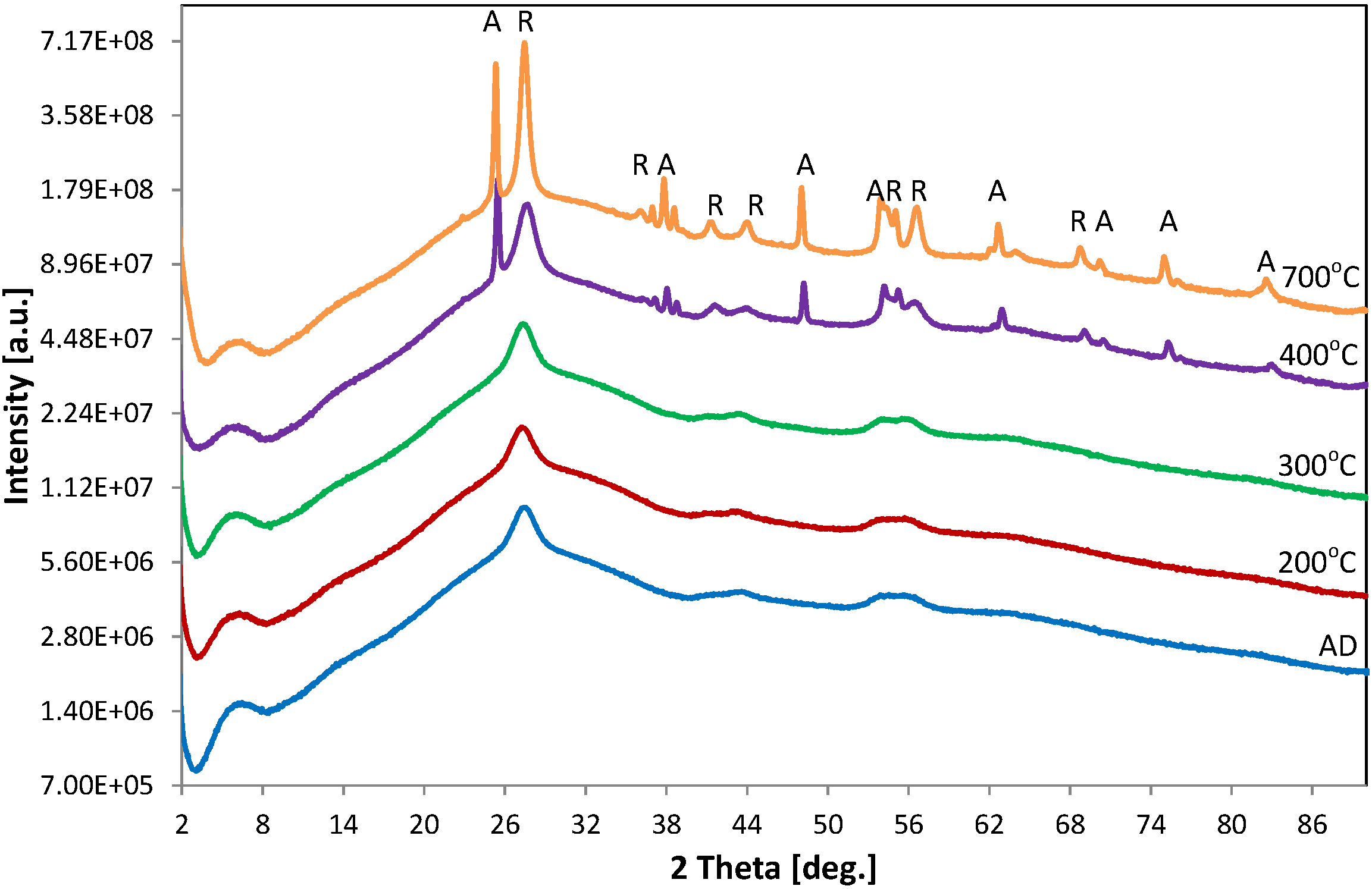
The XRD analysis was carried out to determine the crystalline structure of titania coatings. The analysis was carried out on an as-deposited TiO
2 sample and samples annealed at 200, 300, 400 and 700 °C.
Figure 6 shows the diffraction patterns obtained from these samples.
Figure 6.
XRD diffractograms collected from TiO2 as-deposited sample and annealed at 200, 300, 400 and 700 °C for 10 min. Lines represent peak position for anatase (red) and rutile (black) phases, respectively.
Figure 6.
XRD diffractograms collected from TiO2 as-deposited sample and annealed at 200, 300, 400 and 700 °C for 10 min. Lines represent peak position for anatase (red) and rutile (black) phases, respectively.
XRD analysis indicates that samples treated at temperatures below 400 °C show an unknown or weakly crystalline phase, which could be rutile-based. This structure has been determined as consisting of a very small grain size (~3 nm). In samples annealed at 400 °C and above, evidence for a two-phase anatase and rutile structure can be distinguished. In addition, based on the peak widths, the crystallite size for anatase is much larger than for rutile, which could be the reason why in the Raman analysis it was detected more easily than rutile in samples annealed at 400–600 °C.
Finally, the XRD results show that the sample annealed at 700 °C consists of mixed anatase/rutile phases in the coatings, similar to what was found from Raman analysis for this sample. Nevertheless, Raman spectra collected from samples annealed at relatively high temperatures (400–600 °C) suggested that anatase is the leading form of titania presented in these samples. This may be caused by the significant difference in the grain sizes between rutile and anatase. As mentioned earlier, particle sizes are one of the main factors that influence Raman analysis as well as XRD. Generally, relatively small grains represent broader, lower intensity peaks, which furthermore in Raman may also cause peak shifting. Therefore, if the anatase has significantly larger grains than the rutile in titania coatings characterised in this study it could be picked up as a dominant phase in Raman spectroscopy.
Table 1 shows the grain sizes calculated using the full width half maximum of the peaks from the Debye-Scherrer equation [
29].
Table 1.
Crystallite size calculated for titania samples characterised by XRD.
Table 1.
Crystallite size calculated for titania samples characterised by XRD.
| Sample | Crystallite size (110) Rutile [nm] | Crystallite size (101) Anatase [nm] | Crystallite size Amorphous Phase [nm] |
|---|
| AD | – | – | 3.3 |
| 200 °C | – | – | 3.4 |
| 300 °C | – | – | 3.5 |
| 400 °C | 4.7 | 77 | – |
| 700 °C | 14 | 110 | – |
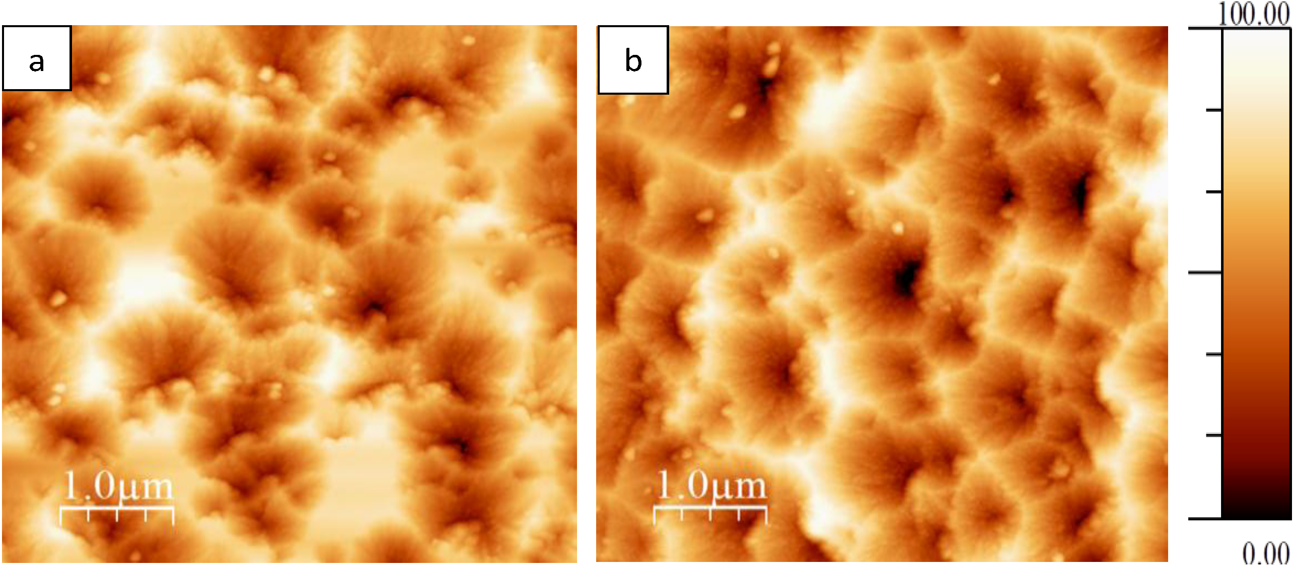
In order to investigate surface roughness atomic force microscopy (AFM) analysis was conducted. Surface roughness was investigated in the as-deposited sample and the sample annealed at 600 °C for 10 min.
Figure 7 shows 5 µm × 5 µm images of the surface topography of these coating.
Table 2 shows root-mean-square (RMS) and roughness average (Ra) values for both samples. The values are slightly higher for the as-deposited sample, which suggests that during heat treatment grain sizes increase, filling the free spaces and/or valleys on the coating surface, and hence surface roughness decreases in the annealed film. However, the difference in roughness values is not very large, therefore it should not influence coating performance.
Figure 7.
(a) AFM image collected from as-deposited titania sample; (b) AFM image collected from titania sample post-deposition annealed at 600 °C deposited onto float glass substrate.
Figure 7.
(a) AFM image collected from as-deposited titania sample; (b) AFM image collected from titania sample post-deposition annealed at 600 °C deposited onto float glass substrate.
Table 2.
Roughness average and root-mean-square values obtained from AFM analysis for as-deposited and annealed at 600 °C titania samples.
Table 2.
Roughness average and root-mean-square values obtained from AFM analysis for as-deposited and annealed at 600 °C titania samples.
| TiO2 sample | Ra [nm] | RMS [nm] |
|---|
| As-deposited | 13.8 | 16.9 |
| Annealed at 600 °C | 13.1 | 16.4 |


 ,
, 
 and
and  , respectively, and lower symmetry orthorhombic brookite (D2h space group representation) [22,23]. Factor group analysis of anatase indicates the existence of 15 optical modes with the following representation of normal vibrations: 1A1g + 1A2u + 2B1g + 1B2u + 3Eg + 2Eu [24]. Within this representation 1A1g, 2B1g, 3Eg are Raman active, whereas the remaining modes are active in Infrared [24].


