Article

In2S3/C3N4 Nanocomposite and Its Photoelectric Properties in the Broadband Light Spectrum Range

1
School of Environmental and Material Engineering, Center of Advanced Functional Materials, Yantai University, Yantai 264005, China
2
National Laboratory of Industrial Control Technology, Institute of Cyber-Systems and Control, Zhejiang University, Hangzhou 310027, China
*
Author to whom correspondence should be addressed.
Coatings 2025, 15(6), 718; https://doi.org/10.3390/coatings15060718
Submission received: 20 May 2025 / Revised: 11 June 2025 / Accepted: 13 June 2025 / Published: 14 June 2025

Abstract

To extend the spectral utilisation of In2S3, an In2S3/C3N4 nanocomposite was prepared. The effects of different sulphur sources, electrodes, and bias voltages on the optoelectronic performance were examined. Photoelectric properties in response to light sources with wavelengths of 405, 532, 650, 780, 808, 980, and 1064 nm were investigated using Au electrodes and the carbon electrodes with 5B pencil drawings. This study shows that the aggregation states of the In2S3/C3N4 nanocomposite possess photocurrent switching responses in the broadband region of the light spectrum. Combining two types of partially visible light-absorbing material extends utilisation to the near-infrared region. Impurities or defects embody an electron-donating effect. Since the energy levels of defects or impurities with an electron-donating effect are close to the conduction band, low-energy lights (especially NIR) can be utilised. The non-equilibrium carrier concentration (photogenerated electrons) of the nanocomposites increases significantly under NIR photoexcitation conditions. Thus, photoconductive behaviour is manifested. A good photoelectric signal was still measured when zero bias was applied. This demonstrates self-powered photoelectric response characteristics. Different sulphur sources significantly affect the photoelectric performance, suggesting that they create different defects that affect charge transport and base current noise. It is believed that interfacial interactions in the In2S3/C3N4 nanocomposite create a built-in electric field that enhances the separation and transfer of electrons and holes produced by light stimulation. The presence of the built-in electric field also leads to energy band bending, which facilitates the utilisation of the light with longer wavelengths. This study provides a reference for multidisciplinary applications.

1. Introduction

In2S3 belongs to a class of the functional materials that can be used in the visible light region thanks to its band gap width of around 2.3 eV. Expanding its utilisation in the near infrared remains a major challenge. In2S3 and its nanocomposites have been extensively studied and applied in photocatalytic hydrogen evolution [1,2,3,4,5,6,7,8,9,10,11,12,13,14,15,16,17,18,19,20,21], photocatalyst for H2O2 production [22,23], CO2 photoreduction [24,25,26], chemical sensors and biosensors [27,28,29,30,31,32,33,34,35,36], sodium-ions battery [37], lithium-sulphur battery [38], supercapacitors [38], alkali-ion batteries [39], solar cells [40], photodetectors [41,42], photocatalytic fields [43,44,45,46,47,48,49,50,51,52,53,54,55,56,57], optical memristor devices as artificial synapses [58], self-powered response devices [59], etc. The nanocomposite systems involved are In2S3/In2O3 [1,2,4,9,18,27,31,33,51,55], In2S3/In(OH)3/ZnS [3], ZnO/In2S3 [5], indium sulphide/indium oxide/gold [6], In2S3/ZnIn2S4 [7], ZnIn2S4/porphyrin (Cu)-COF heterojunction [10], In2S3/WO3 [11,34], Cd0.8Zn0.2S/In2S3 heterojunction [14], g-C3N4/In2S3 S-scheme heterojunction [15], In2S3/Fe2V4O13 [21], MnIn2S4@In2S3 [22], In2S3/Cu2S heterojunction [24], TiO2@In2S3 hybrid [25,36,48], copper indium gallium disulfide and indium sulphide on zinc oxide [26], Bi2S3−x/In2S3−y [30], MoS2/In2S3 heterostructure [32], In2S3/CoS2 heterostructure [37], graphene/In2S3 nanostructure [38], In2S3/ZnS [45], FeVO4/In2S3 [46], g-C3N4/BiVO4/In2S3 [47], In2S3/Ag2S heterostructures [49], CeO2/TiO2/In2S3 [50], ZnO/ZnS/In2S3 [53], B-g-C3N4−x@Bi2S3/In2S3 [56], In2S3/Cd0.9Zn0.1S heterojunction [57], CuxInyS/CdS heteronanocrystals [60], sulphur vacancies and palladium doping of In2S3 [8,52], Mo-doped In2S3 [12], Pt/AgInS2/Nafion [16], P-doped In2.77S4 [20], Bi2S3−x with sulphur defects [30], Zn-doped In2S3 [33], Bi-doped In2S3 [41], Fe doping in In2S3 [54,55], etc.
From the above literature analyses, it is clear that improving the physicochemical properties of In2S3 is mainly achieved through heterojunction, doping, interfacial interaction and defect engineering. These measures can alter its electronic structure, thereby enhancing its optical, electrical, and photoelectric properties, and enabling its use in a variety of applications. For example, Li and co-workers [31] constructed hierarchical In2S3@In2O3 heterojunctions. Malathi and co-workers [32] synthesised 2D/2D MoS2/In2S3 heterostructures via interfacial engineering. Zhu and co-workers [37] prepared a defect-rich In2S3/CoS2 heterostructure. Wang and co-workers [52] tailored the sulphur vacancy of In2S3−x. Alagarasan and co-workers [41] fabricated Bi-doped In2S3 for UV photodetector. Guillemeney and co-workers [61] synthesized ultrathin indium sulphide nanoribbons. Kim and co-workers [62] prepared indium sulphide magic size clusters, etc.
Given the wide range of applications of indium sulphide-based nanomaterials, it is important to be able to modify their properties. One important way to design nanocomposites demonstrating excellent performance is to integrate multiple components to achieve the complementarity and synergy of each component through interfacial interactions. Based on the C3N4 structure, which resembles graphene with an abundance of nitrogen (N) elements and defects, the N element is rich in lone-pair electrons. The electron-donating effect of these lone-pair electrons, combined with defect passivation, is expected to significantly enhance the material’s photophysical properties. Additionally, the formation of built-in electric fields in nanocomposites is an intrinsic driving force that helps to prevent photogenerated charge recombination and is an important manifestation of interfacial interactions. This can lead to energy band bending, helping to utilise light with longer wavelengths. Interfacial charge transfer is the root cause of the generation of built-in electric fields. Therefore, this study aims to enhance the photophysical properties of In2S3 by engineering the interactions between In2S3 and C3N4 and by manipulating defects. Strong interfacial charge transfer can significantly enhance the resulting nanocomposites’ optical, electrical, and optoelectronic properties, as well as their multidisciplinary applications.
Since the band gap of C3N4 is approximately 2.7 eV, and it is also one of the materials that utilise part of the visible light. The C3N4-based nanocomposites have been widely developed in the fields of dye-sensitized solar cells [63], photocatalytic CO2 reduction [64,65,66,67,68], photocatalytic hydrogen evolution [69,70], and photocatalysis [71,72,73,74,75,76]. Although most of the references on C3N4-based nanomaterials mainly focus on the photocatalytic field, solar cells, light detection, and photocatalysis have some common key scientific issues. This study provides some useful complementary work from a multidisciplinary perspective. Sharma and co-workers [77] studied solar water splitting in saltwater using In2S3/S-C3N4-dots. Our previous report [78] investigated the interfacial interaction between C3N4 and Fe2O3 and its defect passivation to tailor the photophysical properties. In this contribution, based on the band gap of In2S3 around 2.3 eV, narrowing the band gap of In2S3 with non-metallic elements, such as C, N, S, P, is a general approach. The combination of In2S3 and C3N4 is similar to the C, N co-doped In2S3 material system. Compared to C, N doping or C, N co-doping, C3N4 contains a C, N conjugated unit. This conjugated structure favours charge delocalisation and charge redistribution. For In2S3/C3N4 nanocomposites, the modulation of the electronic effect is mainly achieved through interfacial interactions. Combining two types of visible light-absorbing material is expected to extend absorption into the near-infrared region. Defects play a significant role in enhancing the large redshift of the material. In terms of electronic effects, defects exhibit both donor and acceptor effects. Those with a donor electron effect are near the conduction band, while those with an acceptor electron effect are near the valence band. These defects are beneficial for utilising low-energy light. However, defects with a donor electron effect and defects with an acceptor electron effect lead to different conductive behaviours. This study focuses on the interfacial interactions between In2S3 and C3N4, as well as their photophysical properties in the broadband region. The study focuses on the photogenerated charge transport properties of nanocomposites in an aggregated state. Grain boundaries and interfaces play an important role here. The grain boundaries of the nanocomposite are more complex than its surfaces and interfaces. There are a large number of defects at grain boundaries, and impurities collect there too. These defects and impurities significantly affect the photophysical properties of the nanocomposite. The resulting nanocomposites exhibited photogenerated charge extraction properties from the visible to the near-infrared spectrum when a bias of 0 V was applied. They exhibited self-powered photoelectric response characteristics.
Optoelectronic materials cover a very wide range of areas, such as solar cells, photodetectors, fluorescence, photothermal, photocatalytic, and so on. Among them, photodetectors have many applications in communication, wireless control systems, environmental monitoring, biological and chemical sensors, visual images, image sensors, etc. [79,80,81]. The performance of photodetectors depends not only on the photoelectric materials involved; its device structure is also very important. Their optoelectronic properties are strongly dependent on a variety of interfaces. This is the result of a combination of various factors. These studies of photodetectors provide valuable inspiration and reference for controlling the microstructure of materials, extracting photoelectric signals and for multidisciplinary applications. In particular, the self-driven photodetector devices reported in recent years are one of the important research directions [82,83,84,85,86,87,88,89,90]. The self-powered photoelectric response characteristics provide valuable insights into the interfacial interactions of nanocomposites. Not only do they facilitate the development of low-energy consumption devices, they also inhibit the recombination of photogenerated carriers from the material itself. Efficient interfacial charge transfer is required in the resulting nanocomposites to form a strong built-in electric field that promotes the separation of photogenerated carriers. The strength of this field depends heavily on the interaction between the interfaces. The nanocomposites produced in this study showed photogenerated charge extraction at zero bias, which is a promising development for applications involving low energy consumption. As there are already well-established research teams focusing on photodetectors and solar cells, we do not intend to follow their work. Instead, our aim is to provide cross-cutting and complementary content from a multidisciplinary perspective, focusing on the materials themselves. We hope that this serves as a reference for multidisciplinary fields.

2. Materials and Methods

2.1. Materials

Indium trichloride (AR) (99.9%), Macklin (Shanghai, China). Thiourea (CP, chemical pure) (Greater than 99.0%), Tianjin Taixing Reagent Factory (Tianjin, China). Sodium thiosulfate (AR) (Greater than 99.0%) was provided from Tianjin Guangcheng Chemical Reagent Co., Ltd. (Tianjin, China).

2.2. Preparation of Graphitic Carbon Nitride

Graphitic carbon nitride (C3N4) synthesised is shown in reference [78]. Thiourea was used as raw material and resulted in S-doped C3N4.

2.3. Preparation of the In2S3/C3N4 Nanocomposite

To 20 mL of C3N4 suspensions, 40 mL of H2O, 0.5 g of indium trichloride, and a certain amount of thiourea or sodium thiosulfate as sulphur sources were added. The preparation conditions were 120–130 °C for 8–24 h using the hydrothermal method. The In2S3/C3N4 nanocomposite was obtained. The experimental details can be seen in reference [78].

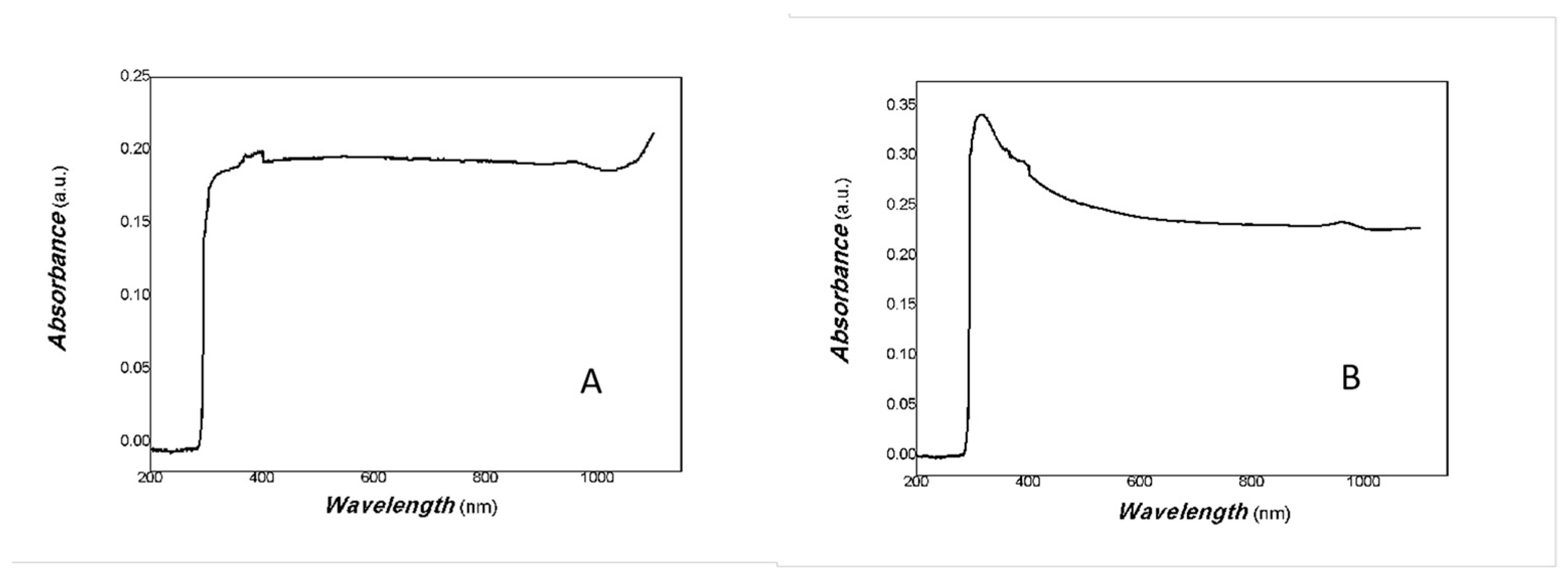
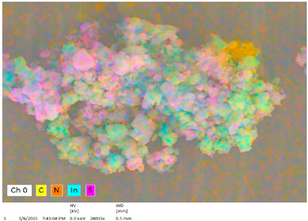
2.4. Characterization of SEM, EDS, EDS Mapping, TEM, UV-Vis-NIR and XRD

The characterisation of scanning electron microscopy (SEM), EDS (Energy Dispersive Spectrometer) and EDS mapping (Quantax XFlash6, manufactured by Bruker, Germany) (Karlsruher, Germany), the TEM (transmission electron microscope), UV-Vis-NIR (UV-VIS-NIR spectrophotometer), and XRD (X-ray powder diffraction) was shown in the reference [78]. SEM and EDS mapping were used with ZEISS Gemini SEM300 (Jena, Germany). EDS and EDS mapping were carried out by EDS scanning installed in SEM (ZEISS Gemini SEM300), detecting some such as In, S, C, N, or other reasonable atoms (AI and O). TEM was carried out with JEM-1011 (Japan Electronics Co., Ltd., Tokyo, Japan). UV-Vis-NIR was carried out with a TU-1810 spectrophotometer (Beijing Puxi General Instrument Co., Ltd., Beijing, China). The XRD experiment was taken with XRD-7000 from SHIMADZU (Shimadzu, Kyoto, Japan), respectively. In order to eliminate the interference of nuclear electric effect, the resulting nanocomposites were coated on the aluminium foil during SEM, EDS sampling.

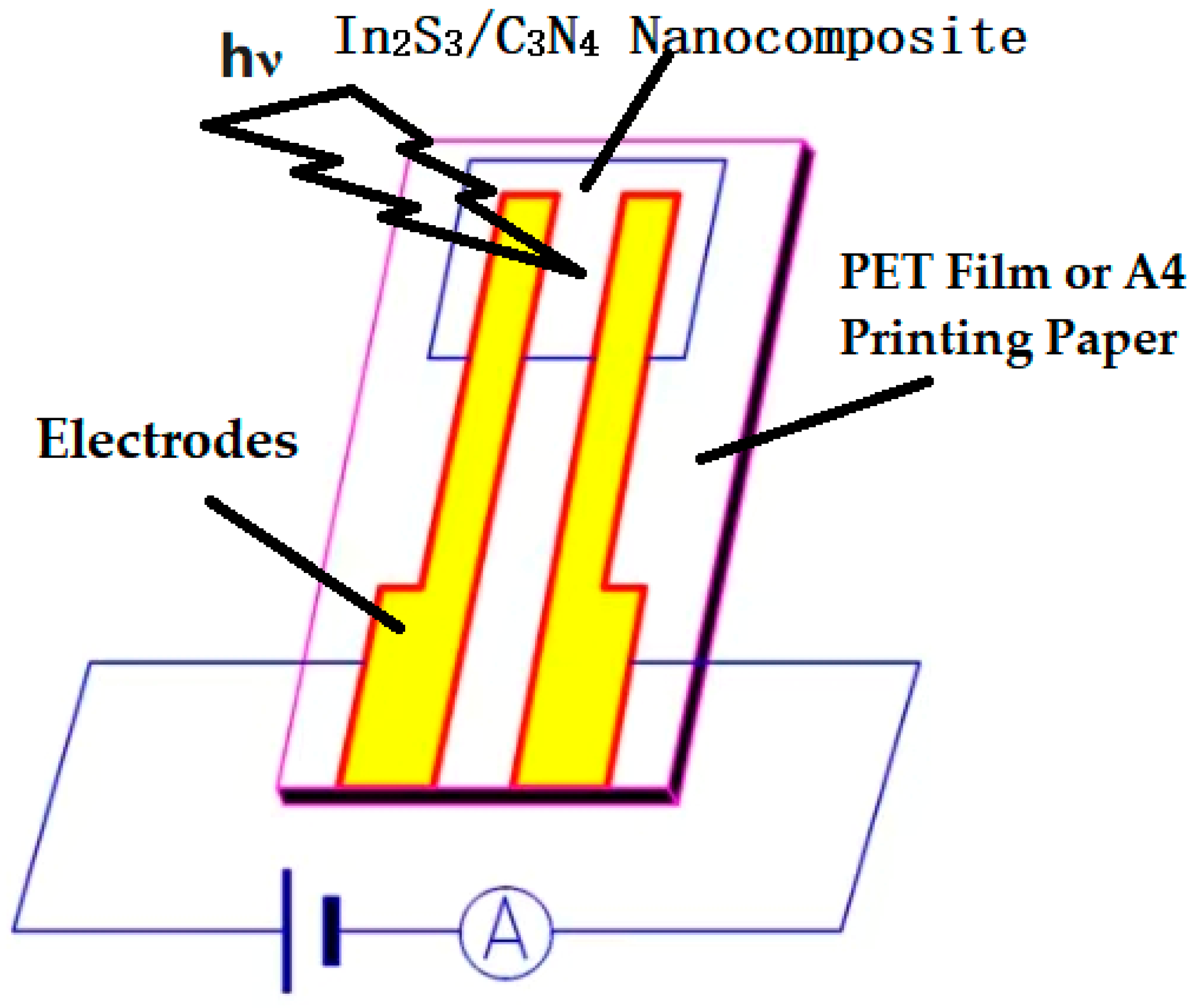
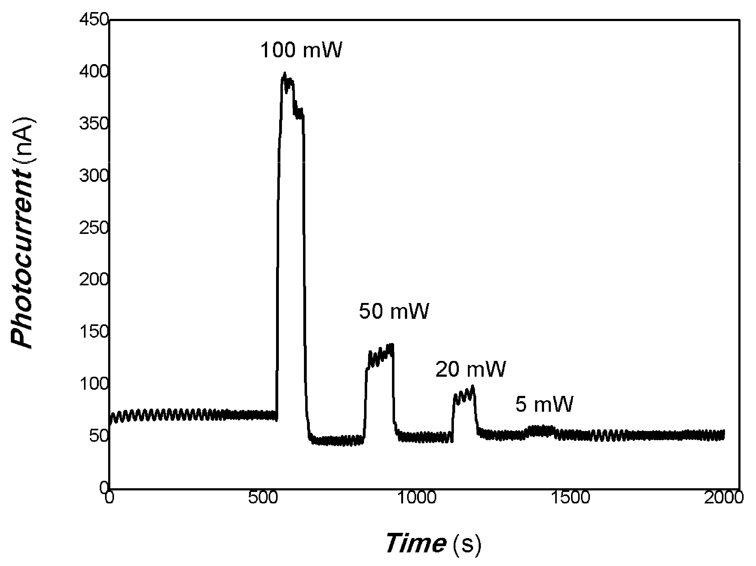
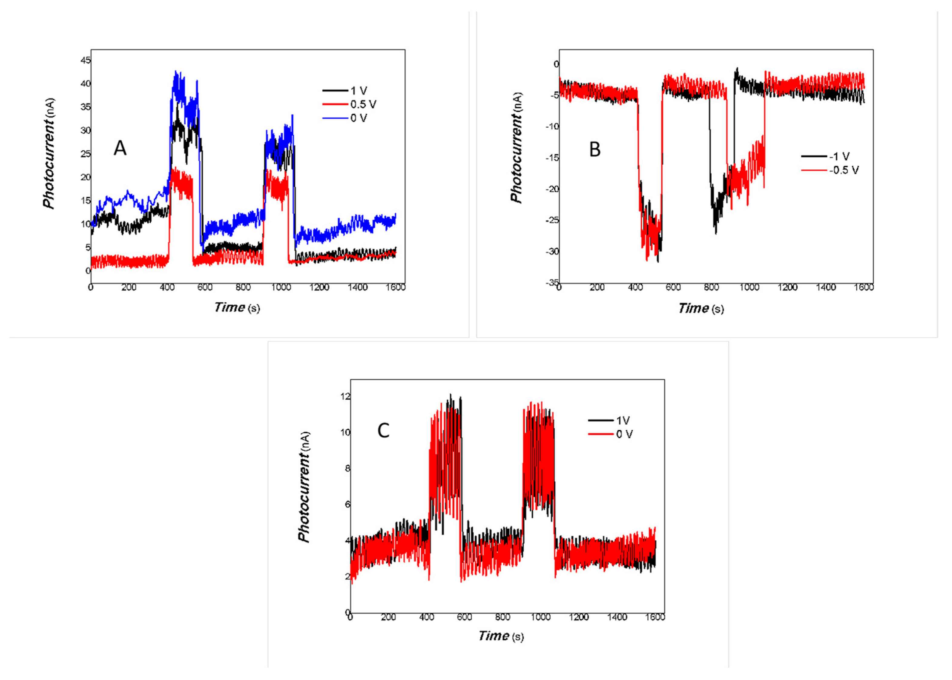
2.5. Optoelectronic Signal Determination of the In2S3/C3N4 Nanocomposite Aggregation States to the Light Sources with Different Wavelengths

The In2S3/C3N4 nanocomposite suspension was coated onto the Au gap electrodes on a flexible PET (polyethylene terephthalate) film. The commercially available gold film on PET (USA) was used in this study. The electrodes are etched using a laser. Refer to the photodetector structure of the photoconductor type, the structure of the electrodes is shown in Scheme 1. The photoconductive response to the visible light (25 W) or 405 nm, 532 nm and 650 nm (5, 10, 50 and 100 mW), and 780, 808, 980 and 1064 nm NIR (10, 50, 100 and 200 mW) was similar to the references [78]. Biases of 0, 0.5 V, 1 V, −0.5, −1 V DC were applied. The carbon electrodes with 5B pencil drawings on A4 paper were also examined due to the inexpensive cost and preparation simple.

3. Results and Discussion

It is important that the design of the nanocomposite reflects the synergy and complementarity of the different components. The band gap of In2S3 is approximately 2.3 eV, and that of C3N4 is about 2.7 eV. Both materials can only utilize part of the visible light, so does the combination of two types of partially visible light-absorbing materials extend to the near-infrared range? The key depends on the interfacial interaction between the different components and their defects. This is an important basis for the designing of functional nanocomposites with superior performance.
When preparing the In2S3/C3N4 nanocomposite, the use of sodium thiosulfate and thiourea as sulphur sources was compared. Based on the optoelectronic signals, this study focuses on the In2S3/C3N4 nanocomposite synthesised using sodium thiosulfate as sulphur source. The representative TEM and SEM image of In2S3/C3N4 nanocomposite is shown in Figure 1 and Figure 2.
Figure 1 shows that the different components have a clear morphology and are lamellar in structure. The presence of small amounts of nanoparticles is also observed. The two components are closely associated and well dispersed. This close combination is conducive to interfacial charge transfer between the different components. The size of the nanosheets was approximately 20–100 nm.
As shown in Figure 2 of the SEM, there is the presence of nanoparticles and lamellar structures. The size of the nanomaterials was approximately 20–200 nm. The results of scanning electron microscopy and transmission electron microscopy were in general agreement.
The XRD results of In2S3/C3N4 nanocomposite are shown in Figure 3. The UV-Vis-NIR of In2S3/C3N4 nanocomposite are shown in Figure 4.
As shown in Figure 3, the diffraction peaks at 28.70°, 33.44°, 47.99°, 56.78°, and 59.48° correspond to the peaks of (111), (200), (220), (311), and (222) planes of the cubic In2S3 (PDF# 05-0731), respectively. The diffraction peaks at 22.44°, 23.30°, 25.84°, 27.34°, and 28.87° correspond to the peaks of (107), (116), (204), (109), and (206) planes of the tetragonal In2S3 (PDF# 25-0390). The diffraction peak at 27.4° corresponds to the peak of (002) of C3N4 (PDF# 50-1250). Therefore, the In2S3/C3N4 nanocomposite contains In2S3 and C3N4 components.
As shown in Figure 4, it is found that although the absorption is a little weak, the absorption band edge of In2S3/C3N4 nanocomposite is still located in the NIR. It is expected that the In2S3/C3N4 nanocomposite can be used in the visible and part of the NIR. The material absorbs the photon, and the electrons jump from the ground state to the excited state, after which a series of processes, such as separation of excitons, recombination, and electron–electron or electron–phonon scattering, can occur. Defects in the material significantly impact the physical process of photoexcitation. They also determine the ratio of photogenerated carrier production, recombination, and scattering. They directly affect the transfer of photogenerated carriers. Photocurrent extraction is the result of a combination of material energy band structure, defects, interfaces, electrode materials, and its contact barrier. Further photocurrent extraction experiments will follow to confirm the absorption of the material in the visible and near infrared.
The comparative optoelectronic signal responses of In2S3/C3N4 nanocomposite aggregation states with Au electrodes on the PET film in the visible region and the NIR have been studied using different sulphur sources due to the low contact barrier of Au electrodes. The representative results are listed in Figure 5, Figure 6, Figure 7 and Figure 8.
Overall, the synthesised nanocomposites with sodium thiosulfate precursor as the sulphur source have much better optoelectronic properties than those with thiourea, which is mainly due to the defects in the resulting nanocomposites. There are differences in the defects of nanocomposites prepared using precursors with different sulphur sources, which significantly affect the extraction of their photogenerated charges. Since the defects are unavoidable in the preparation of nanocomposites, defect modulation is of great importance for the material itself. In the visible region, the optoelectrical sensitivity to the 650 nm wavelength is higher than that of the 532 and 405 nm light sources. It can be seen in Figure 5.
Figure 6 shows that the optoelectrical sensitivity of 808 nm is higher than that of 780 nm and is much bigger than that of the 980 and 1064 nm light sources. It shows that light excitation at different wavelengths reflects a certain selectivity. The In2S3/C3N4 nanocomposite aggregation states with Au electrodes on the PET film to 780, 808, 980, 1064 nm light sources exhibited good photocurrent signals. This also further supports the UV-Vis results. It can be confirmed that the UV-Vis of In2S3/C3N4 nanocomposite covered the visible region and part of the NIR. The NIR can be effectively utilised. The comparative photoelectric characteristics of In2S3/C3N4 nanocomposite aggregation states using different precursor as the sulphur source with Au electrodes on the PET film (1 V bias applied) are shown in Table 1.
As shown in Table 1, the resulting In2S3/C3N4 nanocomposite with sodium thiosulfate precursor as the sulphur source has a much higher on/off ratio and rapid response speed than that of thiourea, which is mainly due to the defect difference in the resulting nanocomposites with different precursor as the sulphur source.
As shown in Figure 5, Figure 6, Figure 7 and Figure 8, the resulting nanocomposite with thiourea as the sulphur source has a much higher baseline noise than the sodium thiosulfate precursor. Defects affect both the acquisition of optoelectronic signals and the baseline noise significantly. Noise caused by scattering is particularly noticeable. Therefore, modulating defects is an important way to improve material properties. It not only improves the acquisition of optoelectronic signals, but also significantly improves the signal-to-noise ratio and the stability of the baseline current.
The dependence of the incident light power on the photocurrent of the In2S3/C3N4 nanocomposite aggregation states with Au electrodes on the PET film using some representative light sources was examined. The results are shown in Figure 9, Figure 10 and Figure 11.
As shown in Figure 9, Figure 10 and Figure 11, the photoelectric signals are strongly dependent on the incident light power. As the power of the incident light increases, its photoelectric signal is significantly enhanced. Even when excited by 5 mW of light at 650 nm or 980 nm, the In2S3/C3N4 nanocomposite aggregation states still exhibited good photocurrent extraction. It is found that the photogenerated current is positively correlated with the power of the incident light. When the resulting nanocomposite was irradiated at a specific wavelength, the power of the incident light increased and its photogenerated current increased significantly. The dependence of the photoelectric properties of the resulting nanocomposites on the incident optical power is shown in Table 2. As acquiring photoelectric signals is the result of the energy band structure of the material, its interfaces and defects, as well as its grain boundaries, it is difficult to acquire signals for any one link that affects charge transfer. Therefore, the interfaces and grain boundaries of the resulting nanocomposite play an important role in extracting photocurrents.
The extraction of optoelectronic signals is affected by many factors of material and device structure. It is the result of the synergy of multiple interfaces. Au electrodes are widely used in various devices due to their good contact and high work function. Graphene is also widely used for flexible and transparent electrodes due to its high carrier mobility. The carbon electrodes with pencil drawings are also sometimes used in the study. The main component of the carbon electrodes with pencil drawings is graphite, other components include clay and waxes. Therefore, the conductivity of the carbon electrodes with pencil drawings is significantly lower than that of graphene, and its defects are higher than that of graphene. In many nanocomposites, it is difficult to obtain photoelectric signals with the pencil-drawn graphite electrodes. However, the cost of the graphite electrodes with pencil drawings is attractive. In this study, the In2S3/C3N4 nanocomposite with the carbon electrodes by 5B pencil drawings to several light sources from the visible region to the NIR showed good photoelectric signals. It shows that the In2S3/C3N4 nanocomposite is still easy to obtain the photocurrent signal. On the one hand, it shows that the concentration of photogenerated carriers is greater than that of defects. On the other hand, it also shows that the energy of photogenerated carriers is greater than that of defects. The contents of graphite, clay, and waxes of 5B pencil are 82%, 12%, and 5%, respectively. The pencil-drawn graphite electrodes themselves can be viewed as carbon-based composites. Their defects should not be ignored. Otherwise, the photoelectric signal was still detected, even with 0 V bias applied in this study. It is shown that the built-in electric field of the In2S3/C3N4 nanocomposite itself can facilitate the separation of photogenerated carriers. The formation of the built-in electric field is an important sign of charge transfer at the interface. The representative results are listed in Figure 12.
As shown in Figure 12, the photocurrent of the In2S3/C3N4 nanocomposite aggregation states is significantly enhanced by the 1 V bias applied. It can be seen that the bias application further accelerates the separation and transport of photogenerated charges.
The photocurrent signals of the In2S3/C3N4 nanocomposite aggregation states using other representative light sources with 0 V bias applied are shown in Figure 13 and Figure 14.
As shown in Figure 13 and Figure 14, it can be seen that although the photocurrent signal using the carbon electrodes with 5B pencil drawings on paper is not as good as that of the gold electrodes, the In2S3/C3N4 nanocomposite aggregation states can still be determined the photocurrent signals to broadband light sources with 0 V bias applied. It is suggested that the built-in electric field of the resulting nanocomposite drives charge transport and inhibits the recombination of photogenerated carriers. This field is the result of the nanocomposite’s interfacial charge transfer. Formation of the built-in electric field is also important in studying interactions between nanocomposite interfaces. Compared with Au electrodes on the PET film, the In2S3/C3N4 nanocomposite aggregation states with the carbon electrodes using 5B pencil drawings on paper have more defects of the interfaces, which limit the transport of photogenerated carriers to a great extent. These increasing defects include the carbon electrodes with 5B pencil drawings (the carbon electrodes can be considered as a composite containing graphite, clay, and waxes components), the electrode interface, and surface defects of untreated paper. These defects significantly reduce their photocurrent and lead to a very high baseline noise and stability of the photoelectric signal. Therefore, the effect of bias on the photophysical properties was investigated again using Au electrodes on the PET film and the resulting nanocomposite sample after 4 years of storage at room temperature. The results are shown in Figure 15 and Figure 16.
As shown in Figure 15 and Figure 16, at zero bias, the In2S3/C3N4 nanocomposite aggregation state with Au electrodes on the PET film still shows a better extraction of the photoelectric signal to some representative light sources. It also demonstrates a better photophysical stability of the In2S3/C3N4 nanocomposite. This is the result of a combination of materials, interfaces, defects, and grain boundaries. The photoelectric characteristics of the In2S3/C3N4 nanocomposite aggregation states with Au electrodes on the PET film are listed in Table 3 (0 V bias applied). It is significantly better than with the carbon electrodes on paper (shown in Figure 13). Figure 13 shows a large variation in the photocurrent and baseline noise. Perhaps the prototype device using the carbon electrodes with 5B pencil drawings on paper has more defects, thus increasing the chance of electron–electron and electron–phonon collisions and affecting the transport of photogenerated electrons.
The possible interfacial charge transfer between In2S3 and C3N4 nanocomposite by light excitation is shown in Scheme 2.
According to some references, the CB (conductive band) of the tetragonal In2S3 is −0.91 eV, and the VB (valance band) is 1.31 eV. The CB of the cubic In2S3 is −0.74 eV, and the VB is 1.44 eV [6]. The CB of S-doped C3N4 is −0.80 eV, and the VB is 1.48 eV [91]. The tetragonal In2S3/S-doped C3N4 is a type II heterojunction, and the cubic In2S3/S-doped C3N4 is a type I heterojunction. Type-II heterojunctions are prone to charge separation. Type I is susceptible to recombination of photogenerated carriers. Doping and defects would introduce intermediate states. This can change the type of heterojunction.
As shown in Scheme 2, the interfacial charge transfer between In2S3 and C3N4 nanocomposite is similar to that of the C, N doping effects of In2S3. C doping, N doping, or C, N co-doping are widely used to narrow the band gap of inorganic functional materials. C3N4 is a 2D conjugated polymeric material containing C, N elements. The interfacial charge transfer between In2S3 and C3N4 nanocomposite can tailor the electronic structure, optical properties, and photoelectrical properties, and result in large redshift of optical properties. In the NIR region, the In2S3/C3N4 nanocomposite aggregation states showed good photocurrent signals with the 780, 808, 980, and 1064 nm light excitation. This is mainly attributed to the introduction of defect or impurity energy levels that introduce an intermediate state. This causes a large redshift in the light excitation. It is a very significant result that the combination of two visible light-absorbing materials extends to the utilisation of near-infrared light. From the above findings, it is evident that impurities or defects have an electron-donating effect. Defect or impurity energy levels with an electron-donating effect are close to the conduction band, favouring the utilisation of near-infrared light. The non-equilibrium carrier concentration (photogenerated electrons) in the nanocomposites increases significantly under NIR photoexcitation conditions and results in positive photoconductive behaviour.
In order to investigate the effect of material composition on the photophysical properties, the EDS and EDS mapping of the In2S3/C3N4 nanocomposites were characterized. The data tables of EDS and images of EDS mapping are shown in Table 4.
In order to eliminate the interference of nuclear electric effect, the resulting nanocomposites were coated on the aluminium foil substrate during SEM and EDS sampling. As shown in Table 4, the content of the Al element is very high: the mass percentage is 91.26% and the atomic percentage is 89.81%. The aluminium element should come from the aluminium foil substrate. Aluminium foil oxidizes easily and forms a thin film of aluminium oxide on its surface. Therefore, small amounts of oxygen element (the mass percentage is 1.75% and the atomic percentage is 2.90%) also come mainly from the aluminium foil substrate. It is also possible the oxygen doping from the In2S3/C3N4 nanocomposites. Due to the hydrothermal preparation of the nanocomposite, it is possible that elemental oxygen may be present. However, it is difficult to distinguish between oxygen doping and oxygen originating from an aluminium oxide film based on the EDS results alone. When the interference of aluminium foil substrate is removed, the mass percentage of C, N, In, S elements are 5.51, 0.02, 81.31, and 13.16%, respectively. The atomic percentage of C, N, In, S elements are 29.07, 0.08, 44.85, and 26.00%, respectively. Therefore, the resulting nanocomposites are mainly In2S3 component. Based on the EDS analysis, it can be concluded that the synthesised nanocomposites are probably oxygen-doped In2S3/C3N4. Otherwise, the atomic ratio of In/S is about 1.725. It is much higher than the atomic stoichiometry ratio (0.67) of In2S3. The content of C element is quite high, and the content of N element is fairly low. The C and N elements come from the C3N4 raw material. The atomic ratio of C/N is much higher than the atomic stoichiometry ratio (0.75) of C3N4. It is likely that there are many sulphur vacancies and nitrogen vacancies. Sulphur vacancies, nitrogen vacancies, and oxygen doping play an important role in the redshift of nanomaterials. This further supports the fact that the resulting nanocomposites show good photoelectric signals in the near-infrared region. The contribution of interactions between the interfaces of different material systems to photophysical properties has also been expanded upon [92]. This reflects the authors’ sustained progress over the last 20 years in the study of the photophysical properties of nanocomposites.

4. Conclusions

In conclusion, the In2S3/C3N4 nanocomposite was constructed. This nanocomposite exhibited a photoelectric response in the visible light and near-infrared (NIR) ranges when using Au and carbon electrodes with 5B pencil drawings. It also demonstrates good photophysical stability. The photocurrent signals could still be determined when a 0 V bias is applied. This suggests that the In2S3/C3N4 nanocomposite generates a built-in field that suppresses the recombination of photogenerated charges. The presence of the built-in electric field also leads to energy band bending, which helps in the utilisation of the light with longer wavelengths. The use of different sulphur sources has a significant impact on the extraction of photogenerated carriers and baseline noise, suggesting that different sulphur sources would create different defects in the nanocomposites that could affect charge transport and baseline noise. Extraction of free charges by light excitation is the result of the synergistic action of multiple interfaces. In this study, the impurities or defects embody the electron-donating effect. Defect or impurity energy levels with an electron-donating effect are close to the conduction band, favouring the utilisation of near-infrared light. Sulphur and nitrogen vacancies, as well as oxygen doping, also play a key role in the redshift of the resulting nanocomposites. This also provides a reference for band gap modulation and the suppression of photogenerated carrier recombination. This contributes to a narrowing of the energy bands of different material systems. As defects are unavoidable during nanocomposite preparation, defect, grain boundary and property modulation will always be important for the material itself.

Author Contributions

Conceptualisation, methodology, investigation, writing—original draft preparation, writing—review and editing, funding acquisition, resources, investigation, X.M.; investigation, X.Z., M.G., R.H., and Y.W.; resources, G.L.; all authors analysed the data; all authors discussed the results of the paper. All authors have read and agreed to the published version of the manuscript.

Funding

This project was supported by the Natural Science Foundation of Shandong Province (project no. ZR2013EMM008).

Institutional Review Board Statement

This study did not involve any ethical issues.

Informed Consent Statement

Not applicable.

Data Availability Statement

The data presented in this study are available upon request from the corresponding author. The data are not publicly available due to privacy issues.

Acknowledgments

Thanks to You Wang and Guang Li of Zhejiang University for the fabrication of several electrodes and for checking the English in the paper. SEM, EDS, and EDS mapping were conducted by Jie Su, TEM was performed by Chunsheng Wang at the Structural Composition Testing Center, School of Chemistry and Chemical Engineering, Shandong University. Some students, such as Chenchen Hu took part of the experiments.

Conflicts of Interest

We declare that we have no conflicts of interest.

References

  1. Dong, C.; Chen, Q.; Deng, X.; Jiang, L.; Tan, H.; Zhou, Y.; Chen, J.; Wang, R. Enhanced Photocatalytic Hydrogen Evolution of In2S3 by Decorating In2O3 with Rich Oxygen Vacancies. Inorg. Chem. 2024, 63, 11125–11134. [Google Scholar] [CrossRef]
  2. Verma, R.; Rani, R.; Choubey, P.; Sharma, A.; Basu, M. Au Nanoparticles on In2S3/In2O3 Nanopyramids Increase Photoanodic Activity in Photoelectrochemical Water Splitting. ACS Appl. Nano Mater. 2024, 7, 26434–26444. [Google Scholar] [CrossRef]
  3. Chang, Y.; Syu, S.; Hsu, P. Construction of In2S3–In(OH)3–ZnS nanofibers for boosting photocatalytic hydrogen evolution. Int. J. Hydrogen Energy 2024, 86, 24–35. [Google Scholar] [CrossRef]
  4. Lu, P.; Du, B.; Liu, K.; Luo, Z.; Sikandaier, A.; Diao, L.; Sun, J.; Jiang, L.; Zhu, Y. Heterostructured In2O3/In2S3 hollow fibers enable efficient visible-light driven photocatalytic hydrogen production and 5-hydroxymethylfurfural oxidation. Chin. J. Struct. Chem. 2024, 43, 100361. [Google Scholar] [CrossRef]
  5. Ai, Y.; Hu, J.; Xiong, X.; Carabineiro, S.A.C.; Li, Y.; Sirotkin, N.; Agafonov, A.; Lv, K. Synergistic interfacial engineering of a S-scheme ZnO/In2S3 photocatalyst with S−O covalent bonds: A dual-functional advancement for tetracycline hydrochloride degradation and H2 evolution. Appl. Catal. B Environ. Energy 2024, 353, 124098. [Google Scholar] [CrossRef]
  6. Lin, Y.; Ko, F.; Chang, Y. Visible Light-Induced Photocatalytic Hydrogen Generation from Seawater Using Ternary Indium Sulfide/Indium Oxide/Gold Nanocomposites Obtained via Microwave-Assisted Synthesis. ACS Appl. Nano Mater. 2024, 7, 16831–16841. [Google Scholar] [CrossRef]
  7. Ye, J.; Fan, Z.; Wang, Z.; Wang, Y.; Li, J.; Xie, Y.; Ling, Y.; Chen, Y. In2S3-modified ZnIn2S4 enhanced photogenerated carrier separation efficiency and photocatalytic hydrogen evolution under visible light. Fuel 2024, 373, 132401. [Google Scholar] [CrossRef]
  8. Zhang, R.; Jia, X.; Sun, M.; Liu, X.; Wang, C.; Yu, X.; Xing, Y. Synergistic manipulation of sulfur vacancies and palladium doping of In2S3 for enhanced photocatalytic H2 production. J. Colloid Interface Sci. 2025, 677, 425–434. [Google Scholar] [CrossRef]
  9. Cruz, M.R.A.; Kim, J.H.; Torres-Martínez, L.M. Photoelectrocatalytic efficiency of In2S3–In2O3 films as photoelectrodes/photocatalyst in hydrogen production reaction. J. Phys. Chem. Solids 2024, 193, 112218. [Google Scholar] [CrossRef]
  10. Xia, Y.; Huang, G.; Fan, Y.; Zhao, X.; Wang, L.; Huang, J.; She, H.; Wang, Q. Preparation of 3D/2D ZnIn2S4/Porphyrin(Cu)-COF Type II Heterojunction: An In-Depth Insight into Interfacial Charge Transfer for Efficient Light-to-Hydrogen Conversion. J. Phys. Chem. C 2024, 128, 15000–15011. [Google Scholar] [CrossRef]
  11. Lin, Y.; Chen, L.; Zhang, J.; Gui, Y.; Liu, L. Hierarchical In2S3 microflowers decorated with WO3 quantum dots: Sculpting S-scheme heterostructure for enhanced photocatalytic H2 evolution and nitrobenzene hydrogenation. J. Mater. Sci. Technol. 2024, 174, 218–225. [Google Scholar] [CrossRef]
  12. Han, M.; Liu, L.; Guo, B.; Zhang, Z.; Li, X.; Chang, Y.; Luo, S.; Lu, W.; Li, S.; Ye, J. Bi & Mo co-doped In2S3 nano-foam blocks for boosted photocatalytic hydrogen generation. Int. J. Hydrogen Energy 2024, 78, 140–147. [Google Scholar]
  13. Li, S.; Peng, S.; Li, Y. Constructing an Open-Structured J-Type ZnIn2S4/In(OH)3 Heterojunction for Photocatalytical Hydrogen Generation. J. Phys. Chem. Lett. 2024, 15, 5215–5222. [Google Scholar] [CrossRef]
  14. Cao, J.; Xu, X.; Que, L.; Li, H.; Wang, J.; Zheng, Y.; Pan, J.; Li, C. The Cd0.8Zn0.2S/In2S3 porous nanotubes heterojunction towards enhanced visible light photocatalytic H2 evolution and photodegradation via MOFs self-template and bimetallic synergism. Renew. Energy 2024, 224, 120212. [Google Scholar] [CrossRef]
  15. Li, Y.; Yang, H.; Li, W.; Shao, Z.; Yu, Y.; Yan, H.; Jiao, S.; Lin, D.; Zhang, W.; Lv, C.; et al. P-doped ultrathin g-C3N4/In2S3 S-scheme heterojunction enhances photocatalytic hydrogen production and degradation of ofloxacin. Phys. B 2024, 685, 416053. [Google Scholar] [CrossRef]
  16. Yu, Y.; Kipkorir, A.; Choi, M.Y.; Kamat, P.V. Photocatalytic Membrane for Hydrogen Evolution: Directed Electron and Hole Transfer across Pt−AgInS2−Nafion. ACS Mater. Lett. 2024, 6, 1856–1862. [Google Scholar] [CrossRef]
  17. Wang, Z.; Wang, C.; Liu, X.; Wang, K.; Li, G. Small ZnIn2S4 Nanosheets with Abundant Edge-Active Sites Modified with MoS2 Nanosheets for Hydrogen Evolution. ACS Appl. Nano Mater. 2024, 7, 24938–24946. [Google Scholar] [CrossRef]
  18. Lin, Y.; Chang, Y.; Ko, F. One-pot microwave-assisted synthesis of In2S3/In2O3 nanosheets as highly active visible light photocatalysts for seawater splitting. Int. J. Hydrogen Energy 2024, 52, 953–963. [Google Scholar] [CrossRef]
  19. Choubey, P.; Verma, R.; Basu, M. Passivation of Surface States in CdIn2S4 via Type II Heterostructure for Boosting Photoelectrochemical Water Splitting Reaction. ACS Appl. Energy Mater. 2024, 7, 9382–9393. [Google Scholar] [CrossRef]
  20. Xiong, Y.; He, H.; Cui, Y.; Wu, Z.; Ding, S.; Zhang, J.; Peng, B.; Yang, L. Tuning Surface Electronics State of P-Doped In2.77S4/In(OH)3 toward Efficient Photoelectrochemical Water Oxidation. Langmuir 2024, 40, 8533–8541. [Google Scholar] [CrossRef]
  21. Lv, B.; Wang, Q.; He, Y.; Zhang, L.; Wang, W. In2S3 nanoparticles modify the porous Fe2V4O13 nanostructure photoanode to enhance charge separation efficiency and photoelectrochemical water splitting performance. Surf. Interfaces 2024, 49, 104469. [Google Scholar] [CrossRef]
  22. Li, J.; Liu, Z.; Li, W.; Ma, H.; Fang, P.; Xiong, R.; Pan, C.; Wei, J. In situ interfacial engineering of MnIn2S4@In2S3 hollow nanotubes for enhanced photocatalytic production of H2O2 and antibiotic degradation. J. Colloid Interface Sci. 2025, 682, 41–49. [Google Scholar] [CrossRef]
  23. Huang, S.; Gao, J.; Zhou, L.; Lei, J.; Wang, L.; Liu, Y.; Zhang, J. Polydopamine-Loaded ZnIn2S4 Photocatalyst for H2O2 Production in Water. ACS Appl. Nano Mater. 2024, 7, 4481–4490. [Google Scholar] [CrossRef]
  24. Peng, H.; Li, H.; Ye, B.; Zheng, X. Snowflake-like In2S3/Cu2S heterojunction for simultaneous photocatalytic persulfate oxidation of tetracycline hydrochloride and CO2 photoreduction. Sep. Purif. Technol. 2025, 357, 130242. [Google Scholar] [CrossRef]
  25. You, F.; Zhou, T.; Li, J.; Huang, S.; Chang, C.; Fan, X.; Zhang, H.; Ma, X.; Gao, D.; Qi, J.; et al. Rich oxygen vacancies in confined heterostructured TiO2@In2S3 hybrid for boosting solar-driven CO2 reduction. J. Colloid Interface Sci. 2024, 660, 77–86. [Google Scholar] [CrossRef]
  26. Altaf, C.T.; Colak, T.O.; Karagoz, E.; Wang, J.; Liu, Y.; Chen, Y.; Liu, M.; Unal, U.; Sankir, N.D.; Sankir, M. Co-sensitization of Copper Indium Gallium Disulfide and Indium Sulfide on Zinc Oxide Nanostructures: Effect of Morphology in Electrochemical Carbon Dioxide Reduction. ACS Omega 2024, 9, 19209–19218. [Google Scholar] [CrossRef]
  27. Gu, Z.; Chen, K.; Ding, X.; Zhang, X.; Cheng, Y.; Xiao, X.; Yu, Y. An In2O3/In2S3 photoanode-driven whole-cell biocathode sensor for sensitive detection of nitrate. Sens. Actuators B Chem. 2025, 423, 136761. [Google Scholar] [CrossRef]
  28. Wang, B.; Sun, Y.; Dong, Y.; Hou, Y.; Lu, Z.; Wei, Z.; Zhang, W.; Suematsu, K.; Hu, J. Chemiresistive flexible gas sensor for NO2 sensing at room-temperature using in situ constructed Au@In2S3/In2O3 hybrid microflowers. Sens. Actuators B Chem. 2025, 422, 136666. [Google Scholar] [CrossRef]
  29. Ou, R.; Xu, K.; Ha, N.; Ren, G.; Trinh, V.; Hu, Y.; Ma, Q.; Zhang, B.Y.; Wen, X.; Cheng, Y.; et al. Visible-Light-Driven Two-Dimensional Indium Oxysulfide for Sensitive NO2 Detection. ACS Appl. Nano Mater. 2024, 7, 14223–14231. [Google Scholar] [CrossRef]
  30. Ren, X.; Wang, M.; Chen, J.; Zhao, J.; Wang, H.; Wu, D.; Xu, R.; Zhang, Y.; Ju, H.; Wei, Q. Sulfur defect–engineered Bi2S3−x/In2S3−y mediated signal enhancement of photoelectrochemical sensor for lead ions detection. Talanta 2024, 273, 125871. [Google Scholar] [CrossRef]
  31. Li, X.; Zhang, Z.; Sun, S.; Wang, N.; Huang, B.; Li, X. Hierarchically In2S3@In2O3 nanorods heterojunctions for enhanced NO2 sensing at lower operating temperature. Sens. Actuators B Chem. 2024, 419, 136360. [Google Scholar] [CrossRef]
  32. Malathi, B.; Parveen, R.A.; Bharathi, P.; Nakamura, A.; Archana, J.; Navaneethan, M.; Harish, S. Interface engineering of 2D/2D MoS2/In2S3 heterostructure for highly sensitive NO2 detection at room temperature gas sensor. J. Environ. Chem. Eng. 2024, 12, 113023. [Google Scholar] [CrossRef]
  33. Liu, M.; Wang, Q.; Song, P. In situ synthesis of Zn-doped In2S3/In2O3 composites for the monitoring of trace ethanol at low temperature. Vacuum 2024, 222, 112956. [Google Scholar] [CrossRef]
  34. Wang, D.; Zhao, H.; Yu, H.; Chen, Y.; Ma, X.; Shang, E.; Chen, H.; Kang, X.; Zhang, J.; Tan, R.; et al. ppb-level NO2 gas sensor based on WO3/In2S3 heterostructure by hydrothermal method: A convenient and wearable real-time detection system. Ceram. Int. 2024, 50, 32678–32686. [Google Scholar] [CrossRef]
  35. Wu, Y.; Tong, Y.; Zhai, C.; Liu, Z.; Du, L.; Li, J.; Li, P.; Jiang, Y. Photocathode Biosensors Based on Au Nanoparticles and ZnIn2S4/In2S3 Composites for the Detection of Exosomal MUC1 in Breast Cancer Diagnosis. ACS Appl. Nano Mater. 2024, 7, 16758–16769. [Google Scholar] [CrossRef]
  36. Zhang, C.; Zhang, N.; Wang, X.; Gao, M.; Chen, D.; Li, Y.; Wu, Q.; Tu, J. TiO2 Nanosheet/In2S3 Nanosheet/Polydopamine Layered Composites for Constructing Enzymatic and Nonenzymatic Dual Sensors under Visible Light. ACS Appl. Nano Mater. 2024, 7, 10234–10242. [Google Scholar] [CrossRef]
  37. Zhu, F.; Zhang, S.; Zhang, Q.; Ma, K.; Wu, J.; Cai, Y. Defect-rich In2S3/CoS2 heterostructure for rapid storage of sodium ions. Electrochim. Acta 2025, 510, 145383. [Google Scholar] [CrossRef]
  38. Ahmad, M.; Inayat, A.; Hussain, M.N.; Khan, A.; Adnan; Alam, M.; Sultan, M.; Abbas, S.M. Graphene supported In2S3 nanostructure as electrode material for lithium sulfur batteries and supercapacitors. Mater. Today Sustain. 2024, 25, 100631. [Google Scholar] [CrossRef]
  39. Mishra, S.R.; Gadore, V.; Yadav, G.; Ahmaruzzaman, M. Next-generation energy storage: In2S3-based materials as high-performance electrodes for alkali-ion batteries. Next Energy 2024, 2, 100071. [Google Scholar] [CrossRef]
  40. Mishra, S.R.; Gadore, V.; Ahmaruzzaman, M. Next-generation nanotechnology: Exploring the potential of In2S3-based perovskite solar cells. Next Nanotechnol. 2024, 6, 100064. [Google Scholar] [CrossRef]
  41. Alagarasan, D.; Hegde, S.S.; Naik, R.; Murahari, P.; Shetty, H.D.; Alkallas, F.H.; Trabelsi, A.B.G.; Khan, F.S.; AlFaify, S.; Shkir, M. Fabrication of Bi-doped In2S3 thin films for highly sensitive UV photodetector applications. J. Photochem. Photobiol. A Chem. 2024, 454, 115697. [Google Scholar] [CrossRef]
  42. Jia, Z.; Li, R.; Bai, S.; Liu, Y.; Zhang, S.; Lin, Q. High-Speed and Low-Noise Photodetectors Based on Solution Processed AgInS2. ACS Photonics 2024, 11, 4349–4356. [Google Scholar] [CrossRef]
  43. Kipkorir, A.; Ealey, G.; Yu, Y.; Kamat, P.V. AgInS2-Embedded Photocatalytic Membrane: Insights into the Excited State and Electron Transfer Dynamics. Langmuir 2024, 40, 1373–1380. [Google Scholar] [CrossRef]
  44. Mishra, S.R.; Gadore, V.; Ahmaruzzaman, M. An overview of In2S3 and In2S3-based photocatalyst: Characteristics, synthesis, modifications, design strategies, and catalytic environmental application. J. Environ. Chem. Eng. 2024, 12, 113449. [Google Scholar] [CrossRef]
  45. Yu, Y.; Kipkorir, A.; Choi, M.Y.; Kamat, P.V. Directional Electron Transfer across In2S3/ZnS-Embedded Photocatalytic Membranes. ACS Appl. Energy Mater. 2024, 7, 681–688. [Google Scholar] [CrossRef]
  46. Han, S.; Zhu, Z.; Chen, F.; Sun, W.; Tang, Y. Construction of a novel multidimensional 1D/2D heterojunction FeVO4/In2S3 with significantly reinforced charge transport and excellent photocatalytic activity. J. Phys. Chem. Solids 2024, 195, 112303. [Google Scholar] [CrossRef]
  47. Chen, P.; Ou, X.; Xia, C.; Zhao, K.; Wei, M.; Wang, Y.; Zhang, M. Construction of dual Z-scheme g-C3N4/BiVO4 (040)/In2S3 photocatalyst for efficient photocatalytic degradation and sterilization under solar light irradiation. Appl. Surf. Sci. 2024, 643, 158665. [Google Scholar] [CrossRef]
  48. Dhamri, M.H.A.; Maridevaru, M.C.; Sillanpaa, M.; Kim, Y.; Selvaraj, R. Fabrication of chrysanthemums like TiO2@In2S3 S-scheme heterojunction nanostructures for the degradation of methylene blue dye present in aqueous solution. Inorg. Chem. Commun. 2024, 168, 11292. [Google Scholar]
  49. Jain, S.; Kumari, M.; Kumar, N.; Mittal, A.; Kumar, V.; Tahir, M.; Singh, P.; Rani, G.; Kataria, J.; Jogender, C. Fabrication of novel S-type In2S3/Ag2S heterostructures with superior photocatalytic and electrochemical characteristics for remediation of organic contaminants in water. Inorg. Chem. Commun. 2025, 172, 113621. [Google Scholar] [CrossRef]
  50. Tai, C.; Zhang, Z.; Ji, X.; Ma, J.; Han, X.; Wang, R.; Lu, Q.; Wei, M.; Si, C.; Chen, S.; et al. Ternary heterojunction of 1D CeO2/TiO2 nanofibers decorated with In2S3 nanosheets boosting the photodegradation of organic pollutants. Surf. Interfaces 2024, 46, 104177. [Google Scholar] [CrossRef]
  51. Liu, J.; Yuan, W.; Zhu, M.; Hu, Z.; Wu, D.; Ji, X.; Zhang, D.; Pu, X. In2S3/In2O3 Nanocomposite In Situ Forming an S-Scheme Heterojunction for the Photocatalytic Degradation of Tetracycline under Visible Light. ACS Appl. Nano Mater. 2024, 7, 20339–20348. [Google Scholar] [CrossRef]
  52. Wang, C.; Liu, N.; Liu, X.; Tian, Y.; Jiang, Q.; Chen, X.; Hou, B. Sulfur vacancy-enhanced In2S3−x hollow microtubes for photocatalytic Cr (VI) and tetracycline removal. J. Environ. Manag. 2024, 353, 120173. [Google Scholar] [CrossRef] [PubMed]
  53. Cai, M.; He, C.; Yu, H.; Shui, A. Fabrication of the ternary dual S-scheme ZnO/ZnS/In2S3 heterojunction for enhancing pollutant photodegradation. Appl. Surf. Sci. 2024, 652, 159284. [Google Scholar] [CrossRef]
  54. Wang, C.; Liu, N.; Liu, X.; Jiang, Q.; Tian, Y.; Xie, H.; Chen, X.; Hou, B. Fe doping in In2S3 hollow nanotubes for efficient photo-Fenton degradation of emerging organic pollutants. Sep. Purif. Technol. 2024, 345, 127405. [Google Scholar] [CrossRef]
  55. Su, T.; Chen, Z.; Luo, X.; Xie, X.; Qin, Z.; Ji, H. Preparation of Fe-doped In2S3/In2O3 Composite for Photocatalytic Degradation of Tetracycline. ACS Chem. Health Saf. 2024, 31, 490–502. [Google Scholar] [CrossRef]
  56. Xiao, Y.; Li, H.; Yao, B.; Wang, Y. Hollow core-shell B-g-C3N4−x@Bi2S3/In2S3 dual S-scheme heterojunction photothermal nanoreactor: Boosting photothermal catalytic activity in confined space. Chem. Eng. J. 2024, 484, 149399. [Google Scholar] [CrossRef]
  57. Wu, J.; Wang, T.; Zhang, L.; Du, P. In2S3/Cd0.9Zn0.1S Heterojunction for Efficient Photocatalytic Formic Acid Decomposition to Syngas (H2 + CO) under Visible Light. ACS Sustain. Chem. Eng. 2024, 12, 1625–1631. [Google Scholar] [CrossRef]
  58. Sharmila, B.; Divyashree, P.; Sharma, S.; Dwivedi, P.; Das, S. Scalable In2S3 based optical memristor devices as artificial synapse for logic realization and neuromorphic computing. Mater. Sci. Semicond. Process. 2025, 185, 108985. [Google Scholar]
  59. Salam, J.A.; Anand, A.M.; Raj, A.; Nath R, A.; Jayakrishnan, R. Self-powered response in β-In2S3 thin films. J. Sci. Adv. Mater. Devices 2024, 9, 100671. [Google Scholar] [CrossRef]
  60. Kharbanda, N.; Sachdeva, M.; Ghorai, N.; Kaur, A.; Kumar, V.; Ghosh, H.N. Plasmon-Induced Ultrafast Hot Hole Transfer in Nonstoichiometric CuxInyS/CdS Heteronanocrystals. J. Phys. Chem. Lett. 2024, 15, 5056–5062. [Google Scholar] [CrossRef]
  61. Guillemeney, L.; Dutta, S.; Valleix, R.; Patriarche, G.; Mahler, B.; Abécassis, B. Ligand Tail Controls the Conformation of Indium Sulfide Ultrathin Nanoribbons. J. Am. Chem. Soc. 2024, 146, 22318–22326. [Google Scholar] [CrossRef] [PubMed]
  62. Kim, K.; Havenridge, S.; Zaluzec, N.J.; Kang, D.; Jayaweera, N.P.; Elam, J.W.; Mulfort, K.L.; Liu, C.; Martinson, A.B.F. Vapor Infiltration Synthesis of Indium Sulfide Magic Size Cluster. ACS Nano 2024, 18, 31372–31380. [Google Scholar] [CrossRef] [PubMed]
  63. Amini, S.; Mohammadi, M.R.; Li, Y. Enhancing photovoltaic performance of dye-sensitized solar cells through TiO2/g-C3N4 nanocomposite photoanodes for improved charge carrier management. Electrochim. Acta 2025, 509, 145331. [Google Scholar] [CrossRef]
  64. Li, Q.; Wang, X.; Wang, W.; Wang, H.; Chen, Q.; Chen, J.; Chen, D. Constructing functionalized carbon quantum dots on amino-rich graphitic carbon nitride to enhance CO2 photocatalytic reduction: Critical role of functional group modulation. Sep. Purif. Technol. 2025, 355, 129780. [Google Scholar] [CrossRef]
  65. Guo, Z.; Li, Y.; You, Y.; Jiang, Z. Efficient UV−Vis−NIR Responsive CO2 Reduction Photocatalyst with Black Pinecone-Shaped Carbon Nitride Loaded with Lanthanum Oxide. ACS Appl. Mater. Interfaces 2024, 16, 63509–63519. [Google Scholar] [CrossRef]
  66. Zhou, F.; Li, W.; Wu, J.; Yang, W.; Sun, Y.; Zhou, H.; Jia, T.; Ling, Y.; He, P.; Pan, W.; et al. Enhanced solar-driven CO2 conversion: The role of Yb-doped CuInS2 quantum dots on g-C3N4 nanosheets. Appl. Catal. B Environ. Energy 2025, 362, 124716. [Google Scholar] [CrossRef]
  67. Yi, S.; Wang, Z.; Wu, Z.; Yang, X.; Wang, H.; Yang, J.; She, X.; Xu, H. Monodispersed Cu sites assembled on ultrathin 2D C3N4 for efficient electrocatalytic CO2 methanation. Appl. Surf. Sci. 2025, 681, 161492. [Google Scholar] [CrossRef]
  68. Zhang, B.; Liu, Y.; Wang, D.; He, W.; Fang, X.; Zhao, C.; Pan, J.; Liu, D.; Liu, S.; Chen, T.; et al. Nanoengineering construction of g-C3N4/Bi2WO6 S-scheme heterojunctions for cooperative enhanced photocatalytic CO2 reduction and pollutant degradation. Sep. Purif. Technol. 2025, 354, 128893. [Google Scholar] [CrossRef]
  69. He, Y.; Han, L.; Hou, Y.; Qiao, X.; Zhu, M. P3HT/g-C3N4 composite fiber membranes for high-performance photocatalytic hydrogen evolution. Appl. Surf. Sci. 2025, 682, 161673. [Google Scholar] [CrossRef]
  70. Yang, D.; Ye, Q.; Qu, C.; Meng, F.; Wang, L.; Li, Y. Visible-light-driven F/C co-doping g-C3N4 nanosheets for efficient hydrogen evolution: Charge redistribution on C4 delocalized large π bond. Appl. Catal. B Environ. Energy 2025, 361, 124637. [Google Scholar] [CrossRef]
  71. Lin, Y.; Wang, H.; Zhou, Y.; Wu, Y. Construction of g-C3N4-based donor-acceptor conjugated copolymer for photocatalytic selective oxidation of biomass-derived 5-hydroxymethylfurfural under visible light. J. Mol. Struct. 2025, 1322, 140404. [Google Scholar] [CrossRef]
  72. Jayaprakash, K.; Sivasamy, A. Polymeric graphitic carbon nitride layers decorated with erbium oxide and enhanced photocatalytic performance under visible light irradiation. Environ. Sci. Pollut. Res. 2023, 30, 52561–52575. [Google Scholar] [CrossRef] [PubMed]
  73. Khan, M.A.; Mutahir, S.; Shaheen, I.; Qunhui, Y.; Bououdina, M.; Humayun, M. Recent advances over the doped g-C3N4 in photocatalysis: A review. Coord. Chem. Rev. 2025, 522, 216227. [Google Scholar] [CrossRef]
  74. Nijad, I.; Pavel, G.; Roopesh, M.; Mathieu, G.; Miroslav, Š. Fine-tuning photoluminescence and photocatalysis: Exploring the effects of carbon quantum dots synthesis and purification on g-C3N4. Colloids Surf. A Physicochem. Eng. Asp. 2025, 706, 135789. [Google Scholar]
  75. Pei, J.; Li, H.; Zhuang, S.; Zhang, D.; Yu, D. Recent Advances in g-C3N4 Photocatalysts: A Review of Reaction Parameters, Structure Design and Exfoliation Methods. Catalysts 2023, 13, 1402. [Google Scholar] [CrossRef]
  76. Wang, Q.; Li, Y.; Huang, F.; Song, S.; Ai, G.; Xin, X.; Zhao, B.; Zheng, Y.; Zhang, Z. Recent Advances in g-C3N4-Based Materials and Their Application in Energy and Environmental Sustainability. Molecules 2023, 28, 432. [Google Scholar] [CrossRef]
  77. Sharma, M.D.; Basu, M. Nanosheets of In2S3/S-C3N4-Dots for Solar Water-Splitting in Saline Water. Langmuir 2022, 38, 12981–12990. [Google Scholar] [CrossRef]
  78. Ma, X.; Li, C.; Zhang, X.; Gao, M.; Wang, Y.; Li, G. Interface Optimisation of the Fe2O3/C3N4 Heterojunction with Metal Nanoparticles and Their Negative and Positive Photoelectric Responses in a Broadband Light Spectrum Range. Coatings 2024, 14, 1595. [Google Scholar] [CrossRef]
  79. Zhang, C.; Liu, K.; Ai, Q.; Sun, X.; Chen, X.; Yang, J.; Zhu, Y.; Cheng, Z.; Li, B.; Liu, L.; et al. High-performance fully transparent Ga2O3 solar-blind UV photodetector with the embedded indium–tin–oxide electrodes. Mater. Today Phys. 2023, 33, 101034. [Google Scholar] [CrossRef]
  80. Ferhati, H.; Djeffal, F.; Bendjerad, A.; Saidi, A.; Benhaya, A. Post-annealing effects on RF sputtered all-amorphous ZnO/SiC heterostructure for solar-blind highly-detective and ultralow dark-noise UV photodetector. J. Non-Cryst. Solids 2021, 574, 121168. [Google Scholar] [CrossRef]
  81. Ferhati, H.; Djeffal, F. High-Responsivity MSM Solar-Blind UV Photodetector Based on Annealed ITO/Ag/ITO Structure Using RF Sputtering. IEEE Sens. J. 2019, 19, 7942–7949. [Google Scholar] [CrossRef]
  82. Chu, L.; Xu, C.; Liu, D.; Nie, C.; Zhou, X.; Deng, L. A high-performance self-powered broadband photodetector based on vertical MAPbBr3/ZnO heterojunction. Mater. Sci. Semicond. Process. 2024, 169, 107943. [Google Scholar] [CrossRef]
  83. Lyu, Z.; Zhao, Y.; Duan, R.; Liu, M.; Yao, X.; Liu, S.; Li, S. Enhancing the performance of self-powered heterojunctional ZnO/Cs3Bi2I9 photodetectors through pyroelectric-photovoltaic coupling effect. Nano Energy 2024, 131, 110205. [Google Scholar] [CrossRef]
  84. Peng, S.; Zhang, C.; Wei, Y.; Ouyang, Y.; Han, J.; Li, C.; Dong, M.; Wang, J. High performance self-powered PbSe/WSe2 p-n heterojunction photodetector for image sensing. J. Mater. Sci. Technol. 2025, 225, 125–132. [Google Scholar] [CrossRef]
  85. Jia, M.; Tang, L.; Teng, K.S.; Lü, Y. High-performance self-powered ultraviolet photodetector based on PVK/amorphous-WO3 organic-inorganic heterojunction. Appl. Surf. Sci. 2024, 643, 158641. [Google Scholar] [CrossRef]
  86. Xiao, Y.; He, S.; Fan, X.; Du, Y.; Li, Y.; Zhao, L.; Gao, L. Realizing enhanced photoresponse for self-powered broadband photodetector with asymmetric contacts based MoTe2/WSe2 van der Waals heterostructure. J. Alloys Compd. 2024, 1006, 176358. [Google Scholar] [CrossRef]
  87. Zhang, Y.; He, X. Self-powered photodetector with GeSe/WS2/MoS2 van der Waals heterojunction. Sens. Actuators A Phys. 2025, 381, 116080. [Google Scholar] [CrossRef]
  88. Xu, W.; Li, B.; Wu, Y.; Dong, Z.; Zhang, K.; Wang, Q.; Feng, S.; Lu, W. Ultrahigh Bipolar Photoresponse in a Self-Powered Ultraviolet Photodetector Based on GaN and In/Sn-Doped Ga2O3 Nanowires pn junction. ACS Appl. Mater. Interfaces 2024, 16, 35303–35314. [Google Scholar] [CrossRef]
  89. Yang, J.; Song, J.; Zhao, X.; Zong, L.; Wang, S.; Li, B.; Li, Y.; Ban, G.; Wang, Z.; Ma, Z.; et al. Visible-Light Self-Powered Photodetector with High Sensitivity Based on the Type-II Heterostructure of CdPSe3/MoS2. ACS Appl. Mater. Interfaces 2024, 16, 32334–32343. [Google Scholar] [CrossRef]
  90. Ban, G.; Song, J.; Wang, Z.; Zhao, X.; Li, Y.; Yang, J.; Ye, C.; Teng, F.; Hu, P.; Fan, H. Visible-near-infrared self-powered photodetector based on FePSe3. Surf. Interfaces 2024, 55, 105319. [Google Scholar] [CrossRef]
  91. Pérez-Torres, A.F.; Hernández-Barreto, D.F.; Bernal, V.; Giraldo, L.; Moreno-Piraján, J.C.; da Silva, E.A.; Alves, M.D.C.M.; Morais, J.; Hernandez, Y.; Cortés, M.T.; et al. Sulfur-Doped g-C3N4 Heterojunctions for Efficient Visible Light Degradation of Methylene Blue. ACS Omega 2023, 8, 47821–47834. [Google Scholar] [CrossRef]
  92. Ma, X.; Zhang, X.; Gao, M.; Hu, R.; Wang, Y.; Li, G. The Interface Interaction of C3N4/Bi2S3 Promoted the Separation of Excitons and the Extraction of Free Photogenerated Carriers in the Broadband Light Spectrum Range. Inorganics 2025, 13, 122. [Google Scholar] [CrossRef]
Scheme 1. The structure of the Au or carbon electrodes.
Coatings 15 00718 sch001
Figure 1. The representative TEM image of In2S3/C3N4 nanocomposite (the scale bar: left is 200 nm; Right is 100 nm).
Coatings 15 00718 g001
Figure 2. The SEM images of In2S3/C3N4 nanocomposite (the scale bar: left is 300 nm; right is 1 μm).
Coatings 15 00718 g002
Figure 3. The XRD results of In2S3/C3N4 nanocomposite.
Coatings 15 00718 g003
Figure 4. The UV-Vis-NIR of In2S3/C3N4 nanocomposites ((A) using sodium thiosulfate precursor as a sulphur source; (B) using thiourea precursor as a sulphur source).
Coatings 15 00718 g004
Figure 5. The comparative results of In2S3/C3N4 nanocomposite aggregation states with Au electrodes on the PET film to 50 mW 405, 532, 650 nm light sources ((A) using sodium thiosulfate precursor as a sulphur source; (B) using thiourea precursor as a sulphur source) (with 1 V bias).
Coatings 15 00718 g005
Figure 6. The comparative results of In2S3/C3N4 nanocomposite aggregation states with Au electrodes on the PET film to 50 mW 780, 808, 980 nm and 40 mW 1064 nm light sources ((A) using sodium thiosulfate precursor as a sulphur source; (B) using thiourea precursor as a sulphur source) (1 V bias).
Coatings 15 00718 g006
Figure 7. The comparative results of In2S3/C3N4 nanocomposite aggregation states with Au electrodes on the PET film to 50 mW 808 nm light sources ((A) using sodium thiosulfate precursor as a sulphur source; (B) using thiourea precursor as a sulphur source) (1 V bias).
Coatings 15 00718 g007
Figure 8. The comparative results of the In2S3/C3N4 nanocomposite aggregation states with Au electrodes on the PET film to 25 W visible light sources ((A) using sodium thiosulfate precursor as a sulphur source; (B) using thiourea precursor as a sulphur source) (with 1 V bias).
Coatings 15 00718 g008
Figure 9. The comparative results of In2S3/C3N4 nanocomposite aggregation states using Au electrodes on the PET film to 650 nm light sources with different power (using sodium thiosulfate precursor as a sulphur source) (with 1 V bias).
Coatings 15 00718 g009
Figure 10. The comparative results of In2S3/C3N4 nanocomposite aggregation states using Au electrodes on the PET film to 808 nm light sources with different power (using sodium thiosulfate precursor as a sulphur source) (1 V bias).
Coatings 15 00718 g010
Figure 11. The comparative results of In2S3/C3N4 nanocomposite aggregation states using Au electrodes on the PET film to 980 nm light sources with different power (using sodium thiosulfate precursor as a sulphur source) (1 V bias).
Coatings 15 00718 g011
Figure 12. The comparative results of the In2S3/C3N4 heterojunction aggregation states using the carbon electrodes with 5B pencil drawings on paper to 100 mW 980 nm light sources (0, 1 V bias, respectively).
Coatings 15 00718 g012
Figure 13. The comparative results of the In2S3/C3N4 nanocomposite aggregation states using the carbon electrodes with 5B pencil drawings on paper as substrate to 50 mW 405, 532, 650, 780 nm light sources ((A) 405 nm; (B) 532 nm; (C) 650 nm; (D) 780 nm) (with 0 V bias).
Coatings 15 00718 g013
Figure 14. The comparative results of the In2S3/C3N4 nanocomposite aggregation states using the carbon electrodes with 5B pencil drawings on paper to 808, 980, and 1064 nm light sources ((A) 200 mW 808 nm; (B) 100 mW 980 nm; (C) 20 mW 1064 nm) (with 0 V bias).
Coatings 15 00718 g014
Figure 15. The comparative results of In2S3/C3N4 nanocomposite aggregation state with Au electrodes on the PET film to (A) 200 mW 808 nm (0, 0.5, 1 V bias); (B) 200 mW 808 nm (−0.5, −1 V bias); (C) 100 mW 980 nm (0, 1 V bias).
Coatings 15 00718 g015
Figure 16. The comparative results of In2S3/C3N4 nanocomposite aggregation state with Au electrodes on the PET film to some representative light sources ((A) 50 mW 405; (B) 50 mW 532 nm; (C) 50 mW 650 nm; (D) 50 mW 780 nm light sources) (using 0 V bias).
Coatings 15 00718 g016
Scheme 2. The possible interfacial charge transfer between In2S3 and C3N4 nanocomposite by light excitation.
Coatings 15 00718 sch002
Table 1. The comparative photoelectric characteristics of In2S3/C3N4 nanocomposite aggregation states using different precursor as the sulphur source with Au electrodes on the PET film (1 V bias).
Excitation Light
Wavelength (nm)
In2S3/C3N4 NanocompositeResponse Time
(s)
Recovery Time
(s)
Ratio of On/Off
50 mW 405 nmusing sodium thiosulfate precursor as a sulphur source19.712.02.14
50 mW 405 nmusing thiourea precursor as a sulphur source12.020.61.23
50 mW 532 nmusing sodium thiosulfate precursor as a sulphur source32.616.32.14
50 mW 532 nmusing thiourea precursor as a sulphur source56.64.31.23
50 mW 650 nmusing sodium thiosulfate precursor as a sulphur source24.012.02.43
50 mW 650 nmusing thiourea precursor as a sulphur source36.816.31.24
50 mW 780 nmusing sodium thiosulfate precursor as a sulphur source7.712.01.74
50 mW 780 nmusing thiourea precursor as a sulphur source12.029.11.27
50 mW 808 nmusing sodium thiosulfate precursor as a sulphur source12.016.31.85
50 mW 808 nmusing thiourea precursor as a sulphur source8.612.01.40
50 mW 980 nmusing sodium thiosulfate precursor as a sulphur source4.312.01.26
50 mW 980 nmusing thiourea precursor as a sulphur source8.68.61.32
40 mW 1064 nmusing sodium thiosulfate precursor as a sulphur source8.67.71.24
40 mW 1064 nmusing thiourea precursor as a sulphur source4.328.31.16
25 W, visible lightusing sodium thiosulfate precursor as a sulphur source20.620.53.00
25 W, visible lightusing thiourea precursor as a sulphur source12.016.31.77
Table 2. The photoelectric characteristics of the In2S3/C3N4 nanocomposite aggregation states with Au electrodes on the PET film (using sodium thiosulfate precursor as a sulphur source) to some representative light sources (with 1 V bias).
Excitation Light
Wavelength (nm)
Response Time (s)Recovery Time (s)Ratio of On/Off
100 mW, 650 nm12.016.35.67
50 mW, 650 nm5.74.32.86
5 mW, 650 nm15.615.11.15
100 mW, 808 nm16.38.12.11
50 mW, 808 nm20.68.11.96
10 mW, 808 nm8.18.11.24
100 mW, 980 nm16.37.72.03
50 mW, 980 nm8.68.61.33
5 mW, 980 nm8.64.31.05
Table 3. The photoelectric characteristics of the In2S3/C3N4 nanocomposite aggregation states with Au electrodes on the PET film to some representative light sources (using sodium thiosulfate precursor as a sulphur source) (using 0 V bias).
Excitation Light
Wavelength (nm)
Response Time (s)Recovery Time (s)Ratio of On/Off
50 mW, 405 nm6.616.61.79
50 mW, 532 nm16.56.51.80
50 mW, 650 nm3.43.13.40
50 mW, 780 nm16.23.13.41
200 mW, 808 nm22.86.62.66
100 mW, 980 nm9.710.03.17
Table 4. The comparative results of EDS and EDS mapping of In2S3/C3N4 nanocomposites.
Nanocomposite SampleC Element (Mass Percentage (%))N Element (Mass Percentage (%))In Element (Mass Percentage (%)) S Element (Mass Percentage (%))Total (%)
In2S3/C3N4 coated on aluminum foil2.470.003.201.33100.00 (Otherwise, Al element mass percentage: 91.26%; O element mass percentage: 1.75%)
C element (atomic percentage (%))N element (atomic percentage (%))In element (atomic percentage (%))S element (atomic percentage (%))Total (%)
In2S3/C3N4 coated on aluminum foil5.450.000.741.10100.00 (Otherwise, Al element atomic percentage: 89.81%; O element atomic percentage: 2.90%)
C element (mass percentage (%))N element (mass percentage (%))In element (mass percentage (%))S element (mass percentage (%))Total (%)
In2S3/C3N4 (remove the effects of aluminum foil)5.510.0281.3113.16100.00
C element (mass percentage (%))N element (mass percentage (%))In element (mass percentage (%))S element (mass percentage (%))Total (%)
In2S3/C3N4 (remove the effects of aluminum foil)29.070.0844.8526.00100.00
Coatings 15 00718 i001
Coatings 15 00718 i002
Disclaimer/Publisher’s Note: The statements, opinions and data contained in all publications are solely those of the individual author(s) and contributor(s) and not of MDPI and/or the editor(s). MDPI and/or the editor(s) disclaim responsibility for any injury to people or property resulting from any ideas, methods, instructions or products referred to in the content.

