Article

Effect of Gas Velocity on Thickness Uniformity of TiNxOy Thin Film in Atomic Layer Deposition Process

Division of Semiconductor Engineering, Myongji University, Yongin-si 17058, Republic of Korea
*
Author to whom correspondence should be addressed.
Coatings 2025, 15(6), 707; https://doi.org/10.3390/coatings15060707
Submission received: 27 April 2025 / Revised: 3 June 2025 / Accepted: 9 June 2025 / Published: 12 June 2025
(This article belongs to the Special Issue Semiconductor Thin Films and Coatings)

Abstract

Atomic layer deposition (ALD) has emerged as an essential technique, enabling the deposition of titanium nitride (TiN), which is renowned for its exceptional metal diffusion barrier properties. Improving within-wafer uniformity has become increasingly important to actively transition from lab-scale process development to wafer manufacturing. We considered the effect of gas velocity on thickness uniformity through computational fluid dynamics (CFD) simulations. Gas velocity was controlled by varying equipment design parameters, and it was confirmed that the resulting reduction in velocity improved both velocity and thickness uniformity. To validate the simulation results, an ALD reactor was experimentally performed under the same design and process conditions. The measured thickness of the deposited films confirmed an improvement in thickness uniformity, and the cause of the thickness reduction was further investigated. This study demonstrates that controlling gas velocity prov ides valuable insights into improving thickness uniformity in the ALD reactor. It confirms the effectiveness of simulations in overcoming the limitations associated with considering various process and equipment variables, which can be time-consuming and costly. Furthermore, it emphasizes the importance of integrating flow dynamic simulations with process evaluations to contribute to the advancement of semiconductor manufacturing technologies.

Graphical Abstract

1. Introduction

The continuous scaling down of semiconductor components and devices is driving the development of advanced fabrication technologies [1,2,3,4,5]. To create nanoscale semiconductor devices, more precise processing methods are required [6,7,8]. Atomic layer deposition (ALD) has been introduced as a processing technique capable of precisely controlling the deposited film’s thickness at the atomic level. ALD exhibits characteristics of self-limiting reactions, allowing for the deposition of only one layer of thin film at a time. This enables deposition at the atomic layer level, characterized by excellent step coverage and uniformity [9,10,11,12,13,14,15]. In semiconductor processing, one of the materials predominantly deposited via ALD is titanium nitride (TiN). While it was previously deposited through physical vapor deposition (PVD), the demand for superior step coverage due to the downscaled components has led to its primary deposition via ALD [16,17,18].
ALD-deposited thin films are generally known for their excellent uniformity; however, several factors can degrade this uniformity during the deposition process. These factors include the following: 1) overlapping material pulses, 2) non-uniform gas distribution or non-uniform precursor distribution in the carrier gas, and 3) thermal self-decomposition of the precursor. In addition, various factors affecting uniformity have been studied, including the effect of gaseous by-products on ALD growth [19]. Uniformity is a critical parameter directly associated with not only manufacturability but also the performance and reliability of semiconductor devices. Consequently, we became interested in thickness uniformity and factors affecting thickness uniformity.
Simulations have been extensively employed in research to enhance ALD reactors by enabling a comprehensive understanding and detailed analysis of the various factors impacting performance [20,21,22,23,24,25]. Yichi Zhang et al. developed a multiscale computational fluid dynamics (CFD) model for the thermal ALD of SiO2, achieving a 39.6% reduction in half-cycle time through reactor geometry optimization [20]. Kim et al. [24] performed a comparative study of aluminum precursors in area-selective atomic layer deposition (AS-ALD) using density functional theory (DFT), examining the potential energy profiles of trimethylaluminum (TMA) and dimethylaluminum isopropoxide (DMAI) to determine the origin of deposition selectivity differences. By integrating multiple variables into computational models, simulations enable a more comprehensive analysis of ALD reactors, thereby facilitating a deeper understanding of process characteristics. Accordingly, we aimed to analyze the flow behavior and thickness uniformity within the ALD chamber during process operation, aspects that are difficult to observe experimentally.
This study investigates the influence of gas flow velocity on the thickness uniformity of thin films. Gas velocity is a critical parameter that significantly affects thin films, as it is closely related to the adsorption and desorption times of precursors and reactants on the substrate’s surface. However, due to the typical high-temperature and low-pressure conditions of semiconductor processes, controlling and analyzing gas velocity present substantial challenges. While previous studies have explored the relationship between gas velocity and growth rate, research on its impact on thickness uniformity remains limited [26].
To address this, gas flow and velocity distributions within a high-temperature, low-pressure chamber were analyzed using CFD. Gas velocity was varied by applying models with different inlet diameters, and the resulting changes in chamber flow velocity, gas density, speed distribution, and thickness uniformity were investigated. Based on these analyses, the mechanisms by which gas velocity affects thickness uniformity were examined. To validate the simulation results, thin films were deposited under identical design and process conditions. The subsequent analysis compared the simulation and experimental results with a primary focus on thickness uniformity, rather than the functional properties of the films themselves.

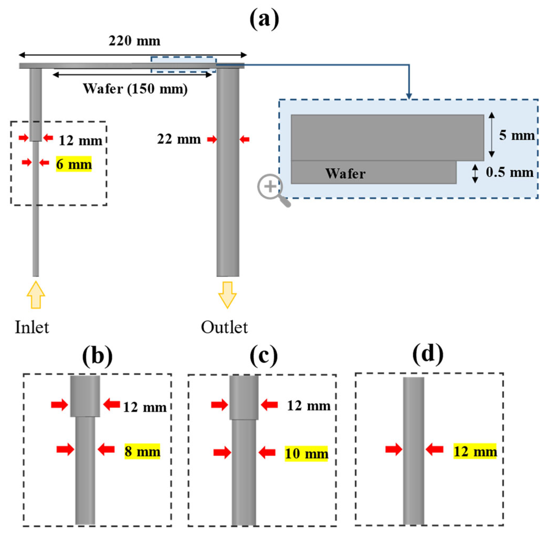
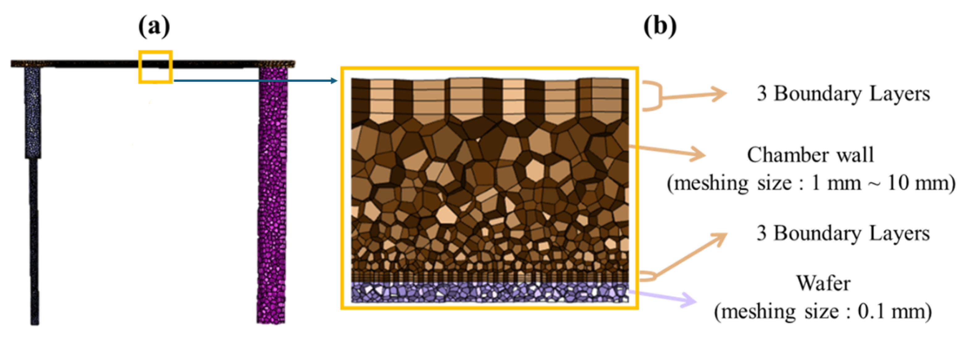
2. Simulation Methods

In this study, computational fluid dynamics (CFD) simulations were conducted for analysis. The structure of the thermal ALD equipment consists of one inlet with a diameter of 12 mm and one outlet with a diameter of 22 mm, without a separate showerhead. The geometry was created using Ansys SpaceClaim (3D modeling software), as illustrated in Figure 1. To adjust the inlet injection velocity, models were created by increasing the diameter of the existing gas line from 6 to 12 mm in 2 mm increments, and the detailed dimensions, including these modifications, are presented in Figure 2. To evaluate the orthogonality of the generated mesh, the orthogonal quality metric is used. Rather than the average value, the minimum orthogonal quality is typically considered to identify the worst-case cell shape in the mesh. In this study, the minimum orthogonal quality was set to 0.2, as shown in Figure 3. Specifically, since the depth of the chuck where the wafer was placed was very small (0.5 mm), meshing was conducted with an even smaller size of 0.1 mm, as shown in Figure 3b. To accurately capture the effects of wall viscosity, a three-layer boundary layer was defined near the wall to enhance calculation accuracy. ANSYS Fluent, 2024 R1, was utilized for CFD analysis. In the TiN deposition process, tetrakis (dimethylamido)-titanium (TDMAT), provided by Moman, Co., Ltd., Ansan-si, Republic of Korea, was used as the precursor, ammonia (NH3) as the reactant, and argon (Ar) as the purge gas.
For chemical reactions, wall surface reactions were included to model the deposition of TiN on the wafer, while volumetric reactions were implemented to simulate the purging process with Ar. The wall surface reactions for TiN deposition are defined as presented in Table 1 [27]. The surface reactions are simplified into two processes: Reaction 1, where the precursor is adsorbed, and Reaction 2, where the reactant gas is adsorbed. The Arrhenius constants required for the surface reactions were referenced from published studies, with bulk values applied accordingly [28]. For boundary conditions, the inlet condition was specified by mass flow rate, while the outlet condition was specified by pressure, as shown in Table 2. Process gases were injected with profiles arranged as follows: TDMAT for 11 s – Ar for 45 s – NH3 for 5 s – Ar for 35 s. The chuck temperature was set at 523 K. The profile and boundary conditions were established based on the saturation conditions determined in previous research, and the experimental conditions were configured accordingly [29]. To match the experimental conditions, the mass flow rates of each gas were obtained by converting the volumetric flow rates using their densities, as shown in Equation (1). Since no reliable data on the temperature-dependent vapor density and volumetric flow rate of TDMAT were available in the literature or product datasheets, approximate values were used as practical inputs for the simulation. The volumetric flow rate of TDMAT was estimated to be approximately 19.73 sccm, based on the experimentally observed injection pressure of 0.25 torr. This value was calculated using the standard conversion factor of 1 torr = 78.93 sccm (air equivalent) by multiplying the factor by 0.25. For the vapor density, a representative value of 7.5, corresponding to the relative vapor density at 20 °C, was adopted. These approximations are considered reasonable for reactor-scale flow modeling purposes [30].
m i ˙ = V i ˙ × ρ i 60 × 10 6
where i denotes the type of gas, and V represents the volumetric flow rate. The mass flow rate is calculated by multiplying the volumetric flow rate (V) by the gas density ( ρ ) and dividing by 60 × 106 to convert the unit from cm3/min to m3/s.

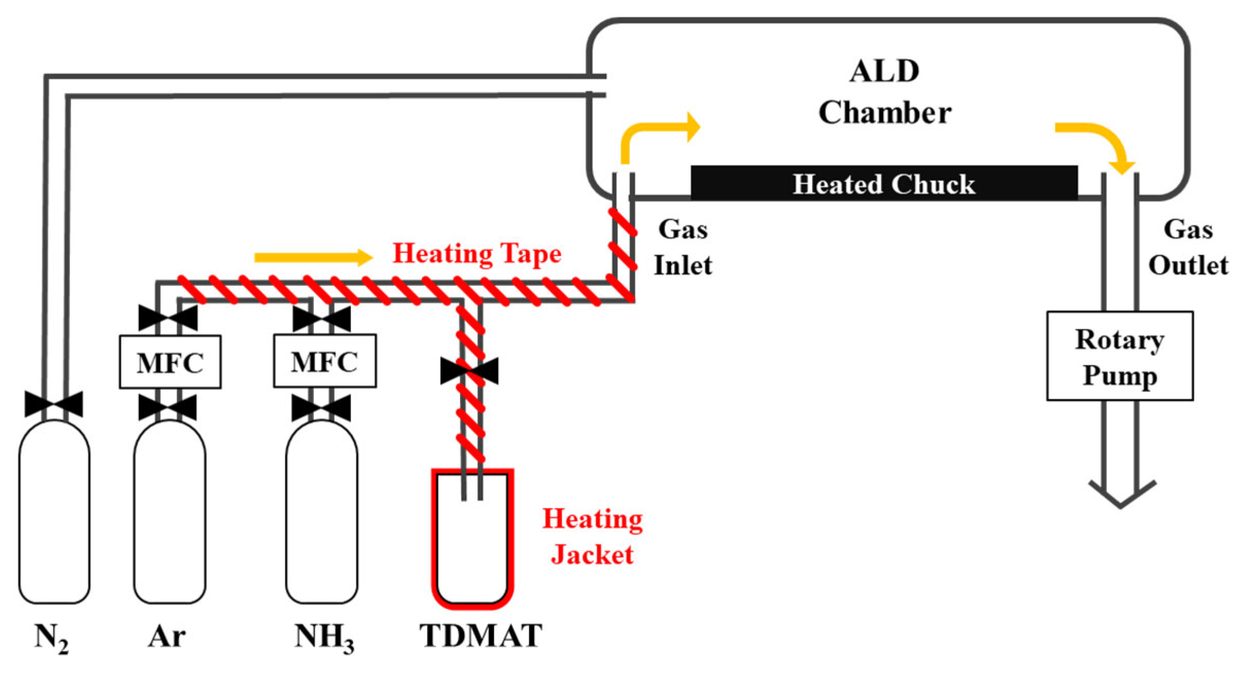
3. Experimental Method

We used a 6-inch R&D ALD system (Model IC-10, Moman, Republic of Korea) located in the Semiconductor Process Diagnosis Research Center (SPDRC) at Myongji University to deposit the TiN-ALD film, as illustrated in Figure 4. The conventional 6 mm gas line was configured with its upper end connected to the chamber inlet and its lower end connected to the TDMAT precursor. For the experiment, the gas line connected to the inlet was replaced with a newly fabricated 12 mm line while maintaining the inlet diameter unchanged, as shown in Figure 5. In this study, 150 mm diameter p-type boron-doped silicon wafers were used, with a crystal orientation of (100) ± 0.5°, a resistivity of 1–10 Ω·cm, and a thickness of 525 ± 25 μm. The wafers were prime grade, single-side polished, and equipped with extended flats. The polished surface exhibited atomic-level flatness (Ra < 0.5 nm), making the wafers highly suitable for ALD reactors where thin film uniformity and clean interfaces are critical. The film was deposited on the wafer at 250 °C, utilizing TDMAT as the precursor, known for its excellent corrosion resistance [31]. NH3 and Ar were used as reactant gas and purge gas, respectively. The flow rates of each process gas were determined based on the saturation conditions used in previous studies, consistent with the simulation conditions. Each cycle of the ALD reactor consisted of TDMAT for 11 s, Ar at 50 sccm for 45 s, NH3 at 50 sccm for 5 s, and Ar at 50 sccm for 35 s. The heating jacket temperature of TDMAT was set to 36 °C, and the heating tape for the gas line was maintained at 80 °C. The thickness of the film was measured using ellipsometry (Elli-SEU-am12, Ellipso Technology, Suwon, Republic of Korea). A single-layer Lorentz-12 model was applied for data interpretation, considering a three-layer structure composed of ambient air, a TiN thin film, and a silicon substrate (C-Si-UVI). The film was treated as a single optical layer in the analysis. Although the film deposited through the actual process was closer to TiNxOy rather than a pure TiN single film, previous studies have reported that such oxynitride films exhibit similar refractive index (n) and extinction coefficient (k) values to those of stoichiometric TiN. Therefore, the use of a TiN-based dispersion model was considered to be a reasonable approximation [32]. To verify the model’s accuracy, fitting error sigma values were obtained from 49 measurement points per sample. The calculated average sigma values were 0.00677 for the 6 mm gas line diameter and 0.00730 for the 12 mm gas line diameter, with small standard deviations of 0.00020 and 0.00018, respectively. The film composition and crystal structure were analyzed by X-ray photoelectron spectroscopy (KRATOS ULTRA2, Manchester, UK) and X-ray diffraction (Bruker, Billerica, MA, USA), respectively.

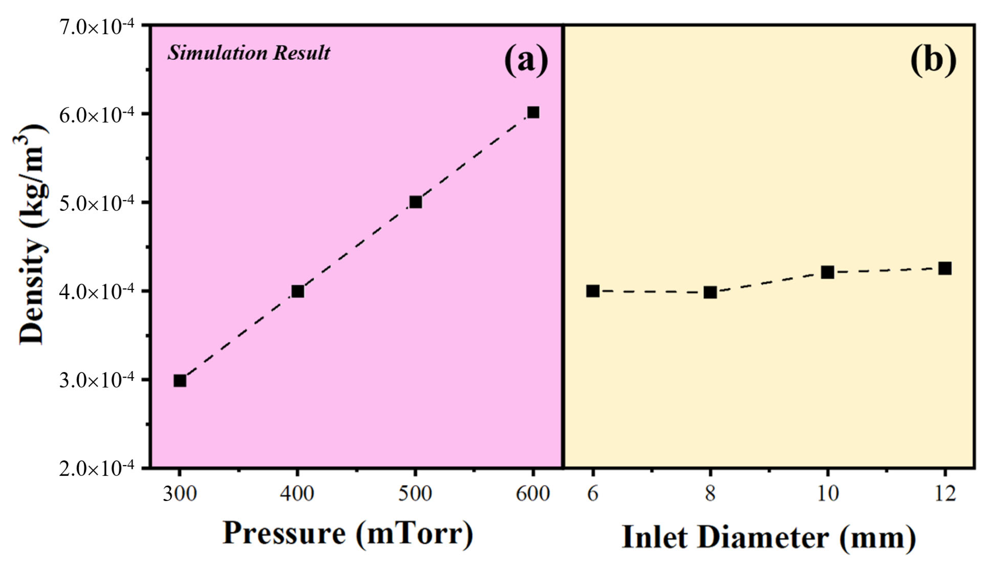
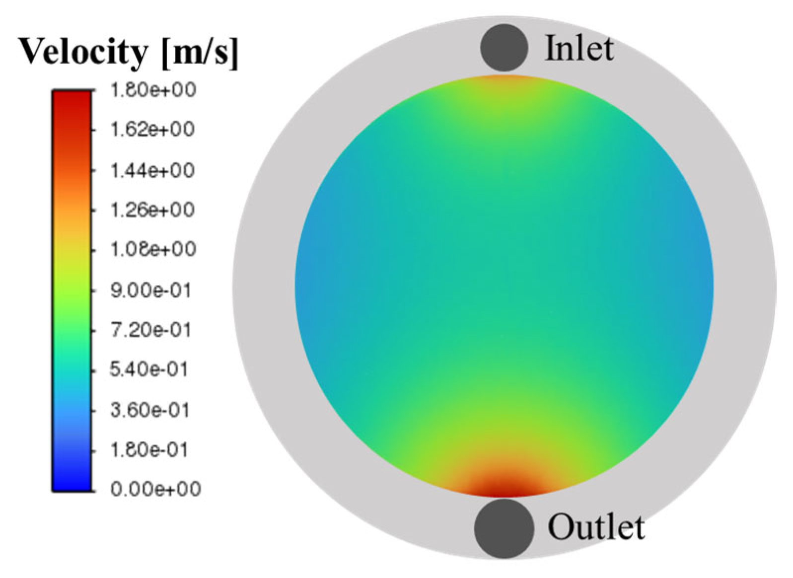
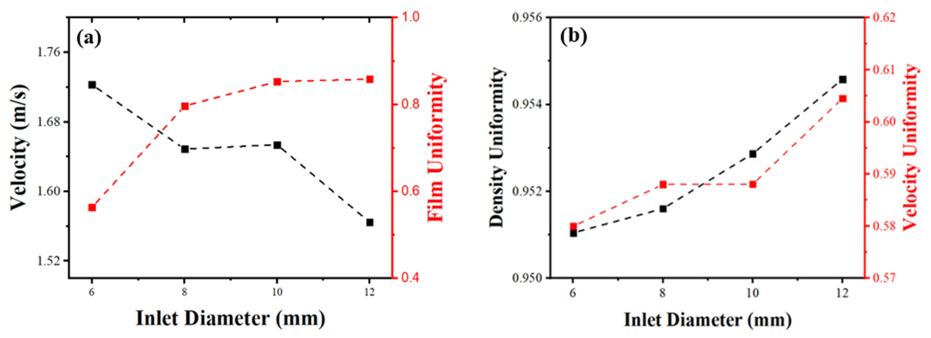
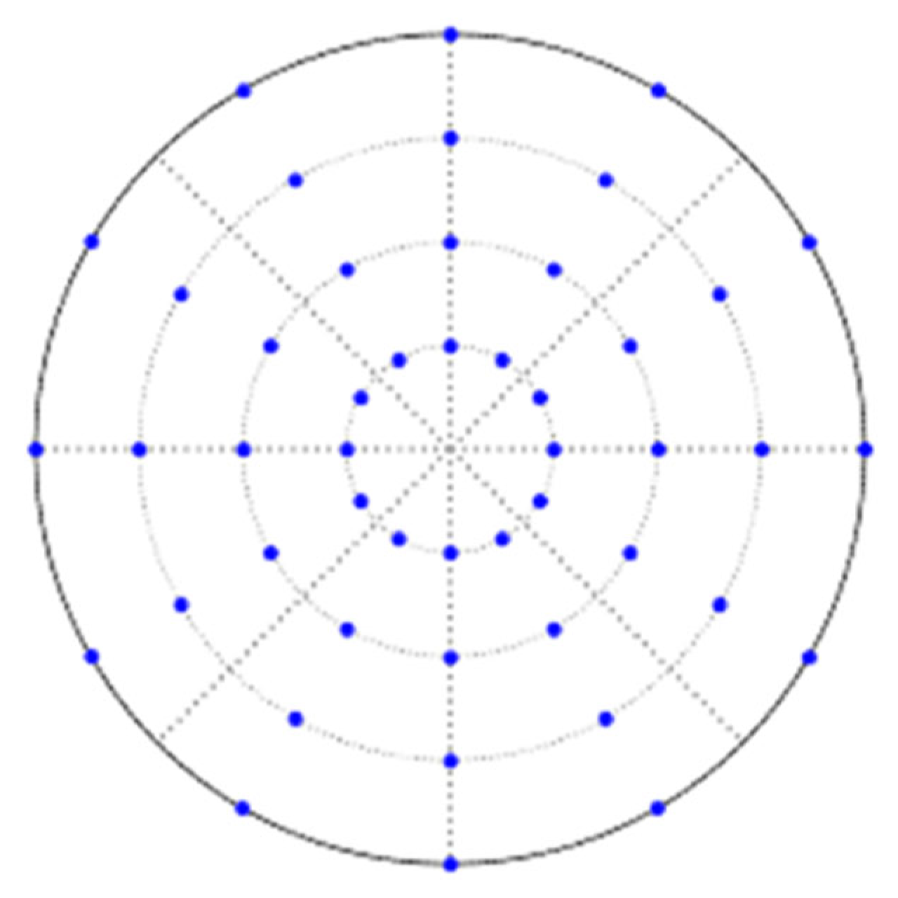
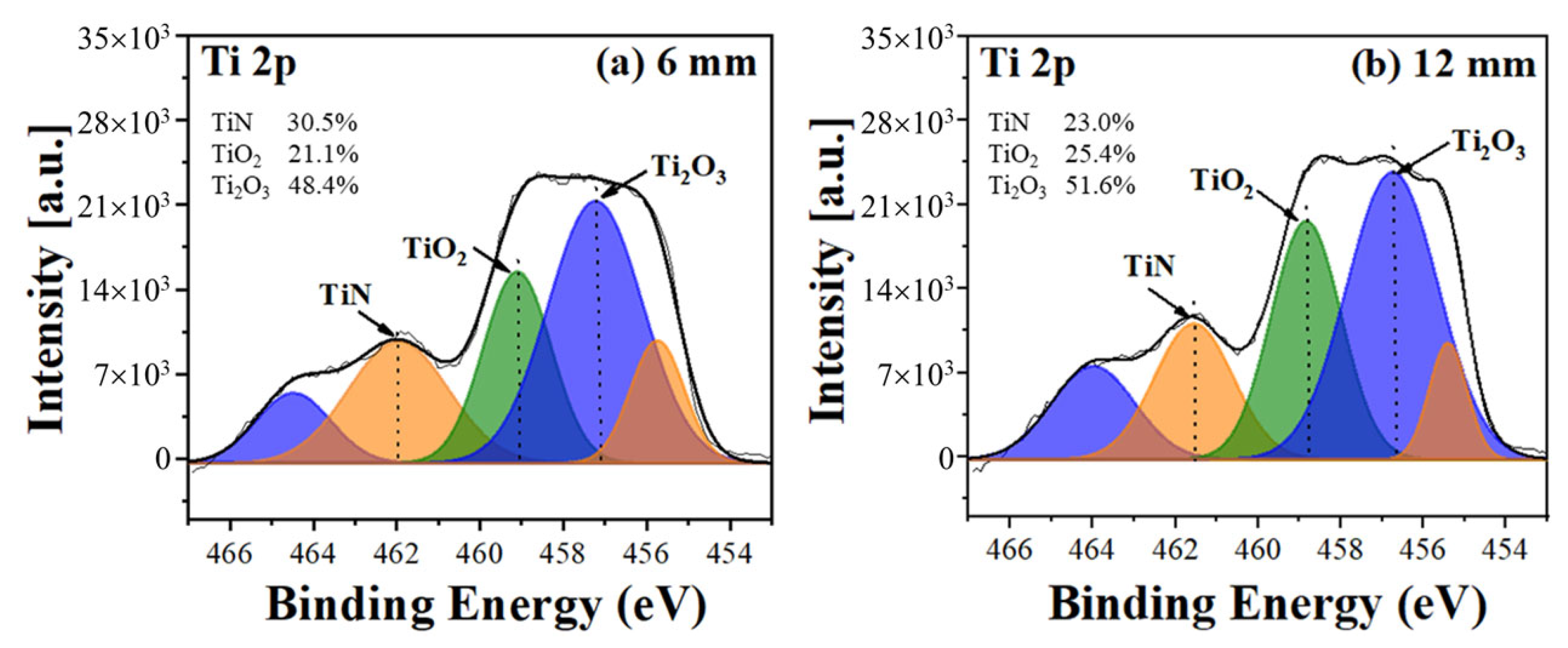
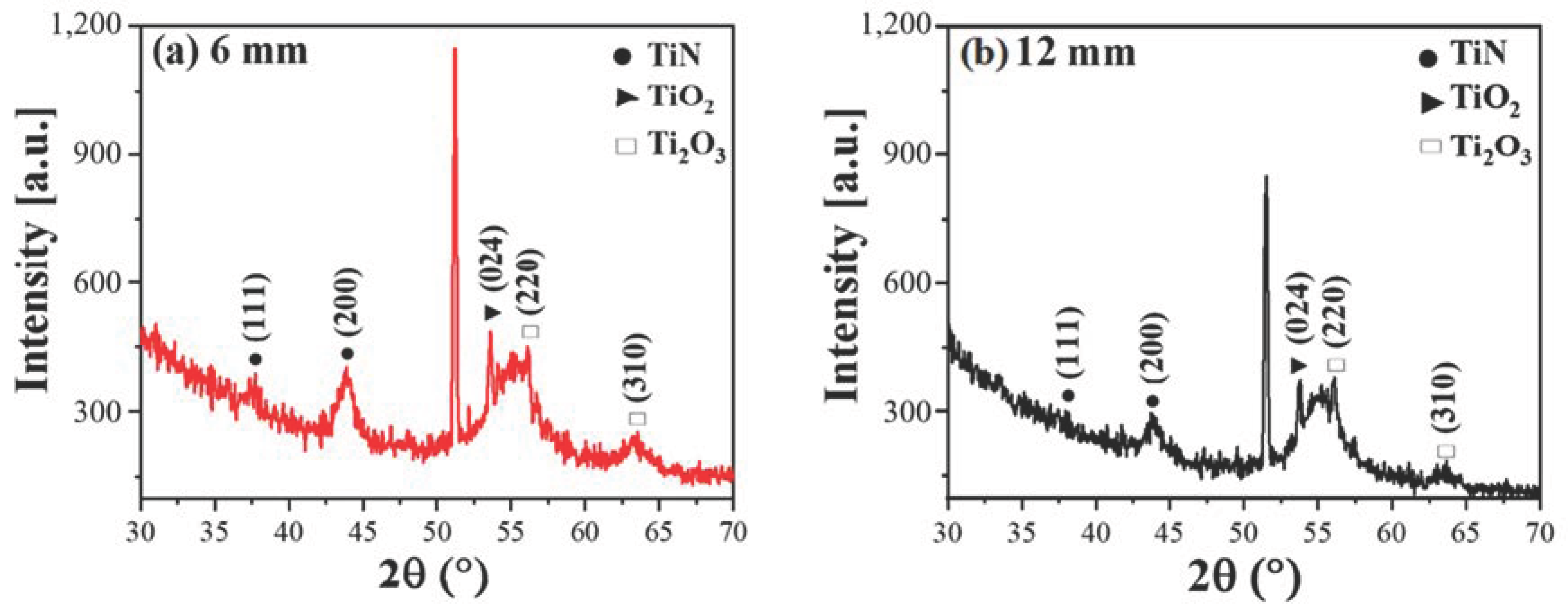
4. Results and Discussion

We determined the gas inlet diameter of our thermal ALD equipment as a design variable, as shown in Figure 2. The inlet diameter varied from 6 to 12 mm in 2 mm increments, while the pressure was set to 400 mTorr. The simulation results for parameters such as density and velocity were analyzed based on the state at 96 s, at which point all gases had been fully introduced. The representative average values for each parameter and the uniformity were calculated using the following equations:
a ¯ = i = 1 n i A i i = 1 n A i
γ a = 1 i = 1 n [ ( i a ¯ ) A i ]   2 a ¯ i = 1 n A i
where i is the facet index of a surface composed of multiple facets, and a denotes “area-weighted”. ∅ represents the average value of the field variable on the surface. The area-weighted average ( a ¯ ) was calculated by weighing the average value of each facet by its area to account for the different cross-sectional areas of the cells generated through meshing. The uniformity, calculated using Equation (3), was derived from the difference between the area-weighted average, in Equation (2), and the corresponding facet index value.
In the early stage of this study, pressure was selected as a variable to control the gas velocity. However, as shown in Figure 6a, adjusting velocity via pressure resulted in a sharp increase in gas density. Therefore, the inlet diameter was used instead to control the velocity, which maintained a stable gas density, as confirmed by the simulation results in Figure 6b. Figure 7 shows the velocity distribution formed near the wafer when the inlet diameter is 6 mm. After full gas injection, the highest velocity is observed near the outlet as the gas exits the chamber. When the inlet diameter increased from 6 mm to 12 mm, the average outlet velocity decreased from 26.716 m/s to 24.243 m/s.
In addition, the average velocity near the wafer also decreased with increasing diameter, as shown in Figure 8. The simulation results ultimately indicated that the thickness uniformity, calculated using Equation (3), improved as the overall gas velocity decreased. This phenomenon was associated with both the flow velocity and its uniformity, as illustrated in Figure 8. When the inlet diameter was 6 mm, it indicated no expansion of the gas line, and the gas velocity near the wafer was approximately 1.72 m/s. In contrast, for the 12 mm inlet diameter, the expansion of the gas line resulted in a slight decrease in gas velocity to about 1.66 m/s. As the inlet diameter increased, the overall velocity decreased and the velocity distribution became more gradual, leading to improved velocity uniformity. As a result, the gas spread more evenly across the wafer surface, enhancing the uniformity of gas density above the wafer. This improvement in gas distribution is considered to contribute to the enhanced thickness uniformity observed in the simulation.
To validate the simulation results, an ALD process was conducted. To maintain consistent process and design conditions, an additional 12 mm gas line was fabricated from the original 6 mm diameter line, allowing the ALD process to be conducted at two different diameters. The films were deposited on 6-inch silicon substrates for 150 cycles. The thickness and uniformity of the deposited thin films were measured at 49 points using an ellipsometer, as shown in Figure 9.
The thickness uniformity was improved in all cases where the three calculation methods were applied, as confirmed in Table 3. The uniformity parameter γ a was calculated using Equation (2). Additionally, conventional methods were employed to calculate uniformity, resulting in the parameters γ b and γ c .
γ b = i = 1 49 ( x i x ¯ ) 2 49
γ c = x m a x x m i n 2 x ¯
In Equation (4), non-uniformity was calculated using the standard deviation method. The parameter γ b represents the non-uniformity and is obtained by subtracting the thickness x i at each measurement point from the mean thickness x ¯ , squaring the result, averaging over all points, and then taking the square root of the averaged value. In Equation (5), non-uniformity γ c is calculated by considering the difference between the maximum thickness x m a x and minimum thickness x m i n . As the diameter increased from 6 mm to 12 mm, γ a , γ b , and γ c all demonstrated improved uniformity, as shown in Table 3. Using Equation (5) based on the maximum and minimum values, γ c showed an improvement in uniformity of up to 47.15%.
In addition, as shown in Table 4, we further calculated the average thickness. Contrary to the trend observed in thickness uniformity, it was confirmed that the average thickness decreased as the inlet diameter increased. Specifically, the average thickness at an inlet diameter of 12 mm decreased by 13.61% compared to that at 6 mm. To further investigate the possible cause of the decrease, additional film analyses were conducted as a supplementary approach.
For thin film analysis, X-ray photoelectron spectroscopy (XPS) and Grazing incidence X-ray diffraction (GIXRD) measurements were performed. For XPS analysis, all TiN samples were measured after a 6-second Ar+ ion etching at 5 keV to remove surface oxidation. Calibration was carried out by shifting all peaks to the C 1s (C-C) binding energy of 285.0 eV. The calculated oxygen and carbon contents are presented in Table 5. The overall high impurity concentrations are considered to be associated with the reaction characteristics of the TDMAT precursor. The -OH group and N(CH3)2 ligand in TDMAT possess a low energy barrier for exchange reactions, approximately 7–14 kcal/mol. Coupled with the low electronegativity of oxygen, this promotes favorable and stable Ti−O bond formation [33]. Moreover, the organic ligand N(CH3)2 decomposes to release carbon and hydrogen, and the Ti-O bond energy is 662 kJ/mol, significantly higher than the Ti-N bond energy of 464 kJ/mol, enabling Ti to form highly stable oxides when bonding with oxygen [34]. In addition, due to the characteristics of thermal ALD reactors that utilize thermal energy, it was confirmed that impurity levels tend to be relatively high [35,36]. For these reasons, considering the limitations of the equipment and experimental environment, the film formed in this study was not a pure-phase TiN but rather contained a significant number of oxygen-related impurities, resulting in a TiNxOy composition. Nevertheless, the primary objective of this study was not the functional application of TiN or TiNxOy film but rather the elucidation of the influence of gas flow velocity on thin film growth behavior. From this perspective, the results can be considered sufficiently meaningful.
Despite the generally high impurity levels in all samples, the 12 mm gas line condition led to an increase of more than 3% in both oxygen content and the peak intensities of TiO2 and Ti2O3 compared to the 6 mm condition. This suggests that a slower precursor flow enhances the interaction between the precursor and oxygen species during the deposition process. A more detailed analysis of the Ti 2p peaks further supports this observation. Figure 10 shows the Ti 2p narrow spectra of TiNxOy films deposited using gas line diameters of 6 mm and 12 mm. For the peaks observed for Ti2O3 at binding energies of 457.0–457.3 eV, TiO2 at 458.5–458.7 eV, TiN at 455.2–455.5 eV, and TiN at 461.5–462.0 eV, the overall composition was similar between the 12 mm and 6 mm diameter samples [37]. However, the peak intensities of TiO2 were higher for the 12 mm diameter sample. Although the reduction in TDMAT precursor velocity can be interpreted as contributing to the improvement in film thickness uniformity, the XPS results suggest that it also likely increased the exposure time of the precursor to trace impurities such as oxygen and carbon present in the high-temperature chamber. Consequently, this condition is considered to have promoted chemical interactions with these impurities, leading to an increased incorporation of these species into the film.
To further support this hypothesis, XRD analysis was conducted, as shown in Figure 11. GI-XRD analysis revealed distinct diffraction peaks corresponding to the TiN (111) and (200) planes at 2θ = 36.76° and 2θ = 43.3°, respectively [38,39,40]. Additionally, diffraction peaks associated with oxide phases were observed, with Ti2O3 appearing at 2θ ≈ 53.75°, and TiO2 at 2θ ≈ 56.10° and 63.65° [41,42]. However, these oxide-related peaks appeared to be broad due to their low crystallinity in the corresponding phases. In addition, their similar intensity and shape made it difficult to quantitatively distinguish the oxide content differences based on these data alone [43]. To quantitatively assess crystallinity, the grain size of the TiN (200) plane was calculated using the Scherrer equation. The results showed grain sizes of 6.78 nm under the 6 mm condition and 4.28 nm under the 12 mm condition, indicating significantly larger grains and superior crystallinity under the 6 mm condition. When combined with the XPS results, the poor crystallinity observed in the 12 mm sample is presumed to be due not only to the reduced film thickness but also to the increased incorporation of impurities. These impurities likely interfered with grain growth and contributed to the degradation of crystalline quality.
In conclusion, increasing the gas inlet diameter reduces the gas injection velocity, which can improve thickness uniformity by promoting a more uniform gas distribution on the wafer surface. However, in thermal ALD reactors employing TDMAT, which is prone to impurity reactions, the slower gas flow within the chamber is presumed to facilitate impurity interactions, leading to a reduction in film thickness.

5. Conclusions

In this study, the effect of gas injection velocity on thickness uniformity was analyzed in a 6-inch thermal ALD reactor for TiN deposition. To vary the gas velocity, the gas line diameter was adjusted, and CFD simulations as well as thermal ALD experiments were conducted. Through simulation, the effects of varying the inlet diameter on flow characteristics—such as average velocity, gas density, and uniformity within the chamber—were analyzed. The results indicated that reducing the gas velocity could lead to improvements in both velocity uniformity and thickness uniformity. The experimental results under the same conditions supported these findings, showing that the thickness uniformity improved by up to 47.15% at the larger inlet diameter of 12 mm. However, the film thickness exhibited an opposite trend, decreasing by 13.61% as the gas velocity decreased. This reduction is presumed to be due to the slower gas velocity, which promotes impurity interactions and consequently reduces film thickness. Although the deposited TiN in this experiment contained impurities and is more accurately described as TiNxOy, it is important to emphasize that the TiNxOy system in this study was not used as a target material for functional applications. Rather, it served as a model reaction system to investigate the fundamental influence of gas flow velocity on thin film growth behavior. The results of this study suggest that optimizing gas velocity has the potential to improve thickness uniformity in thermal ALD reactors, particularly when using precursors with low impurity reactivity. Furthermore, this study underscores the importance of flow dynamic simulations and equipment design as critical tools for enhancing process performance.

Author Contributions

Conceptualization, S.J.H.; methodology, S.J.H. and J.W.J.; software, J.W.J.; validation, S.J.H.; formal analysis, J.W.J. and S.J.H.; investigation, J.W.J. and N.R.K.; data curation, J.W.J.; writing—original draft preparation, J.W.J. and N.R.K.; writing—review and editing, S.J.H.; visualization, J.W.J. and N.R.K.; supervision, S.J.H.; project administration, S.J.H.; funding acquisition, S.J.H. All authors have read and agreed to the published version of the manuscript.

Funding

This research was supported by the National Research Council of Science & Technology (NST) grant by the Korea government (MSIT) (CRC20014-000).

Institutional Review Board Statement

Not applicable.

Informed Consent Statement

Not applicable.

Data Availability Statement

The data presented in this study are available on request from the corresponding author due to restrictions from the associated semiconductor equipment industry.

Acknowledgments

The authors are grateful to the staff of the Semiconductor Process Diagnosis Research Center at Myongji University, Korea, for their high-standard fabrication facility.

Conflicts of Interest

The authors declare no conflicts of interest. The funders had no role in the writing of this manuscript.

References

  1. Huang, P.; Luc, Q.H.; Hernandez, A.S.; Ko, H.L.; Wu, J.Y.; Tran, N.A.; Collaert, N.; Chang, E.Y. The Impact of Width Downscaling on the High-Frequency Characteristics of InGaAs Nanowire FETs. IEEE J. Electron. Devices Soc. 2022, 10, 854–859. [Google Scholar] [CrossRef]
  2. Colalongo, L.; Comensoli, S.; Richelli, A. A Unified Core Model of Double-gate and Surrounding-gate MOSFETs for Circuit Simulation. Solid-State Electron. 2024, 23, 108849. [Google Scholar] [CrossRef]
  3. Sharma, V.K. A Survey of Leakage Reduction Techniques in CMOS Digital Circuits for Nanoscale Regime. Aust. J. Electr. Electron. Eng. 2021, 18, 217–236. [Google Scholar] [CrossRef]
  4. Wang, X.; Liu, C.; Wei, Y.; Feng, S.; Sun, D.; Cheng, H. Three-Dimensional Transistors and Integration based on Low-Dimensional Materials for the Post-Moore’s Law Era. Mater. Today 2023, 63, 170–187. [Google Scholar] [CrossRef]
  5. Ratnesh, R.K.; Goel, A.; Kaushik, G.; Garg, H.; Chandan; Singh, M.; Prasad, B. Advancement and Challenges in MOSFET Scaling. Mater. Sci. Semicond. Process. 2021, 134, 106002. [Google Scholar] [CrossRef]
  6. Li, J.; Chai, G.; Wang, X. Atomic Layer Deposition of Thin Films: From a Chemistry Perspective. Int. J. Extrem. Manuf. 2023, 5, 032003. [Google Scholar] [CrossRef]
  7. Chen, R.; Li, Y.C.; Cai, J.M.; Cao, K.; Lee, H.B.R. Atomic Level Deposition to Extend Moore’s Law and Beyond. Int. J. Extrem. Manuf. 2020, 2, 022002. [Google Scholar] [CrossRef]
  8. Ranjith, R.; Laha, A.; Bugiel, E.; Osten, H.J.; Xu, K.; Milanov, A.P.; Devi, A. Downscaling of Defect-Passivated Gd2O3 Thin Films on p-Si (001) Wafers Grown by H2O-Assisted Atomic Layer Deposition. Semicond. Sci. Technol. 2010, 25, 105001. [Google Scholar] [CrossRef]
  9. Liu, X.; Zhang, Q.; Deng, H. Gas Distribution Effect on Thermal ALD AlN Film Thickness Non-Uniformity. In Proceedings of the 2023 China Semiconductor Technology International Conference (CSTIC), Shanghai, China, 26–27 June 2023. [Google Scholar] [CrossRef]
  10. Lee, B.J.; Kim, Y.S.; Seo, D.W.; Choi, J.W. The Effect of Deposition Temperature of TiN Thin Film Deposition Using Thermal Atomic Layer Deposition. Coatings 2023, 13, 104. [Google Scholar] [CrossRef]
  11. Rontu, V. Atomic Layer Deposition in Fabrication of Micro-and Nanodevices. Ph.D. Thesis, Department of Chemical and Materials Science, Aalto University, Espoo, Finland, 2020. Available online: https://aaltodoc.aalto.fi/items/156ff697-7d11-4b7d-9a42-a09160b27308 (accessed on 27 April 2025).
  12. van Ommen, J.R.; Goulas, A.; Puurunen, R.L. Atomic Layer Deposition. Kirk-Othmer Encycl. Chem. Technol. 2021, 1, 1–42. [Google Scholar] [CrossRef]
  13. Mun, S.H.; Lee, J.S.; Shin, S.W.; Jeon, S.R.; Choi, S.Y.; Kwak, H.M.; Kim, K.P.; Kim, J.W.; Kang, C.M.; Lee, D.S. Improving the Electrical and Optical Characteristics of AlGaInP Red Micro-LEDs by Double Dielectric Passivation. ECS J. Solid State Sci. Technol. 2024, 13, 026002. [Google Scholar] [CrossRef]
  14. Elers, K.E.; Blomberg, T.; Peussa, M.; Aitchison, B.; Haukka, S.; Marcus, S. Film Uniformity in Atomic Layer Deposition. Chem. Vap. Depos. 2006, 12, 13–24. [Google Scholar] [CrossRef]
  15. Kim, J.Y.; Ahn, J.H.; Kang, S.W.; Kim, J.H. Step Coverage Modeling of Thin Films in Atomic Layer Deposition. J. Appl. Phys. 2007, 101, 073502. [Google Scholar] [CrossRef]
  16. Kim, B.; Lee, N.; Lee, J.; Park, T.; Park, H.; Kim, Y.; Jin, C.; Lee, D.; Kim, H.; Jeon, H. Remote Plasma Enhanced Atomic Layer Deposition of Titanium Nitride Film using Metal Organic Precursor (C12H23N3Ti) and N2 Plasma. Appl. Surf. Sci. 2021, 541, 148482. [Google Scholar] [CrossRef]
  17. Sidhwa, A.; Spinner, C.; Gandy, T.; Goulding, M.; Brown, W.; Naseem, H.; Ulrich, R.; Ang, S.; Charlton, S.; Prasad, V.; et al. Study of the Step Coverage and Contact Resistance by Using Two-Step TiN Barrier and Evolve Simulation. IEEE Trans. Semicond. Manuf. 2005, 18, 163–173. [Google Scholar] [CrossRef]
  18. Ohshita, Y.; Ogura, A.; Hoshino, A.; Suzuki, T.; Hiiro, S.; Machida, H. Effects of Deposition Conditions on Step-Coverage Quality in Low-Pressure Chemical Vapor Deposition of HfO2. J. Cryst. Growth 2002, 235, 365–370. [Google Scholar] [CrossRef]
  19. Siimon, H.; Aarik, J. Thickness Profiles of Thin Films Caused by Secondary Reactions in Flow-Type Atomic Layer Deposition Reactors. J. Phys. D Appl. Phys. 1997, 30, 1725. [Google Scholar] [CrossRef]
  20. Zhang, Y.; Ding, Y.; Christofides, P.D. Multiscale computational fluid dynamics modeling of thermal atomic layer deposition with application to chamber design. Chem. Eng. Res. Des. 2019, 147, 529–544. [Google Scholar] [CrossRef]
  21. Sibanda, D.; Oyinbo, S.T.; Jen, T.C. A Review of Atomic Layer Deposition Modelling and Simulation Methodologies: Density Functional Theory and Molecular Dynamics. Nanotechnol. Rev. 2022, 11, 1332–1363. [Google Scholar] [CrossRef]
  22. Kunene, T.J.; Tartibu, L.K.; Karimzadeh, S.; Oviroh, P.O.; Ukoba, K.; Jen, T.C. Molecular Dynamics of Atomic Layer Deposition: Sticking Coefficient Investigation. Appl. Sci. 2022, 12, 2188. [Google Scholar] [CrossRef]
  23. Hidayat, R.; Chowdhury, T.; Kim, Y.; Kim, S.; Mayangsari, T.R.; Kim, S.H.; Lee, W.J. Density Functional Theory Study on the Reducing Agents for Atomic Layer Deposition of Tungsten Using Tungsten Chloride Precursor. Appl. Surf. Sci. 2021, 538, 148156. [Google Scholar] [CrossRef]
  24. Kim, H.G.; Kim, M.; Gu, B.; Khan, M.R.; Ko, B.G.; Yasmeen, S.; Kim, C.S.; Kwon, S.H.; Kim, J.; Kwon, J.; et al. Effects of Al Precursors on Deposition Selectivity of Atomic Layer Deposition of Al2O3 Using Ethanethiol Inhibitor. Chem. Mater. 2020, 32, 8921–8929. [Google Scholar] [CrossRef]
  25. Pan, D. Density Functional Theory (DFT)-Enhanced Computational Fluid Dynamics Modeling of Substrate Movement and Chemical Deposition Process in Spatial Atomic Layer Deposition. Chem. Eng. Sci. 2021, 234, 116447. [Google Scholar] [CrossRef]
  26. Mousa, M.B.M.; Oldham, C.J.; Jur, J.S.; Parsons, G.N. Effect of Temperature and Gas Velocity on Growth Per Cycle during Al2O3 and ZnO Atomic Layer Deposition at Atmospheric Pressure. J. Vac. Sci. Technol. A 2012, 30, 01A155. [Google Scholar] [CrossRef]
  27. Elam, J.W.; Schuisky, M.; Ferguson, J.D.; George, S.M. Surface Chemistry and Film Growth during TiN Atomic Layer Deposition Using TDMAT and NH3. Thin Solid Films 2003, 436, 145–156. [Google Scholar] [CrossRef]
  28. Weiller, B.H.; Calif, S.M. Method of Controlling Reactions between Tetrakis Dialkylamine Titanium and Ammonia for Producing Titanium Nitride Films. U.S. Patent 5763007, 9 June 1998. [Google Scholar]
  29. Kang, J.E.; Hong, S.J. Effect of NH3 Flow Rate to Titanium Nitride as Etch Hard Mask in Thermal Atomic Layer Deposition. J. Vac. Sci. Technol. A 2024, 42, 062402. [Google Scholar] [CrossRef]
  30. Gelest, Inc. Titanium Tetrakis(Dimethylamide), 99+% Product Information. Gelest Website. Available online: https://www.gelest.com/wp-content/uploads/OMTI080_TITANIUM-TETRAKISDIMETHYLAMIDE-99_GHS-US_English-US.pdf (accessed on 18 March 2016).
  31. Lee, W.J.; Yun, E.Y.; Lee, H.B.R.; Hong, S.W.; Kwon, S.H. Ultrathin Effective TiN Protective Films Prepared by Plasma-Enhanced Atomic Layer Deposition for High Performance Metallic Bipolar Plates of Polymer Electrolyte Membrane Fuel Cells. Appl. Surf. Sci. 2020, 519, 146215. [Google Scholar] [CrossRef]
  32. Abd El-Fattah, H.A.; El- Mahallawi, I.S.; Mostafa, H.S.; Khalifa, W.A. Optical Properties and Microstructure of TiNxOy and TiN Thin Films before and after Annealing at Different Conditions. Coatings 2019, 9, 22. [Google Scholar] [CrossRef]
  33. Killampalli, A.S.; Ma, P.F.; Engstrom, J.R. The Reaction of Tetrakis(dimethylamido)titanium with Self-Assembled Alkyltrichlorosilane Monolayers Possessing -OH, -NH2, and -CH3 Terminal Groups. J. Am. Chem. Soc. 2005, 127, 6300–6310. [Google Scholar] [CrossRef]
  34. Dean, J.A. Properties of Atoms, Radicals, and Bonds. In Lange’s Handbook of Chemistry, 16th ed.; McGraw-Hill: New York, NY, USA, 2005; Chapter 4; pp. 4.50–4.52. Available online:http://fptl.ru/biblioteka/spravo4niki/dean.pdf (accessed on 27 April 2025).
  35. Kia, A.M.; Speulmanns, J.; Bönhardt, S.; Emara, J.; Kühnel, K.; Haufe, N.; Weinreich, W. Spectroscopic Analysis of Ultra-Thin TiN as a Diffusion Barrier for Lithium-Ion Batteries by ToF-SIMS, XPS, and EELS. Appl. Surf. Sci. 2021, 564, 150457. [Google Scholar] [CrossRef]
  36. Musschoot, J.; Xie, Q.; Deduytsche, D.; Van den Berghe, S.; Van Meirhaeghe, R.L.; Detavernier, C. Atomic layer deposition of titanium nitride from TDMAT precursor. Microelectron. Eng. 2009, 86, 72–77. [Google Scholar] [CrossRef]
  37. Liang, C.L.; Cheng, G.A.; Zheng, R.T.; Liu, H.P.; Li, J.C.; Zhang, H.F.; Ma, G.J.; Jiang, Y.L. Composition and Texture of TiN Thin Films Fabricated by ECR Enhanced Sputtering Deposition. Surf. Coat. Technol. 2007, 201, 5537–5540. [Google Scholar] [CrossRef]
  38. Liang, H.; Xu, J.; Zhou, D.; Sun, X.; Chu, S.; Bai, Y. Thickness Dependent Microstructural and Electrical Properties of TiN Thin Films Prepared by DC Reactive Magnetron Sputtering. Ceram. Int. 2016, 42, 2642–2647. [Google Scholar] [CrossRef]
  39. Je, J.H.; Noh, D.Y.; Kim, H.K.; Liang, K.S. Preferred Orientation of TiN Films Studied by a Real Time Synchrotron X-Ray Scattering. J. Appl. Phys. 1997, 81, 6126–6133. [Google Scholar] [CrossRef]
  40. Greene, J.E.; Sundgren, J.E.; Hultman, L.; Petrov, I.; Bergstrom, D.B. Development of Preferred Orientation in Polycrystalline TiN Layers Grown by Ultrahigh Vacuum Reactive Magnetron Sputtering. Appl. Phys. Lett. 1995, 67, 2928–2930. [Google Scholar] [CrossRef]
  41. Staroń, A. Sorption and Photocatalysis of Dyes on an Oil-Based Composite Enriched with Nanometric ZnO and TiO2. Sustainability 2023, 15, 11874. [Google Scholar] [CrossRef]
  42. Hu, T.; Feng, P.; Guo, L.; Chu, H.; Liu, F. Construction of Built-In Electric Field in TiO2@Ti2O3 Core-Shell Heterojunctions toward Optimized Photocatalytic Performance. Nanomaterials 2023, 13, 2125. [Google Scholar] [CrossRef]
  43. Trenczek-Zajac, A.; Radecka, M.; Zakrzewska, K.; Brudnik, A.; Kusior, E.; Bourgeois, S.; Marco de Lucas, M.C.; Imhoff, L. Structural and electrical properties of magnetron sputtered Ti (ON) thin films: The case of TiN doped in situ with oxygen. J. Power Sources 2009, 194, 93–103. [Google Scholar] [CrossRef]
Figure 1. Modeling of the thermal ALD chamber; (a) geometric view and (b) cross-sectional schematic.
Coatings 15 00707 g001
Figure 2. Geometry of the thermal ALD chamber; inlet diameter with (a) 6 mm (original equipment manufacturer supplied); (b) 8 mm; (c) 10 mm; and (d) 12 mm.
Coatings 15 00707 g002
Figure 3. Mesh of the ALD chamber created by Ansys Space Claim; (a) cross-section view and (b) enlarged view of the wafer section.
Coatings 15 00707 g003
Figure 4. The schematic of the thermal ALD equipment.
Coatings 15 00707 g004
Figure 5. Comparison of 6 mm and 12 mm gas lines connected to a fixed 12 mm inlet.
Coatings 15 00707 g005
Figure 6. Density on the wafer with varying (a) pressures and (b) inlet diameters.
Coatings 15 00707 g006
Figure 7. Velocity contour near the wafer for the 6 mm inlet diameter case.
Coatings 15 00707 g007
Figure 8. (a) Velocity and (b) density vs thickness uniformity with varying inlet diameter.
Coatings 15 00707 g008
Figure 9. Film thickness analysis on the wafer for measurement points.
Coatings 15 00707 g009
Figure 10. Ti 2p spectrum with inlet diameter; (a) 6 mm and (b) 12 mm.
Coatings 15 00707 g010
Figure 11. XRD patterns of TiNxOy thin films deposited with gas inlet diameters: (a) 6 mm and (b) 12 mm.
Coatings 15 00707 g011
Table 1. TiN surface reaction.
TypeReaction
Reaction 1TDMAT + 2NH* → N2Ti(C2H6)2* + 2HNC2H6
Reaction 2N2Ti(N(C2H6))2* + 4/3NH3 → TiN + 2NH* + 2HNC2H6 + 1/6N2
Table 2. Boundary conditions.
Boundary Conditions
Pressure (mTorr)400
Chuck temperature (K)523
Mass flow rate
[kg/s]
TDMAT 3.02   × 10−6
NH3 6.08   × 10−7
Ar 1.49   × 10−6
Table 3. Thickness uniformity according to calculation method.
Gas Line Diameter [mm]Uniformity (γa)Non-Uniformity (γb)Non-Uniformity (γc) [%]
60.932.2216.81
120.980.888.86
Table 4. Average film thickness with gas line diameter.
Gas Line Diameter [mm]Average Film Thickness [nm]
620.6 (4)
1217.8 (3)
Table 5. Concentration of the impurities with gas line diameter.
Gas Line Diameter [mm]Concentration [%]
O 1sC 1s
643.377.74
1246.427.12
Disclaimer/Publisher’s Note: The statements, opinions and data contained in all publications are solely those of the individual author(s) and contributor(s) and not of MDPI and/or the editor(s). MDPI and/or the editor(s) disclaim responsibility for any injury to people or property resulting from any ideas, methods, instructions or products referred to in the content.

