
Design and Deposition of Ultra-Broadband Beam-Splitting Coatings

 ,
,
Abstract

1. Introduction
- •
- Deposition of the beam-splitting coating on a Ge substrate.
- •
- Optical performance at a 45° incidence angle:
- ○
- Average transmittance: T > 85% in the 3–5 μm and 8–12 μm bands.
- ○
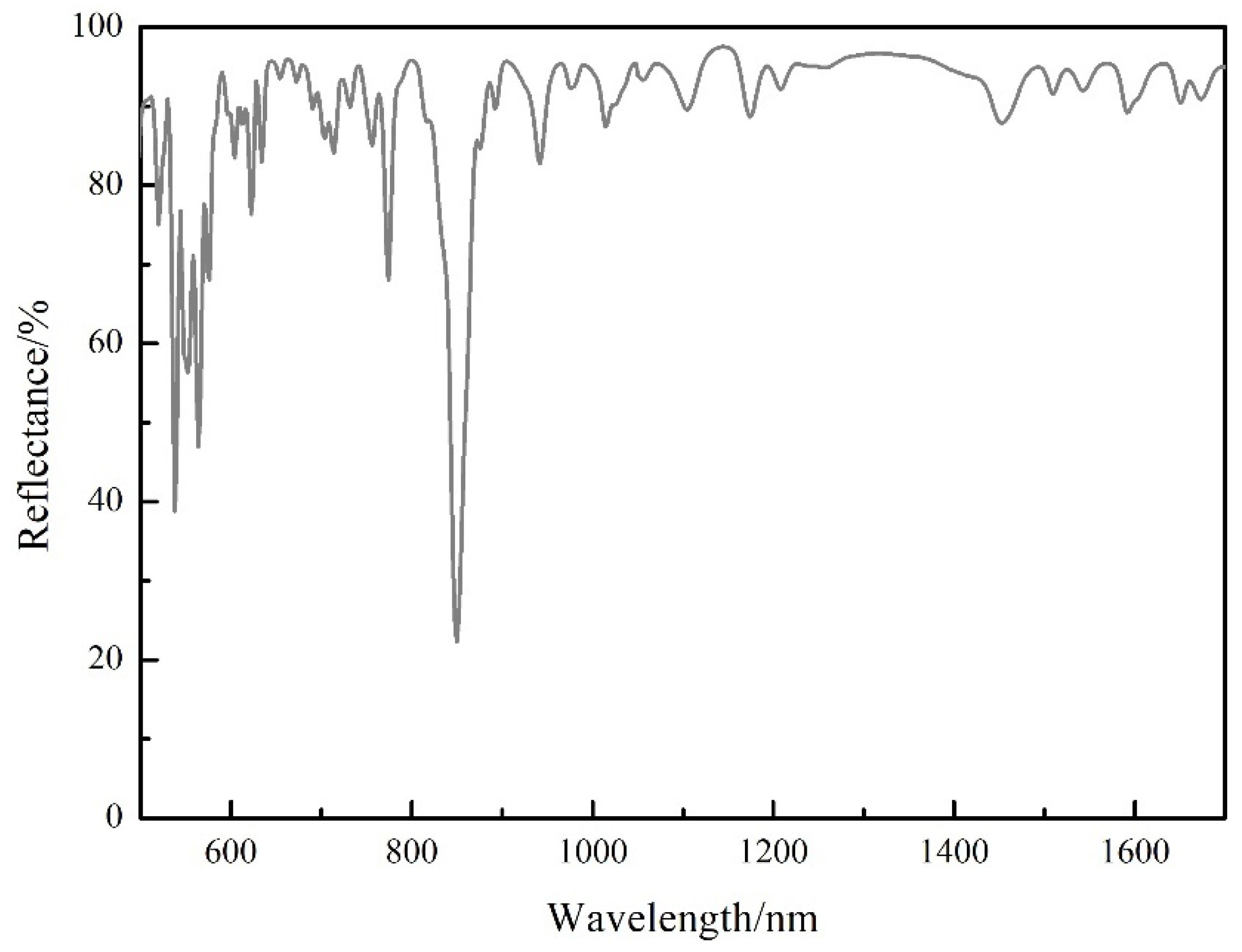
- Average reflectance: R > 85% in the 0.5–0.8 μm and 0.9–1.7 μm bands.
- •
- Surface profile precision maintained post-coating.
- •
- Coating uniformity ≥ 98%.
- •
- Antireflection (AR) coating performance:
- ○
- Average transmittance: T > 95% in the 3–5 μm and 8–12 μm bands.
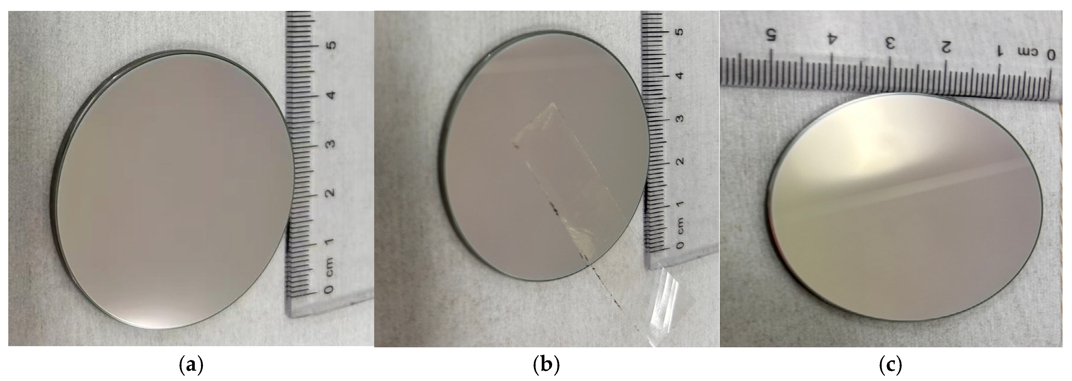
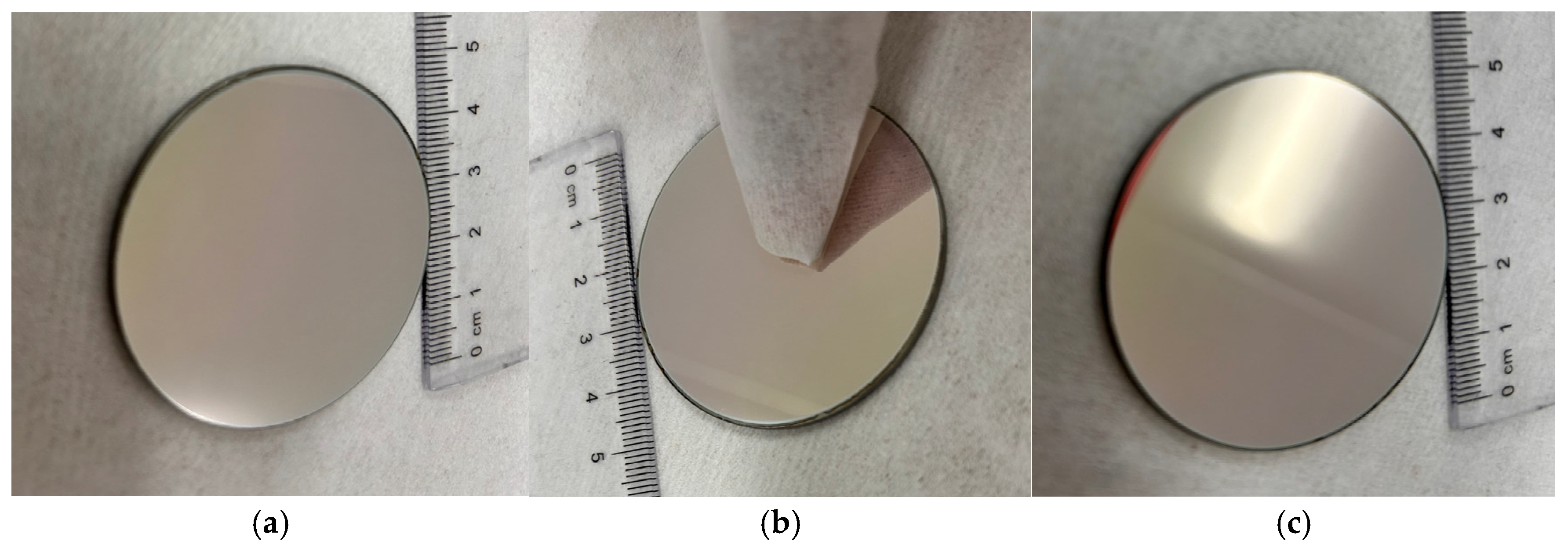
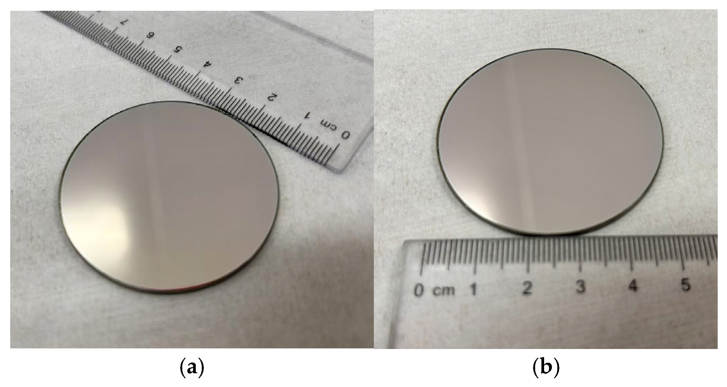
2. Experiment
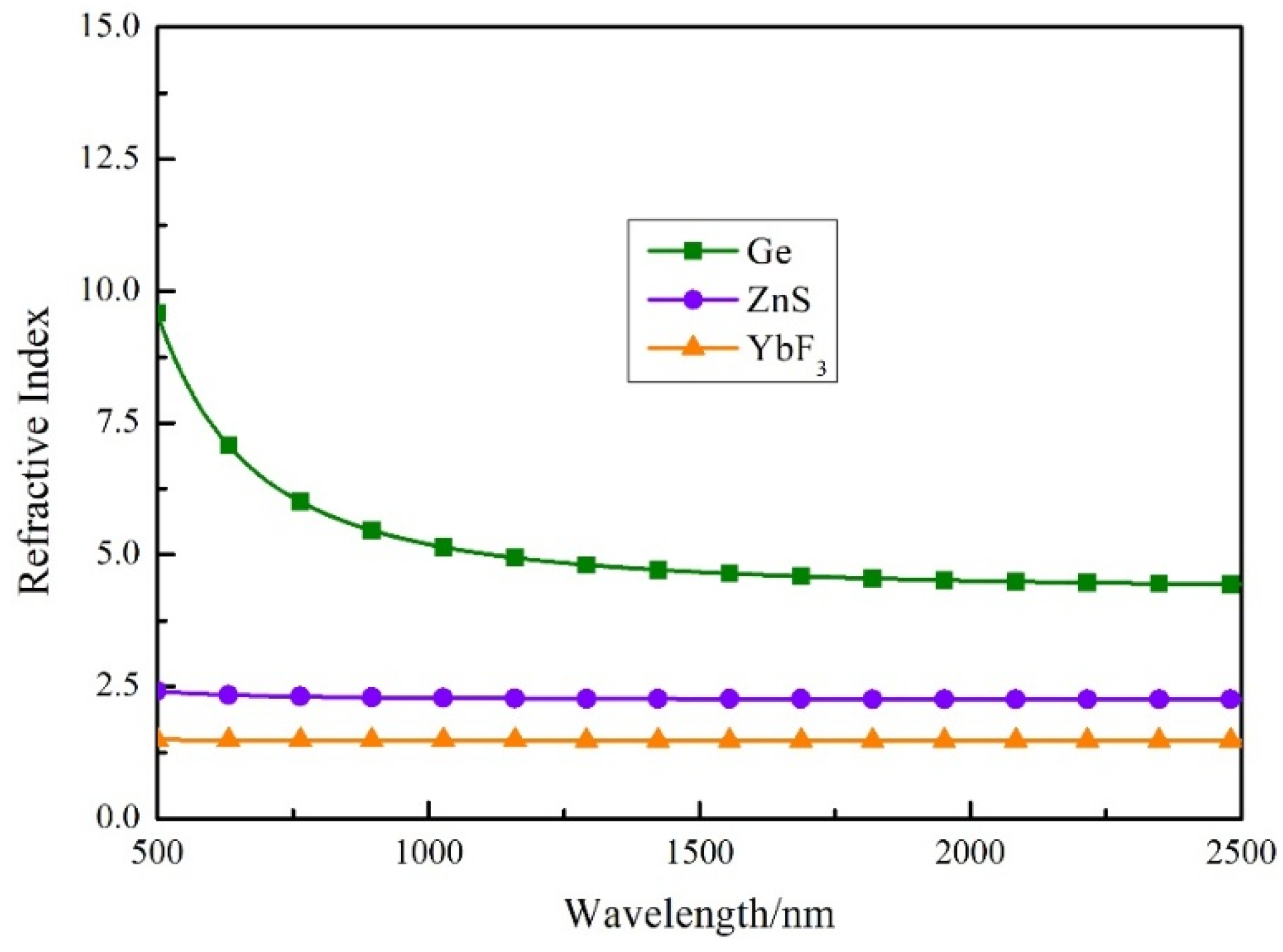
- •
- Ge: 4.4;
- •
- ZnS: 2.26;
- •
- YbF3: 1.48.
3. Results and Discussion
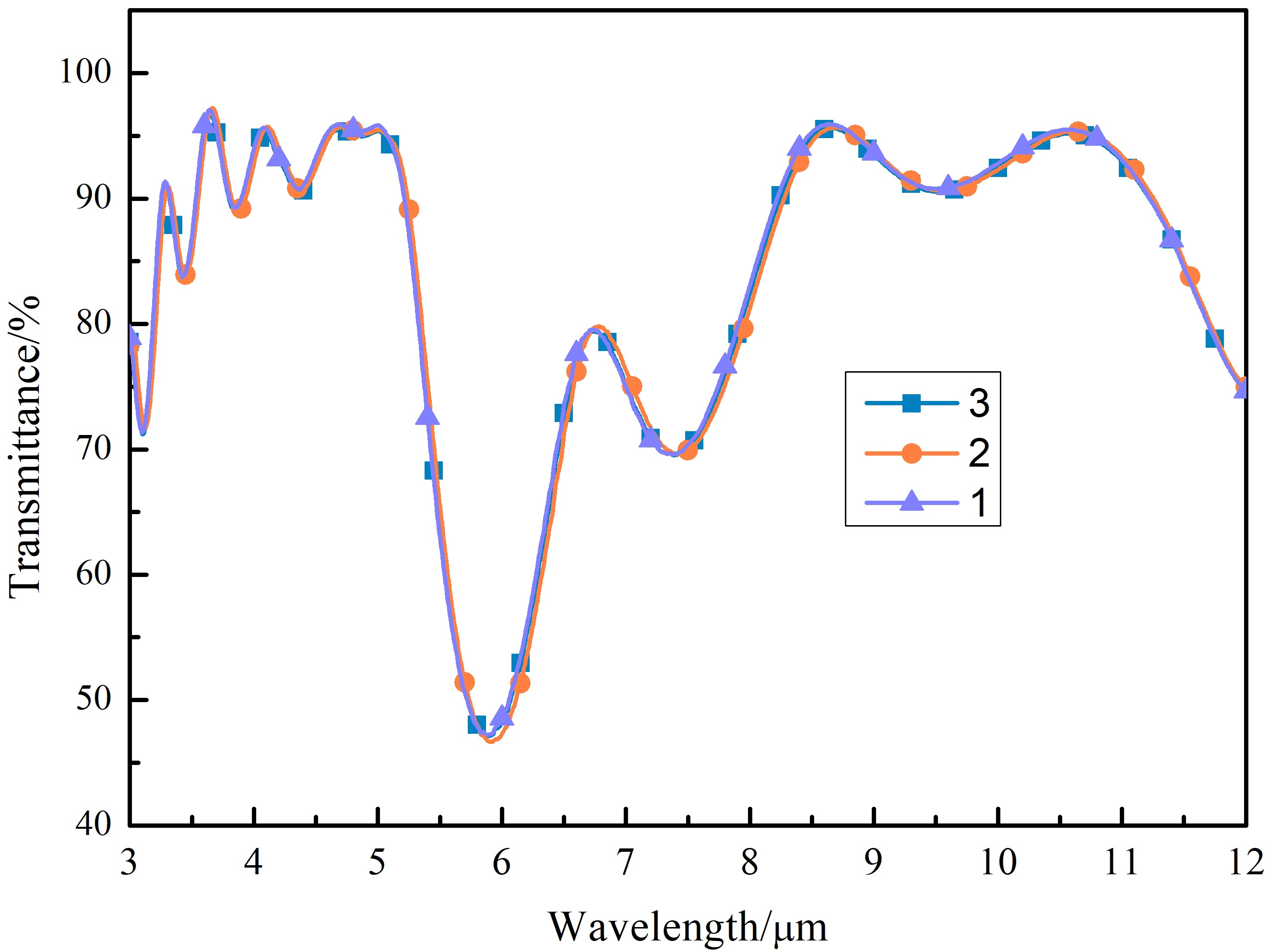
3.1. Design and Deposition of the Beam-Splitting Coating System
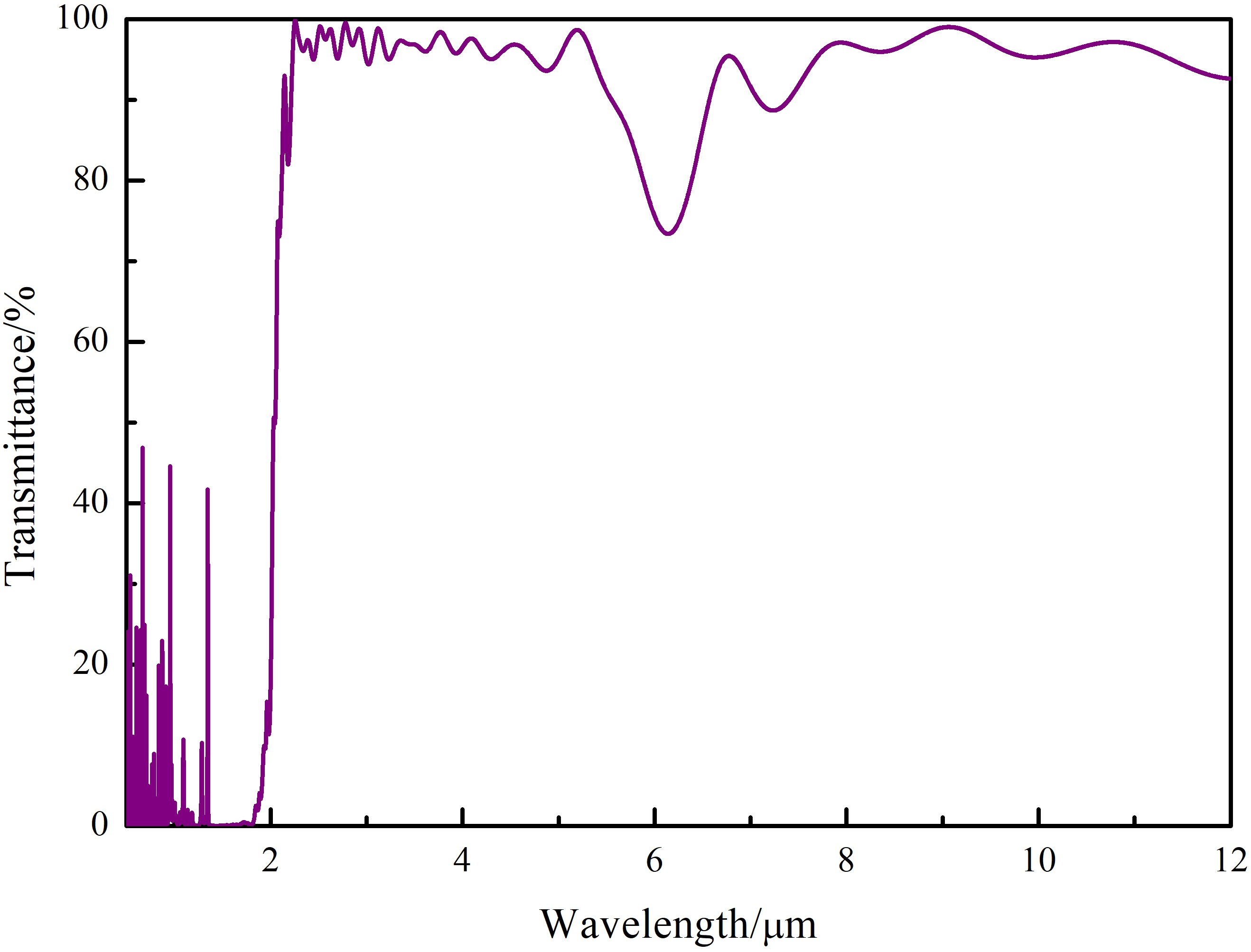
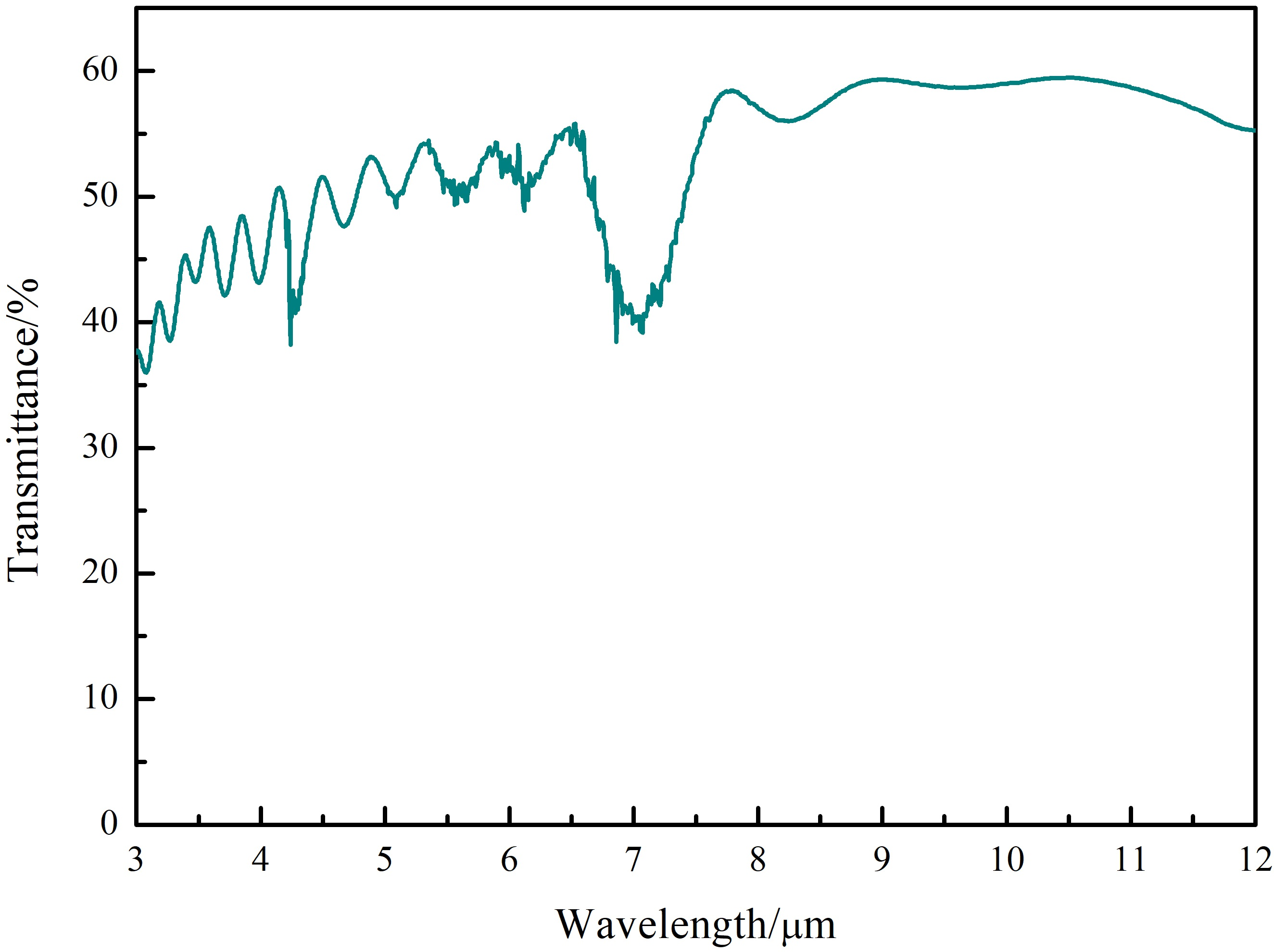
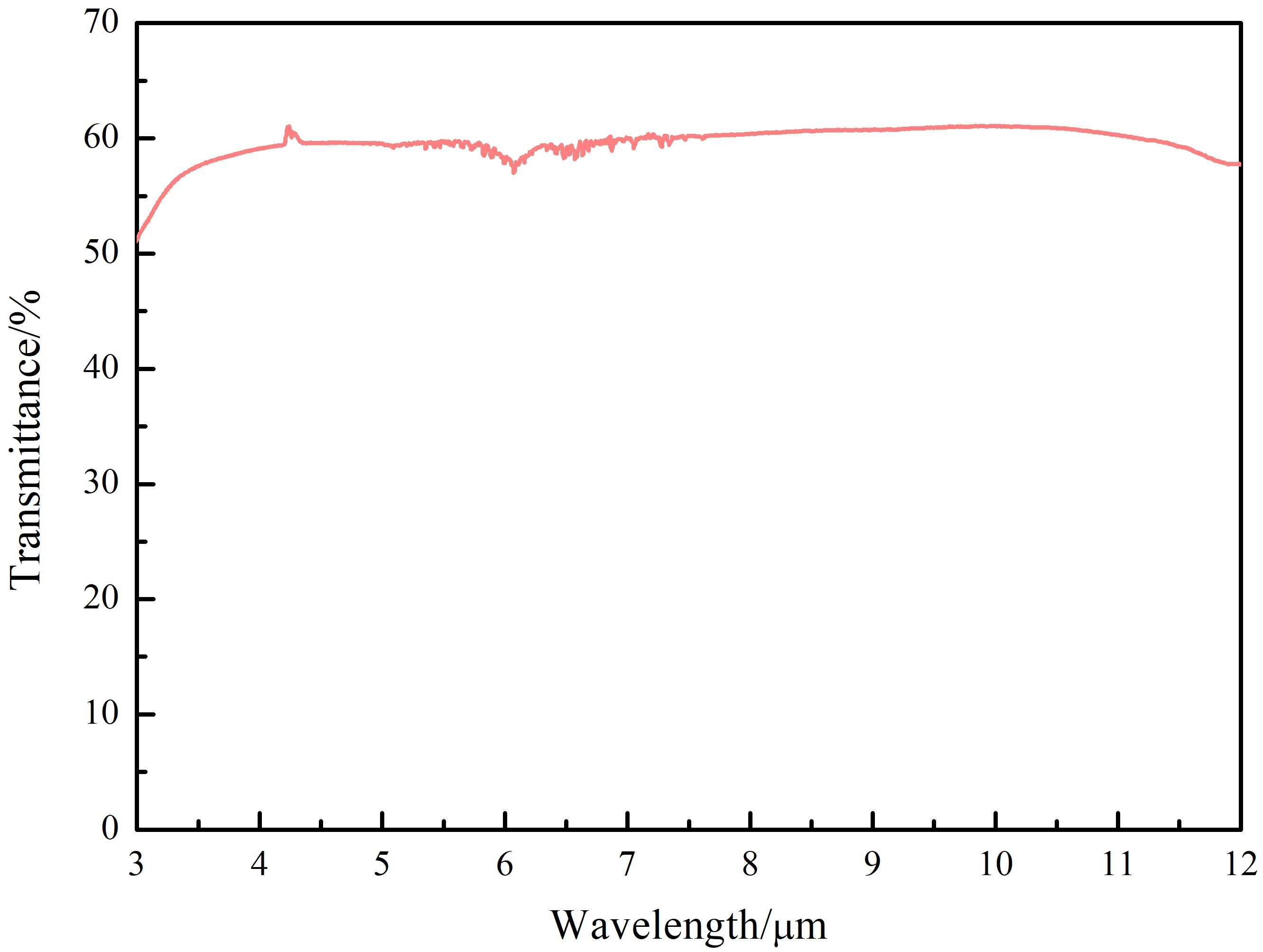
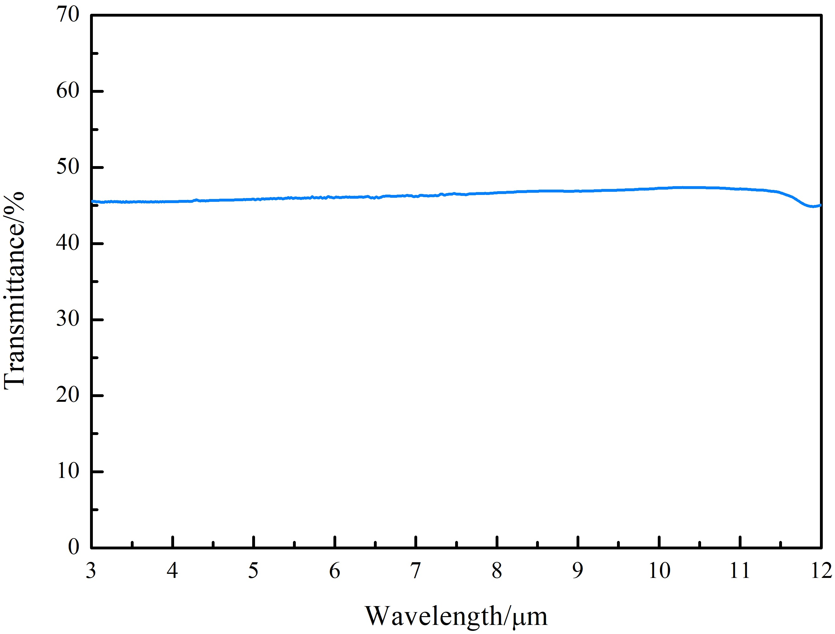
- The overall transmittance across the entire transmission band is relatively low.
- The transmittance in the 3–5 μm band exhibits a more significant decline, with particularly low values at shorter wavelengths.
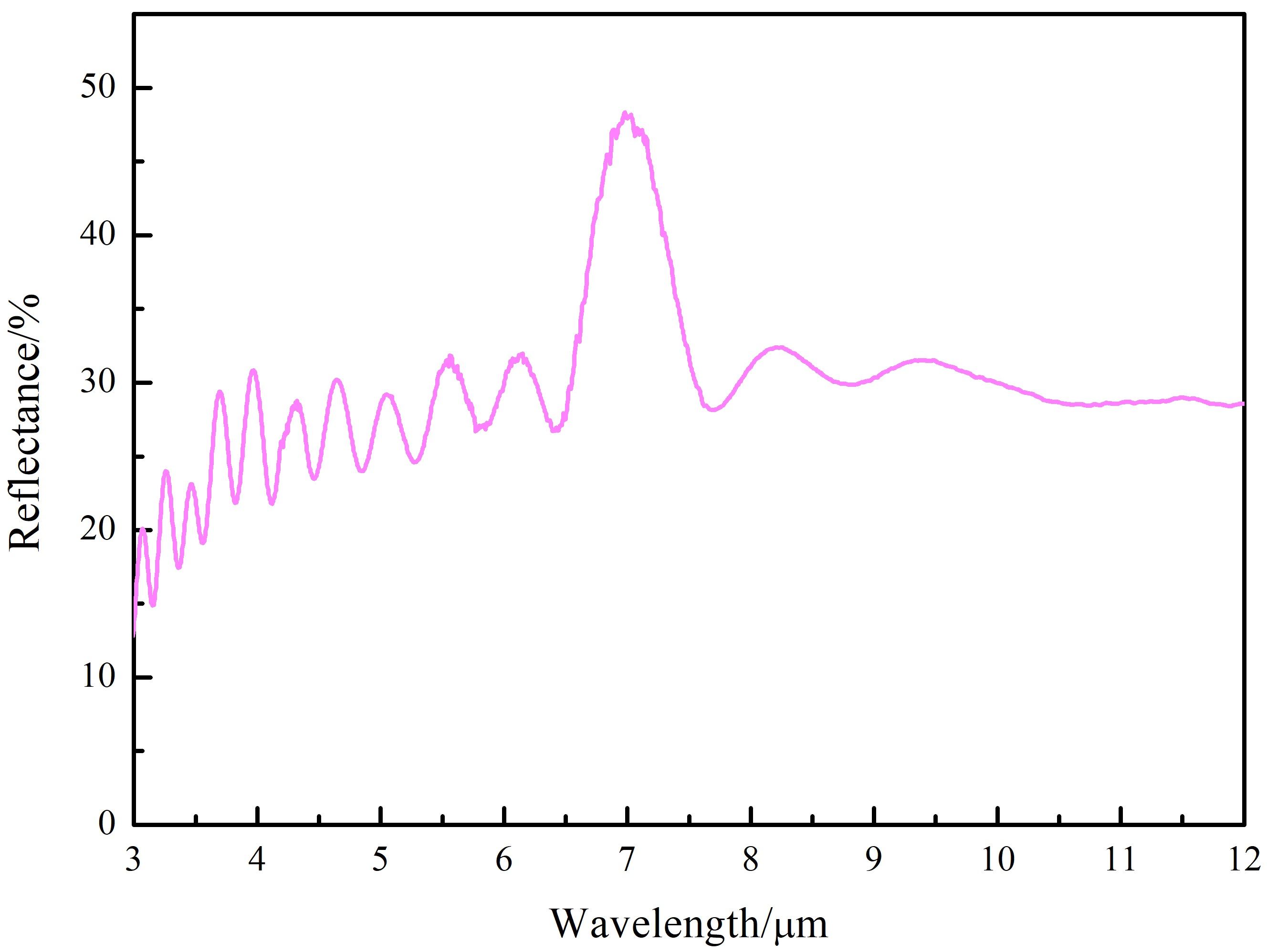
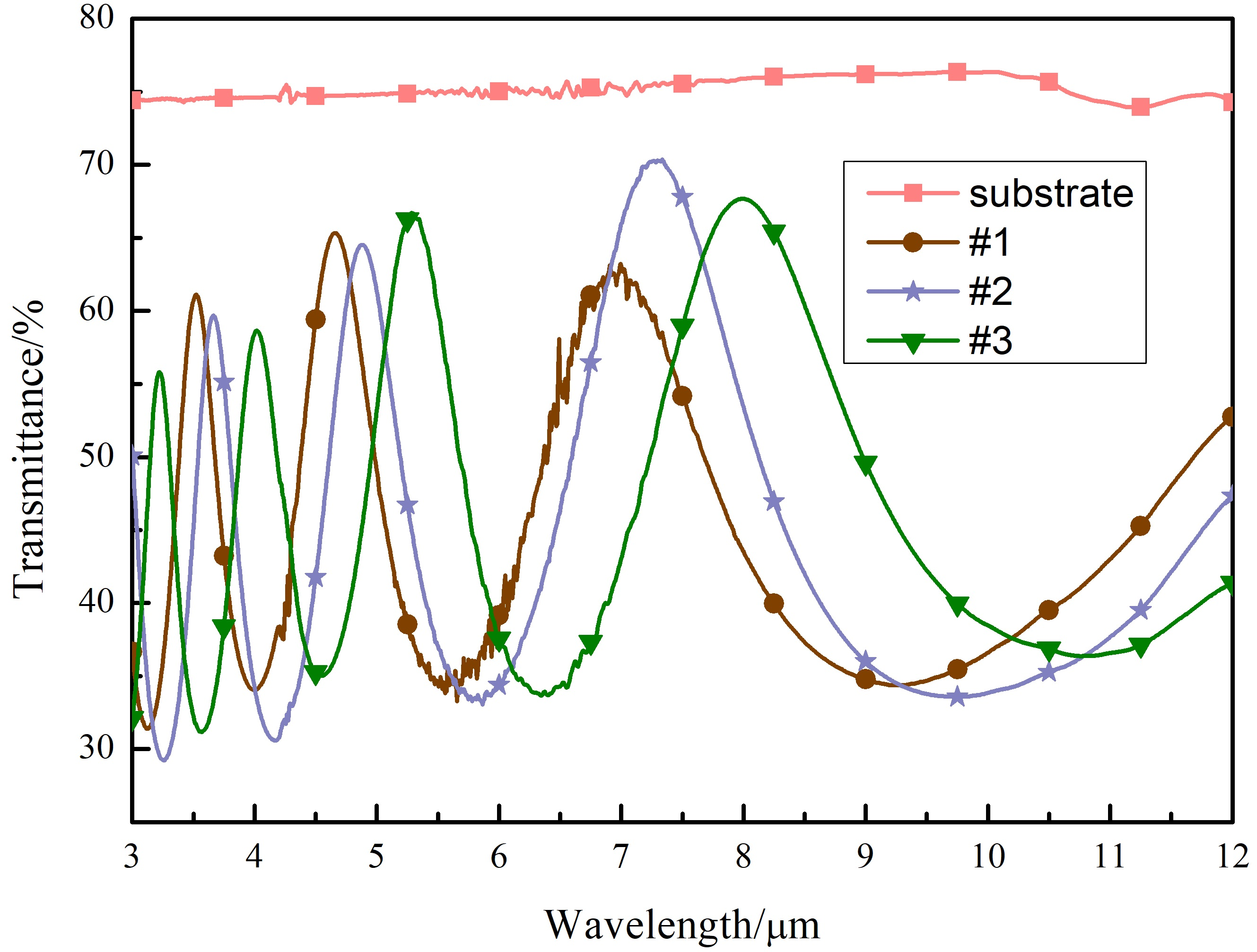
3.2. Investigation of Absorption Issues
- (1)
- Decomposition of ZnS at high temperatures
- (2)
- Sputtering contamination from the ion source
- (3)
- Cross-contamination between coating materials
- (4)
- High absorption of Ge at high temperatures
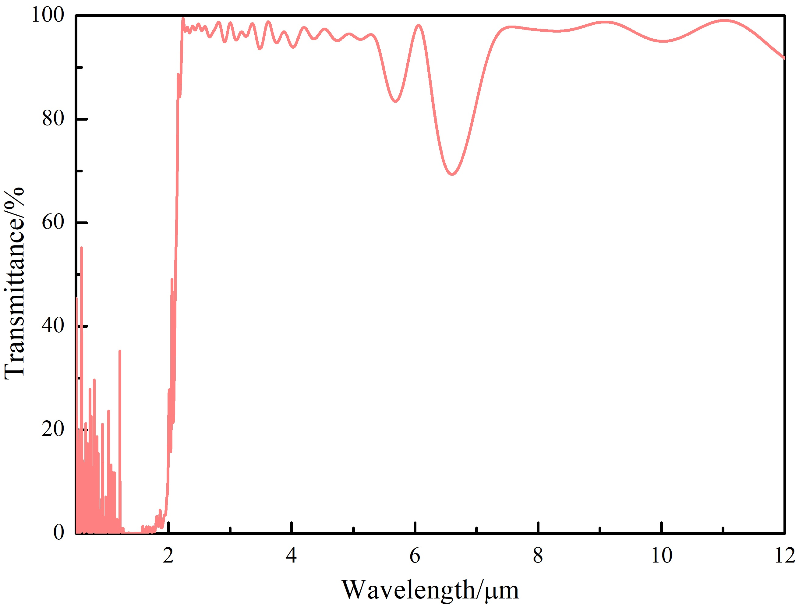
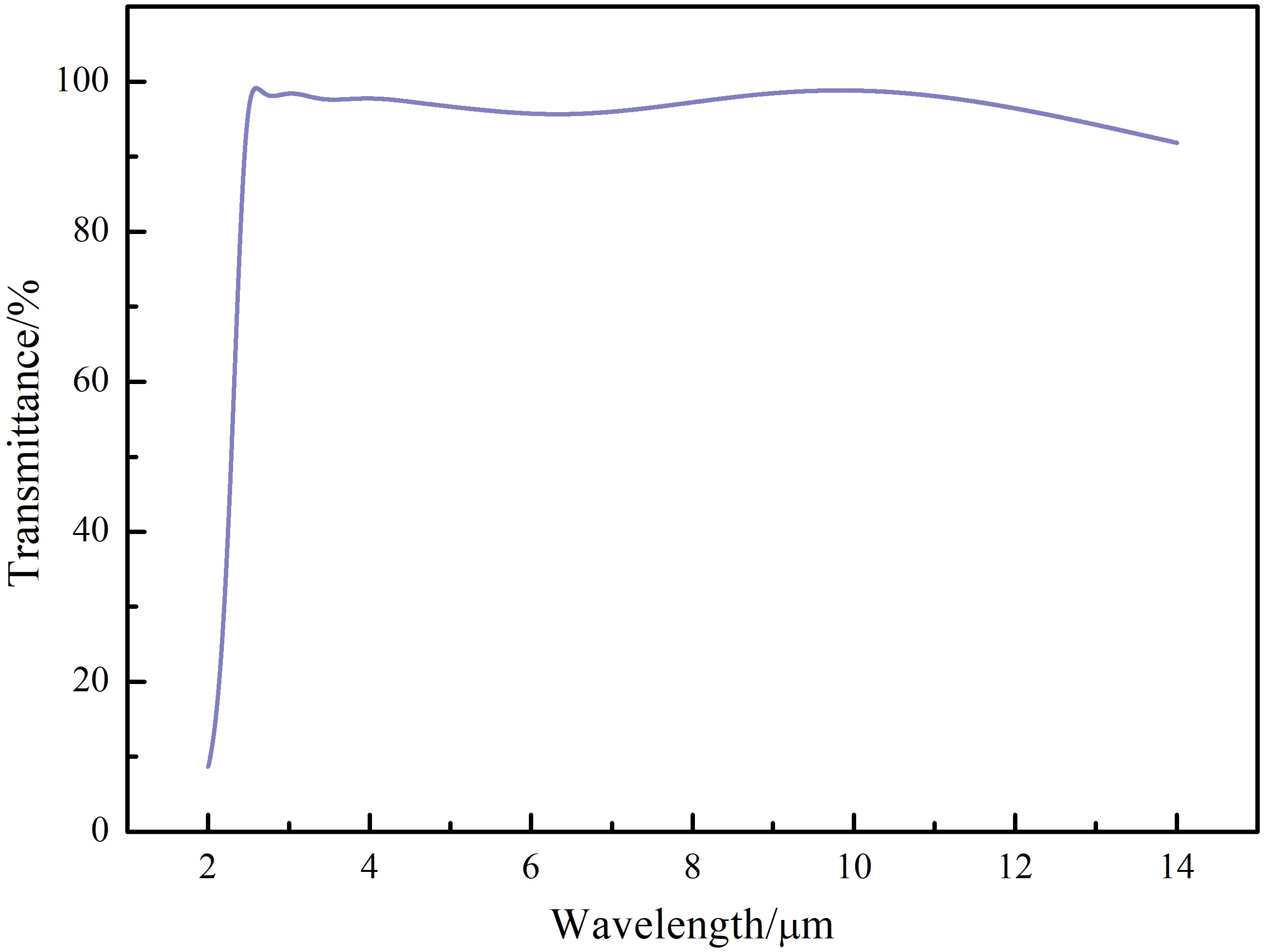
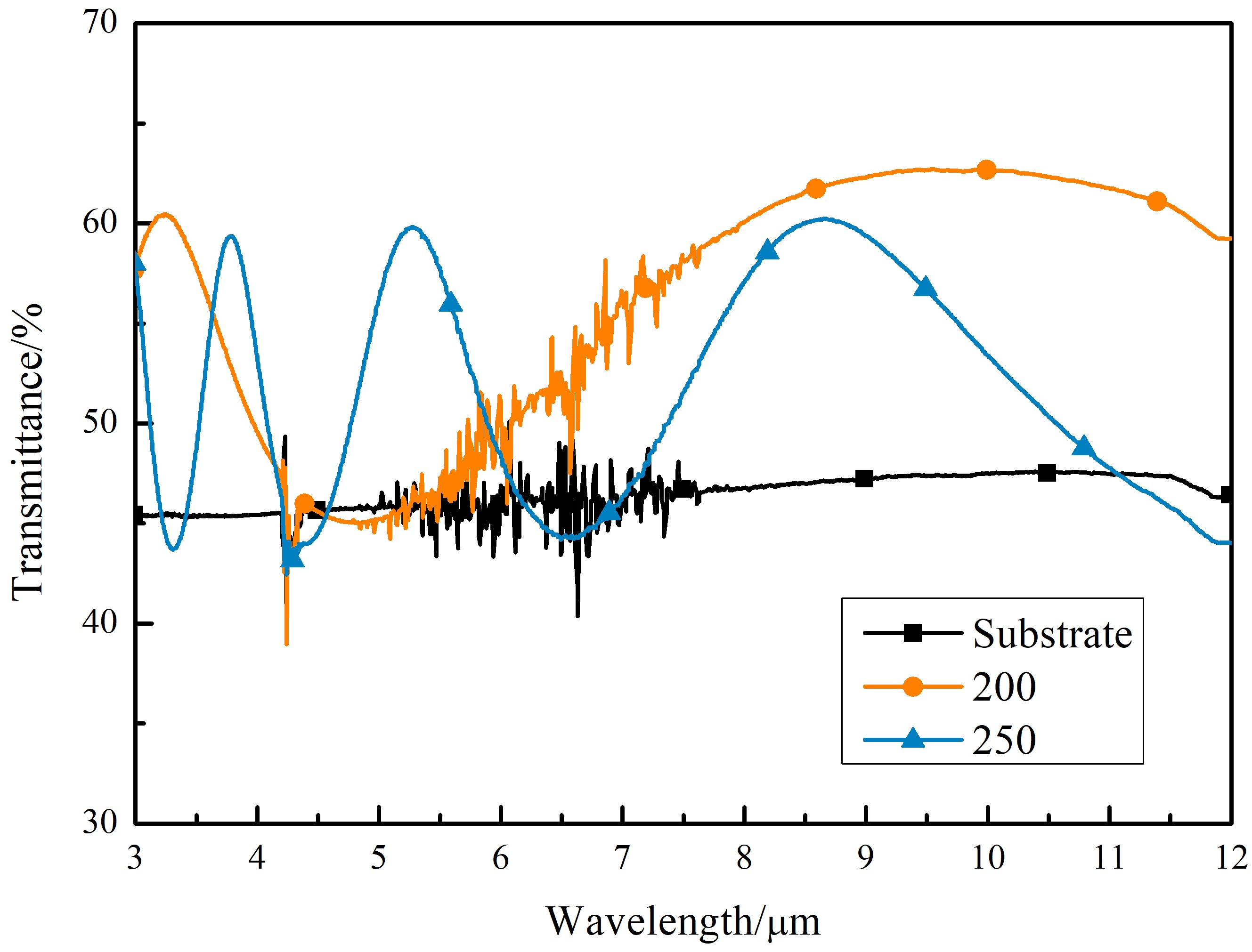
3.3. Optimization of the Coating System and Process
- •
- Tave@3–5 μm = 45.5%;
- •
- Tave@8–12 μm = 46.9%.
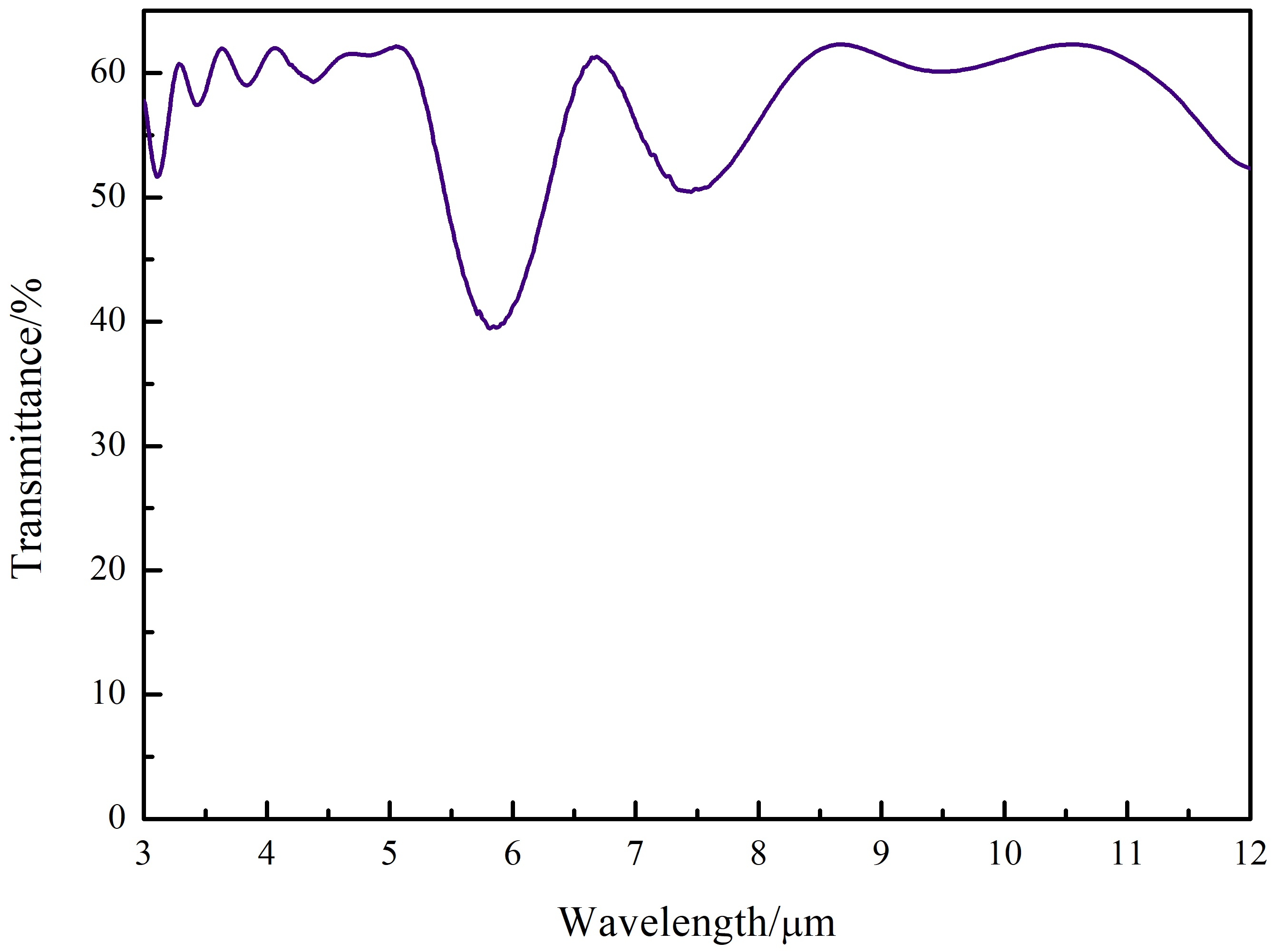
- •
- Tave@3–5 μm = 62.6%;
- •
- Tave@8–12 μm = 63.8%.
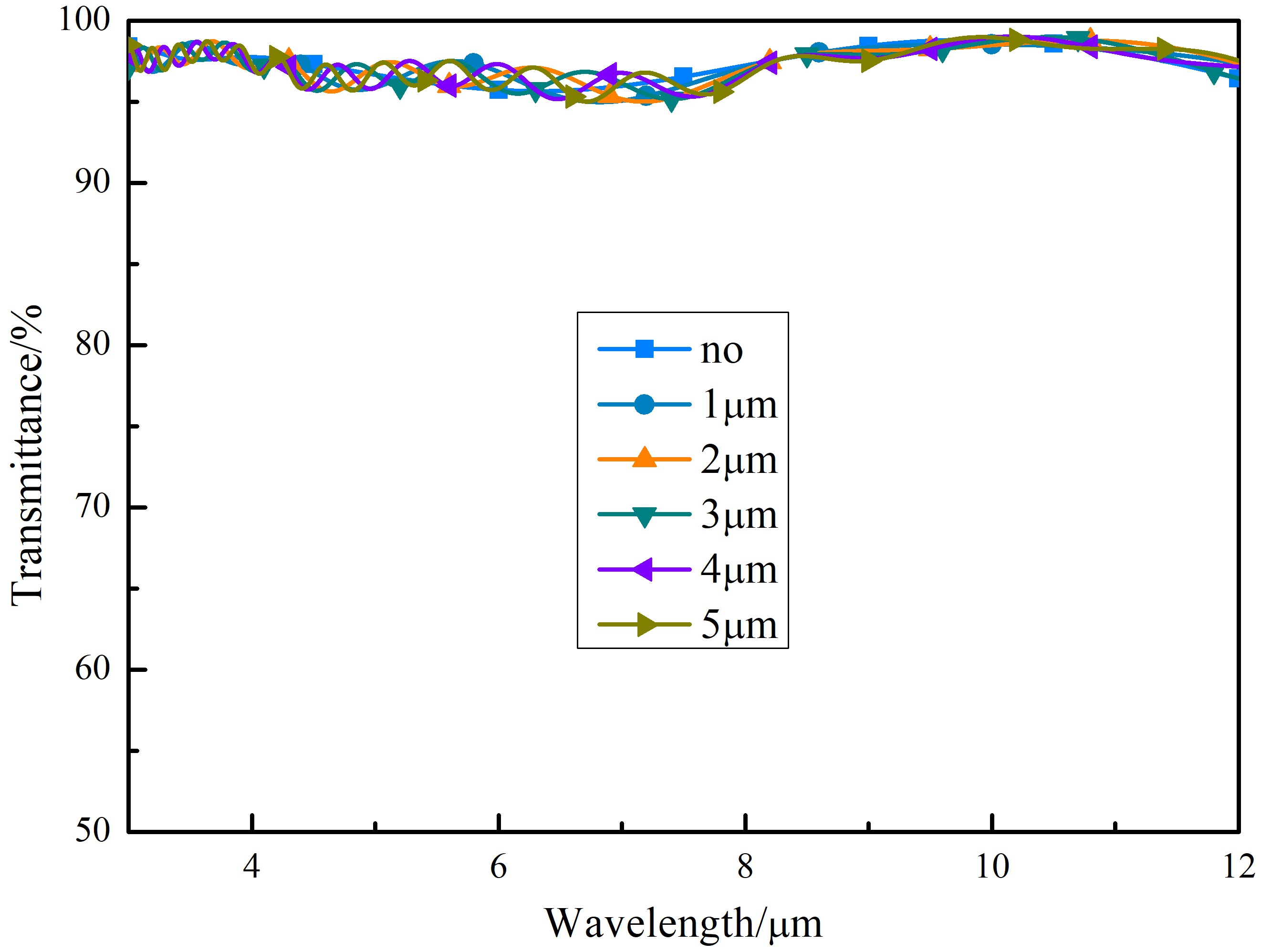
3.4. Non-Optical Properties of the Coatings
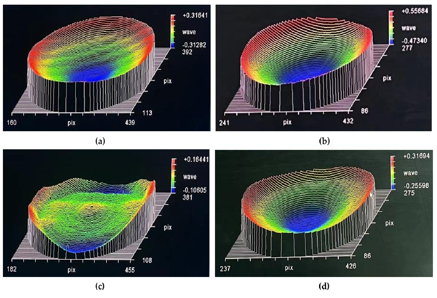
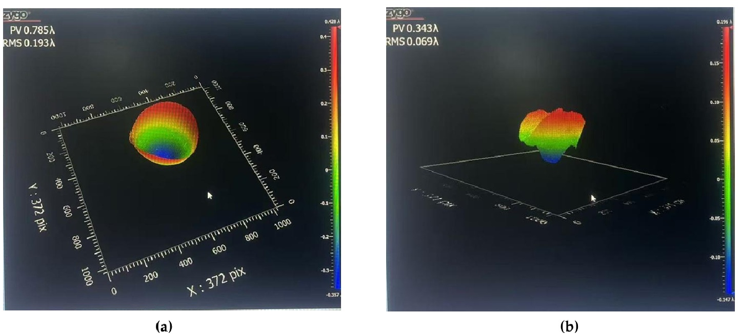
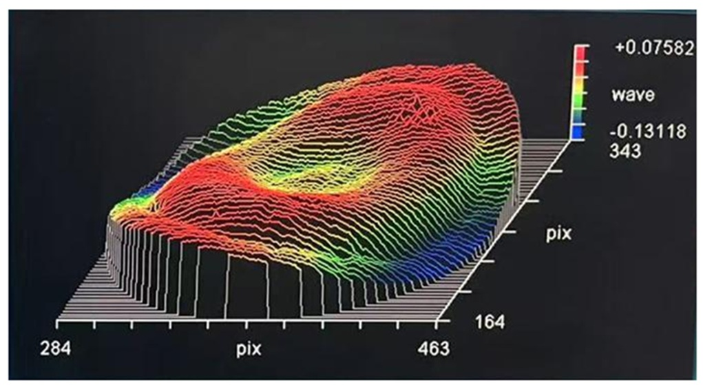
3.5. Surface Profile Correction
4. Conclusions
Author Contributions
Funding
Institutional Review Board Statement
Informed Consent Statement
Data Availability Statement
Conflicts of Interest
References
- Hawkins, G.J.; Sherwood, R.E.; Barrett, B.M.; Wallace, M.; Orr, H.J.B.; Matthews, K.; Bisht, S. High-performance infrared narrow-bandpass filters for the Indian National Satellite System meteorological instrument (INSAT-3D). Appl. Opt. 2008, 47, 2346–2356. [Google Scholar] [CrossRef] [PubMed]
- Ferrante, R.A.; Rand, T.W.; Cabrera, R.; Paloian, M.A. Visible/long-wave infrared dichroic beamsplitter. Opt. Eng. 2005, 44, 063801. [Google Scholar] [CrossRef]
- Li, Z.; Liu, H.; Sun, P.; Yang, X.; Bai, J.; Xu, Y.; Yang, S.; Ji, Y.; Su, J. Design and preparation of laser/long-wave infrared dual-band antireflection thin-film. Infrared Laser Eng. 2022, 51, 20210944. [Google Scholar]
- Habel, F.; Pervak, V. Dispersive mirror for the mid-infrared spectral range of 9–11.5 μm. Appl. Opt. 2017, 56, C71–C74. [Google Scholar] [CrossRef]
- Dogan, Y.; Erdogan, I.; Altuntepe, A. Design and fabrication of highly efficient antireflective coating in MWIR on germanium using ion-assisted e-beam deposition. Opt. Mater. 2024, 157, 116362. [Google Scholar] [CrossRef]
- Ghosh, A.; Upadhyaya, A.S. Broad band antireflection coating on zinc sulphide simultaneously effective in SWIR, MWIR and LWIR regions. Infrared Phys. Technol. 2009, 52, 109–112. [Google Scholar] [CrossRef]
- Duan, W.; Liu, D.; Zhang, F. Infrared dichroic filter used in multi-channel image-forming system. J. Infrared Millim. Waves 2008, 27, 397–400. [Google Scholar]
- Jiang, Y.; Liu, H.; Wang, L.; Chen, D.; Li, S.; Ji, Y. Design and preparation technology of laser protective film window of satellite. Chin. Opt. 2019, 12, 804–809. [Google Scholar] [CrossRef]
- Zhang, Y.; Wang, Y.; Sun, X.; Shen, W.; Liu, X.; Gu, P. Design and fabrication of short-wave/long-wave infrared dichroic beam splitter. Acta Opt. Sin. 2010, 30, 597–601. [Google Scholar] [CrossRef]
- Duan, W.; Liu, B.; Zhuang, Q.; Jiang, L.; Li, D.; Yu, D.; Qin, Y.; Ni, R.; Li, Y.; Zhou, S.; et al. Research progess of infrared thin film coatings applied in space remote sensing systems. Acta Opt. Sin. 2022, 51, 0951601. [Google Scholar]
- Zhang, J.; Sun, W.; Fu, X.; Pan, Y.; Wang, B.; Lin, Z.; Shi, P. Research on infrared ultrawideband beam splitter. J. Appl. Opt. 2024, 45, 1270–1276. [Google Scholar]
- Wang, S.; Zhang, J.; Mi, G.; Yin, W.; Liu, Q.; Zhao, H.; Zhang, X. Design method and application of wavelength error compensation for multi-band films. Vacuum 2024, 61, 7–14. [Google Scholar]
- Guan, Q.; Liao, L. Research of VIS/NIR/MIR multispectral anti-reflective hard window coatings on the sapphire substrate. Opt. Optoelectron. Technol. 2017, 15, 66–72. [Google Scholar]
- Liu, D.; Li, D.; Chen, G. Two methods for fabricating dichroic beam splitter with spectrum from visible light to thermal infrared. Infrared 2009, 30, 8–11. [Google Scholar]
- Yu, T.; Cheng, V.; Qin, Y.; Liu, D.; Zhang, F. Design and manufacture of broadband infrared antireflection coatings for Germanium windows. Acta Opt. Sin. 2010, 30, 1197–1200. [Google Scholar]
- Maudet, F.; Lacroix, B.; Santos, A.J.; Paumier, F.; Paraillous, M.; Dupeyrat, C.; Garcia, R.; Morales, F.M.; Girardeau, T. Towards perfect MWIR transparency using oblique angle deposition. Appl. Surf. Sci. 2019, 470, 943–950. [Google Scholar] [CrossRef]
- Duris, M.; Deubel, D.; Bodiou, L.; Paumier, F.; Vaudry, C.; Keromnes, J.-C.; Charrier, J. Fabrication of Ge-ZnS multilayered optical filters for mid-infrared applications. Thin Solid Film. 2021, 719, 138488. [Google Scholar] [CrossRef]
- Zhu, X.; Zhang, R.; Zheng, Y.; Wang, S.; Chen, L. Spectroscopic ellipsometry and its applications in the study of thin film materials. Chin. Opt. 2019, 12, 1195–1234. [Google Scholar]
- Amotchkina, T.; Trubetskov, M.; Schulz, M.; Pervak, V. Comparative study of NIR-MIR beamsplitters based on ZnS/YbF3 and Ge/YbF3. Opt. Express 2019, 27, 5557–5569. [Google Scholar] [CrossRef]
- Lu, J.; Liu, W.; Pan, Y. Optical Film Technology; Publishing House of Electronics Industry: Beijing, China, 2011; pp. 9–10. [Google Scholar]
- Chen, X.; Wu, Z.; Zhao, X.; Zhou, X.; Wang, D. Development of mid-infrared dual-channel filter. Opt. Instrum. 2020, 42, 32–39. [Google Scholar]
- Liu, D.; Liu, H.; Jiang, C.; Leng, J.; Zhang, Y.; Zhao, Z.; Zhuang, K.; Jiang, Y.; Ji, Y. Temperature dependence of the infrared optical constants of germanium films. Thin Solid Film. 2015, 592, 292–295. [Google Scholar] [CrossRef]
- Perez, G.; Bernal-Oliva, A.M.; Marquez, E.; Gonzalez-leal, J.M.; Morant, C.; Genova, I.; Trigo, J.F.; Sanz, J.M. Optical and structural characterization of single and multilayer germanium/silicon monoxide systems. Thin Solid Film. 2005, 485, 274–283. [Google Scholar] [CrossRef]
- Hotyynska, M.; Tighe, A.; Semprimoschnig, C. Coatings and thin films for spacecraft thermos-optical and related functional applications. Adv. Mater. Interfaces 2018, 5, 1701644. [Google Scholar] [CrossRef]
- GB/T 26332.4-2015; Optics and Photonics-Optical Coatings-Part 4: Specific Test Methods. Standards Press of China: Beijing, China, 2015.
- Amotchkina, T.; Trubetskov, M.; Hahner, D.; Pervak, V. Characterization of e-beam evaporated Ge, YbF3, ZnS, and LaF3 thin films for laser-oriented coatings. Appl. Opt. 2020, 59, A40–A47. [Google Scholar] [CrossRef]
- Richter, F.; Kupfer, H.; Schlott, P.; Gessner, T.; Kaufmann, C. Optical properties and mechanical stress in SiO2/Nb2O5 multilayers. Thin Solid Film. 2001, 389, 278–283. [Google Scholar] [CrossRef]


| Materials | Rate (Å/S) | Temperature (°C) | Anode Voltage (V) | Cathode Current (A) |
|---|---|---|---|---|
| Ge | 5 | 150 | 100 | 1 |
| ZnS | 10 | 150 | 100 | 1 |
| YbF3 | 6 | 150 | 200 | 2.5 |
| Symbol | Coating Structure | Central Wavelength/nm | Thickness/μm |
|---|---|---|---|
| S1 | Ge/(0.5HM0.5H)8 0.8(0.5ML0.5M)8 0.63(0.5ML0.5M)8 0.5(0.5ML0.5M)8 0.4(0.5ML0.5M)8 0.3(0.5ML0.5M)8/Air | 1800 | 14.02 |
| S2 | Ge/(0.5HM0.5H)9 2M 0.8(0.5ML0.5M)8 0.63(0.5ML0.5M)8 0.49(0.5ML0.5M)8 0.39(0.5ML0.5M)9 0.31(0.5ML0.5M)9/Air | 1800 | 13.16 |
| Substrate | Ion Source Energy | C Atomic Composition Percentages | Fe Atomic Composition Percentages | Cr Atomic Composition Percentages |
|---|---|---|---|---|
| #1 | 280 V, 8 A | 38.21 | 10.51 | 3.99 |
| #2 | 250 V, 5 A | 35.36 | 9.26 | 8.13 |
| #3 | 200 V, 4 A | 35.16 | 2.83 | 3.68 |
| Number | Process |
|---|---|
| #1 | No ion source, temperature 250 °C |
| #2 | Ion source, temperature 250 °C |
| #3 | Ion source, temperature 150 °C |
| Number | RMS/μm (Substrate) | RMS/μm (After sp Coating) | RMS/μm (Deviation) |
|---|---|---|---|
| #3 | 0.099 | 0.166 | 0.066 |
| #8 | 0.026 | 0.083 | 0.056 |
| Number | RMS/μm (Before) | RMS/μm (After) | RMS/μm (Deviation) |
|---|---|---|---|
| #3 | 0.166 | 0.156 | −0.010 |
| #8 | 0.082 | 0.073 | −0.009 |
Disclaimer/Publisher’s Note: The statements, opinions and data contained in all publications are solely those of the individual author(s) and contributor(s) and not of MDPI and/or the editor(s). MDPI and/or the editor(s) disclaim responsibility for any injury to people or property resulting from any ideas, methods, instructions or products referred to in the content. |
© 2025 by the authors. Licensee MDPI, Basel, Switzerland. This article is an open access article distributed under the terms and conditions of the Creative Commons Attribution (CC BY) license (https://creativecommons.org/licenses/by/4.0/).
Share and Cite
Shi, Y.; Li, H.; Zhang, S.; Luo, C.; Sun, J.; Lv, C.; Ding, J.; Yao, Y. Design and Deposition of Ultra-Broadband Beam-Splitting Coatings. Coatings 2025, 15, 695. https://doi.org/10.3390/coatings15060695
Shi Y, Li H, Zhang S, Luo C, Sun J, Lv C, Ding J, Yao Y. Design and Deposition of Ultra-Broadband Beam-Splitting Coatings. Coatings. 2025; 15(6):695. https://doi.org/10.3390/coatings15060695
Chicago/Turabian StyleShi, Yunyun, Haochuan Li, Sibao Zhang, Changxin Luo, Jiangheng Sun, Chenrui Lv, Jiaoteng Ding, and Yongsheng Yao. 2025. "Design and Deposition of Ultra-Broadband Beam-Splitting Coatings" Coatings 15, no. 6: 695. https://doi.org/10.3390/coatings15060695
APA StyleShi, Y., Li, H., Zhang, S., Luo, C., Sun, J., Lv, C., Ding, J., & Yao, Y. (2025). Design and Deposition of Ultra-Broadband Beam-Splitting Coatings. Coatings, 15(6), 695. https://doi.org/10.3390/coatings15060695