Article

Investigating the Microstructural Behavior and Energy Absorption of Pure Copper Lattice Structures Fabricated by Selective Electron Beam Melting

1
Advanced Materials Additive Manufacturing Innovation Research Center, Hangzhou City University, Hangzhou 310015, China
2
Zhejiang-Thailand International Joint Laboratory on New Materials Digital Design and Processing Technology, Hangzhou City University, Hangzhou 310015, China
3
College of Engineering, Hangzhou City University, Hangzhou 310015, China
4
College of Materials Science and Engineering, Xi’an University of Technology, Xi’an 710048, China
5
College of Mechanical Engineering, Zhejiang University of Technology, Hangzhou 310014, China
*
Author to whom correspondence should be addressed.
Coatings 2025, 15(3), 348; https://doi.org/10.3390/coatings15030348
Submission received: 24 February 2025 / Revised: 8 March 2025 / Accepted: 11 March 2025 / Published: 18 March 2025

Abstract

:
Pure copper’s exceptional thermal and electrical properties, along with its processability, make it indispensable in aerospace, automotive, and electrical industries, particularly in heat exchangers and radiators. Lattice structures, with high specific surface areas, low weight, and high strength, are ideal for lightweight yet strong components. While traditional methods struggle with complex lattice geometries, selective electron beam melting (SEBM) enables the fabrication of intricate pure copper lattices with high energy efficiency in a vacuum environment. This study used SEBM to fabricate OCTET pure copper lattices with relative densities of 21.16%–73.77%. The macrostructure matched the design, achieving a maximum energy absorption capacity of 15.00 MJ/m3. At 40.04% relative density, compressive response shifted from shock to compression hardening, with densification strains ranging from 23.96% to 51.68%. Microdefects such as corrugation, size differences, and internal holes influenced mechanical properties and energy absorption. Post-polishing reduced surface roughness from 14.12 μm to 2.70 μm without affecting specific energy absorption. Increasing strut diameter reduced the microdefects’ impact on lattice strength, enhancing performance and reliability.

1. Introduction

Pure copper boasts excellent electrical conductivity (58 × 106 S/m), thermal conductivity (400 W/(m·K)), and machinability, making it an ideal material for heat exchangers and inductors [1,2,3]. With the rapid development of the electronics and electric vehicle industries, there is a trend toward miniaturizing and integrating radiators and inductors. Consequently, the development of lightweight and efficient pure copper components has become a significant focus.
Pure copper porous components offer customizable strength and stiffness, adjustable effective thermal conductivity, and catalytic efficiency. These properties ensure the stability of aerospace devices while maximizing payload and providing high specific strength, like the porous ceramics [4]. Additionally, they offer vehicles high energy absorption capacity against impacts [5]. Porous copper is applicable in thermal management devices, electrocatalytic materials, and batteries in spacecraft. Effective thermal management is crucial in aerospace devices to prevent overheating or thermal deformation of critical instruments due to the heat generated by power generation and electronic equipment during operation. Porous materials can reduce thermal conductivity paths while enhancing the thermal conductivity and isotherm of the material as a heat pipe component. In electrocatalysis, copper shows great promise in reducing carbon dioxide to produce hydrocarbons, thereby contributing to the reduction of greenhouse gas emissions [6]. In the field of batteries, porous pure copper materials can also serve as fluid collectors for anodeless lithium batteries [5]. However, the complex lattice porous structure is challenging to prepare using traditional processing methods such as casting and forging. Additive manufacturing (AM) addresses this challenge by building parts layer by layer with powdered raw materials, enabling rapid production of parts with complex structures, reducing production costs, and shortening processing cycles [7,8]. AM has emerged as a core technology of the fourth industrial revolution among other advanced technologies [9].
Among metal additive manufacturing technologies, selective laser melting (SLM) and selective electron beam melting (SEBM) are the most widely used [10,11]. Most SLM devices use red lasers as the energy source, but the reflectivity of pure copper to red light is as high as 90%, making it difficult to produce dense pure copper parts with this technology. Additionally, the reflected laser can damage the device [12,13,14]. Colopi et al. [15] found that increasing the laser power to over 500 W can transfer more heat to the material, forming a stable molten pool. However, this also increases the risk of machine component damage due to the reflected laser. Green and blue lasers, which have lower reflectivity and energy absorption rates of 20%–60%, are also used as energy sources [16,17].
SEBM offers significant advantages in the preparation of pure copper. The electron beam used as the energy source has a higher energy absorption rate (over 80%). The vacuum environment prevents contamination during processing and maintains a high temperature, reducing the temperature gradient during cooling and minimizing internal stress [2,18]. Guschlbauer et al. [2] successfully prepared a sample with a density of 99.95% by controlling process parameters, resulting in elongated coarse columnar crystals and a strong cube texture from epitaxial grain growth. The hardness was about 50 HV0.5, the tensile yield strength was about 65 MPa, and the elongation at break was about 50%, similar to the properties of cold-rolled and annealed copper. Megahed et al. [19] studied the effect of energy density on the forming quality of SEBM pure copper, finding that at an area energy density of 8.64 J/mm², the relative density of pure copper reached 99.99%, with the average grain size increasing with energy density. Frigola et al. [20] also successfully prepared internal cooling runner parts with complex geometries. Ramirez et al. [21] used the SEBM technology to prepare a random open-cell foam with densities ranging from 0.73 to 6.67 g/cm3 and net lattice pure copper porous structures. The stiffness or Young’s modulus of the pure copper open-cell foam structures varied with density, consistent with the Gibson–Ashby foam model. Yang et al. [22] used the SEBM technology to form a pure copper reentrant lattice structure, observing that strut yield appeared early in compression experiments. After two layers of aging, the pure copper lattice sample began to densify. Due to the excellent ductility of pure copper, the struts did not necessarily break but acted as resistance sites for further deformation, promoting densification. The size of the pure copper struts changed by more than 13%, with observed pore and step effects resulting in a smaller effective strut size. The high thermal conductivity of copper also made the sintering effect significant, degrading the surface quality of the SEBM pure copper samples. This disparity between theoretical predictions and actual mechanical properties can be attributed to these factors. Therefore, surface polishing of the lattice structure is needed to eliminate the influence of surface quality on the properties of the lattice structure.
The relative density of a lattice structure is closely related to its compressive deformation mode. Chen et al. [23] prepared Ti6Al4V OCTET lattice structure materials and found that the deformation mode changed when the relative density was between 22% and 23%. The length–diameter ratio of a single cell also affects the compressive deformation of lattice structures and their mechanical properties. Tancogne et al. [24] simulated the compression properties of 316L OCTET lattice structures formed by SLM using the finite element method. They found that when the relative density was less than 30%, the compression response showed an unstable distortion mode, and when the relative density exceeded 30%, the compression response transitioned to a stable non-buckling mode. The specific energy absorption capacity increased with relative density. Zhao et al. [25] found that as the length–diameter ratio increased, the deformation mode of the lattice structure changed from layer-by-layer and overall deformation to 45° shear deformation, resulting in decreased energy absorption capacity. These findings indicate that different materials influence the compressive deformation of lattice structures in distinct ways. The compressive deformation and mode of pure copper OCTET lattice structures remain unclear. Masta et al. [26] studied the fracture toughness of OCTET lattice structures with a relative density of 8%–19% and found that toughness increases linearly with the square root of the relative density, that it is influenced by cell size, and that strength is proportional to relative density. As tension-oriented materials with low relative density, OCTET lattice structures lack stability and exhibit low buckling response under large strain deformation. Currently, there is limited research on the structural properties of pure copper OCTET lattices.
Thus, the purpose of this study was to investigate the compression properties of pure copper OCTET structures, regulate relative density by varying the column strut and cell size, and explore the effect of relative density on the macroscopic stress–strain response under uniaxial compression. Additionally, the study examined the impact of polishing on the mechanical properties of lattice structures.

2. Experiment

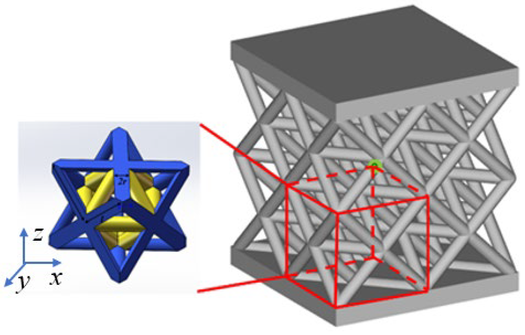
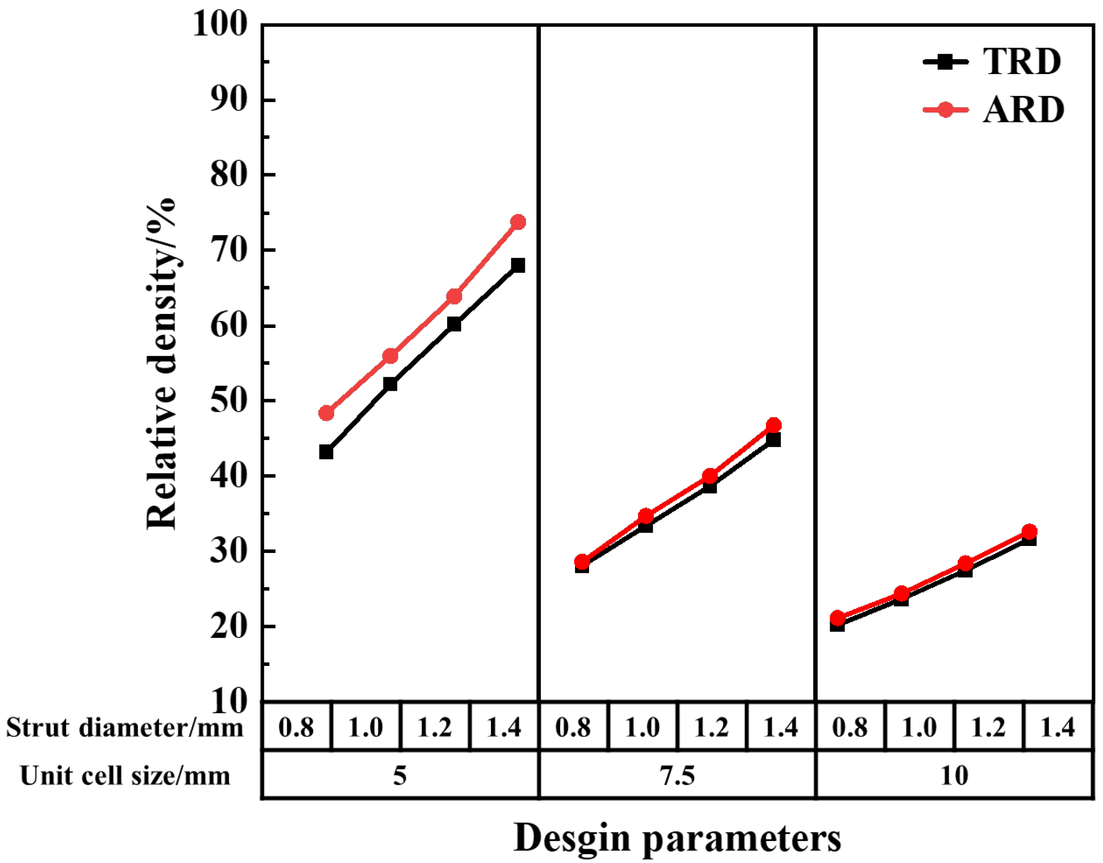
2.1. Lattice Structure Design and Relative Density

The lattice struts were designed with diameters of 0.8 mm, 1.0 mm, 1.2 mm, and 1.4 mm. To enhance the performance of the lattice structure, a solid metal plate with a thickness of 1.5 mm was added to both the upper and lower sides. The cell sizes were designed to be 5 mm, 7.5 mm, and 10 mm. The overall lattice structure was configured as a 2 × 2 × 2 sandwich array. The design model is illustrated in Figure 1.
Relative density ρrel is the volume ratio between the porous structure and the solid structure of the same size. It is an important parameter to measure the porous structure, which can be calculated as follows [27]:
ρ rel = V V 0 × 100 ,
where V0 is the volume of the bulk material at the same size (mm3) and V is the volume of the lattice structure (mm3).
The volume of the designed lattice structure was obtained using the Magics 21.0 software, and its relative density was calculated using a specified formula. The results are presented in Table 1. Sample numbers a–b are defined by cell size and strut diameter, where a represents the cell size and b represents the strut diameter. The designed relative density of the lattice structure ranged from 20.25% to 68.21%.

2.2. Sample Preparation

In this study, gas-atomized T2 pure copper powder (grade CW004A, conforming to the ASTM B170 standard [28]) with a particle size range of 45–105 μm was used as the raw material. The powder exhibited a spherical morphology, and the chemical composition of the powder, as provided by the supplier, included ≥99.9 wt.% Cu + Ag and trace impurities (e.g., Fe, Pb). The powder was sieved to ensure uniformity before processing. The pure copper samples were produced using a Sailong-Y150 electron beam selective melting equipment from Xi’an Sailong Company. The models were created using the SolidWorks 2022 software and then arranged using Magics 21.0. After layout, the file was saved in the STL format and sliced with SL-EBM Build Prepare 1.5.1. The sliced file was then imported into the device’s printing program. A 316L stainless steel substrate was used for printing. The substrate was leveled, and printing parameters were set to start preheating at 300 °C with a 90° rotated scanning strategy. The main process parameters are shown in Table 2. After preparation, the sample was cleaned using a powder recycle system (PRS) to remove any remaining powder.

2.3. Sample Performance Testing Methodology

For the measurement of microstructural characterization, the metallographic sample preparation involved sanding the sample with 80# to 2000# sandpaper, followed by polishing with a 0.5 μm polishing agent on a cashmere cloth. Polishing continued until surface scratches disappeared, achieving a mirror-like finish. The sample was then etched using a solution of 100 mL H2O, 19 g Fe(NO3)3, and 100 mL C2H5OH for 5–10 s. The samples were observed using an Olympus metallographic microscope. Electron backscatter diffraction (EBSD) was employed to characterize the microstructure of the pure copper lattice samples, with a step size of 3.6–4.0 μm.
Then, the surface polishing process was carried out as follows. The lattice structure was polished using an N9710S magnetic polishing machine from Aochen Technology Company for 10 min. An OLS5000 laser confocal microscope was then used to measure the surface roughness and morphology of the sample before and after polishing, allowing for a comparison of the polishing effects on the sample surface.
To obtain the mechanical properties, a Zwick Z005 universal testing machine (maximum load, 50 kN) was used to perform compression tests on the samples at a compression rate of 0.2 mm/min. Each group of samples was tested three times, and the final result was calculated as the average of the three tests.

3. Results and Discussion

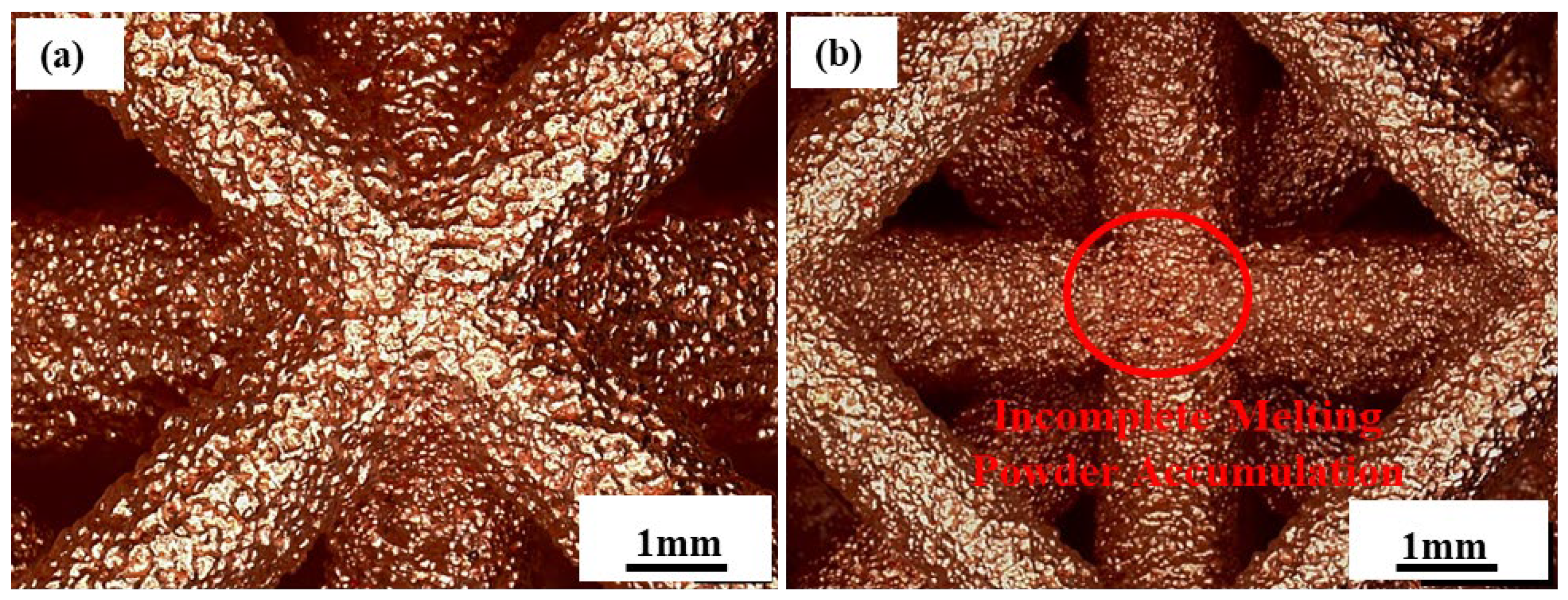
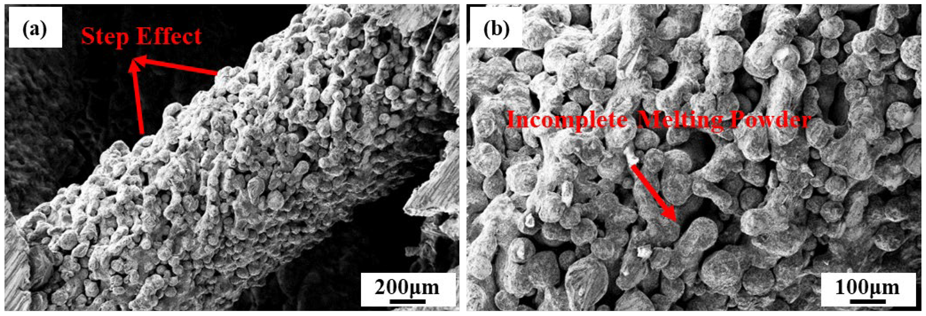
3.1. Overall Quality Analysis of Samples

The pure copper OCTET lattice structure was formed using the SEBM technology, resulting in a stable process without splashing or powder blowout. Figure 2 shows the pure copper OCTET lattice structure sample produced by SEBM. The macrostructure of the sample aligned well with the design specifications, demonstrating good connectivity. Notably, there were no disconnections, cracks, incomplete prints, or other defects at the joints or the connection between the lattice structure and the sandwich plate, ensuring that these defects did not affect the performance of the lattice structure. Additionally, the powder in the pores of the samples with cell sizes of 7.5 mm and 10 mm was easy to clean, indicating that the pore and relative density designs were reasonable. However, for the samples with a cell size of 5 mm, the internal pores were smaller, especially for those with strut diameters of 1.2 mm and 1.4 mm, making the internal powder difficult to clean.
The internal powder was difficult to clean because the gaps between the struts were too small. The length–diameter ratio of the lattice structure, shown in Table 3, should be considered. To avoid the issue of hard-to-clean powder within the lattice, the aspect ratio should be maintained above 2.95 when designing the SEBM-formed pure copper OCTET lattice structure. Additionally, the forming ability of a pure copper strut must be comprehensively considered in the design. The results in Table 3 indicate that as the cell size increases, the length–diameter ratio error of the lattice structure decreases gradually.
Lattice structures formed by SEBM are prone to microdefects, such as strut corrugation, size variations, and small pore defects [29]. The formation of a lattice structure with a 1.0 mm strut diameter and a 7.5 mm cell size was observed using an ultra-depth field stereomicroscope. The outer column surface (Figure 3a) was uneven, while the inner column surface (Figure 3b) exhibited significant stickiness, step phenomena, and column rippling defects. Due to the excellent heat transfer properties of pure copper and the unique heat transfer mode in the SEBM process, the surface of the pure copper lattice structure tends to accumulate sticky powder. This powder accumulation at the lattice strut connections is primarily due to longer printing times, leading to greater energy accumulation and more severe powder adhesion, which in turn causes changes in the size of the lattice structure.
The sticky powder phenomenon is common in metal bed additive manufacturing processes. It occurs when powder in the heat-affected zone is not completely melted and adheres to the surface of the formed part. The main reasons are as follows. Firstly, electron beam selective melting technology features rapid solidification, causing a significant temperature difference between the solidification area and the surrounding powder. This results in thermal diffusion, leading to higher energy accumulation at the edge of the forming area. The small forming area of the lattice strut is covered with metal powder, which has poorer thermal conductivity than the strut. This causes heat to accumulate in the molten pool during the forming process, resulting in partial melting and adhesion of the surrounding powder. Additionally, the excellent thermal conductivity of pure copper quickly transfers heat to the heat-affected zone, making it larger than in other materials and exacerbating the sticky powder phenomenon. Pure copper’s low melting point (1083 °C) and high thermal conductivity increase the tendency for sintering during the forming process. Additionally, the small internal pores in samples 5–1.2 and 5–1.4 concentrated energy, intensifying sintering. This made the sintered powder difficult to remove, increasing surface corrugation and size variation of the strut, which affected the mechanical properties of the lattice structure. When designing pure copper lattice structures, considerations for powder adhesion and sintering are crucial to avoid difficulties in cleaning internal powder, and further polishing treatment is necessary [30].
To further examine the surface morphology of the strut, a scanning electron microscope was used to observe the surface of the pure copper lattice structure formed by SEBM, as shown in Figure 4. The figure shows no cracks, deformation, or fractures in the single-cell struts, indicating a stable forming process. This observation confirms that the serious sticky powder and incomplete melting on the surface of the sample are the primary causes of the step effect and size variation in the strut.
Figure 5 shows the cross-section of a lattice structure strut. The image reveals that the sample surface was sintered with adhesive powder and contained holes, leading to a decrease in material density. This was the major reason for the deviation between the actual and designed relative densities. Additionally, microcracks and internal holes in the strut increased the likelihood of crack propagation, resulting in bending and deformation along the crack direction.
Figure 6 compares the theoretical relative density (TRD) and the actual relative density (ARD) of the lattice structure. The figure shows that as the cell size increased, the error between the TRD and ARD decreased. This occurred because with a smaller relative density, the energy input during the forming process is lower, resulting in a smaller molten pool size and a lower temperature difference. Larger cell sizes lead to larger heat dissipation areas in low-energy printing areas, reducing the deviation between the actual and designed relative densities. When designing the relative density of a lattice structure, it is important to consider not only the step effect and high relative density caused by powder adhesion in the SEBM technology, but also the influence of the structure on these factors. Additionally, the actual relative density of the sample was calculated using the density formula, with density measured with a densitometer and mass—with an electronic balance. Measurement errors and sample defects could also contribute to lower density.

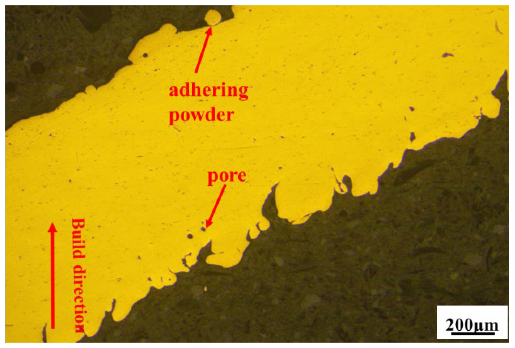
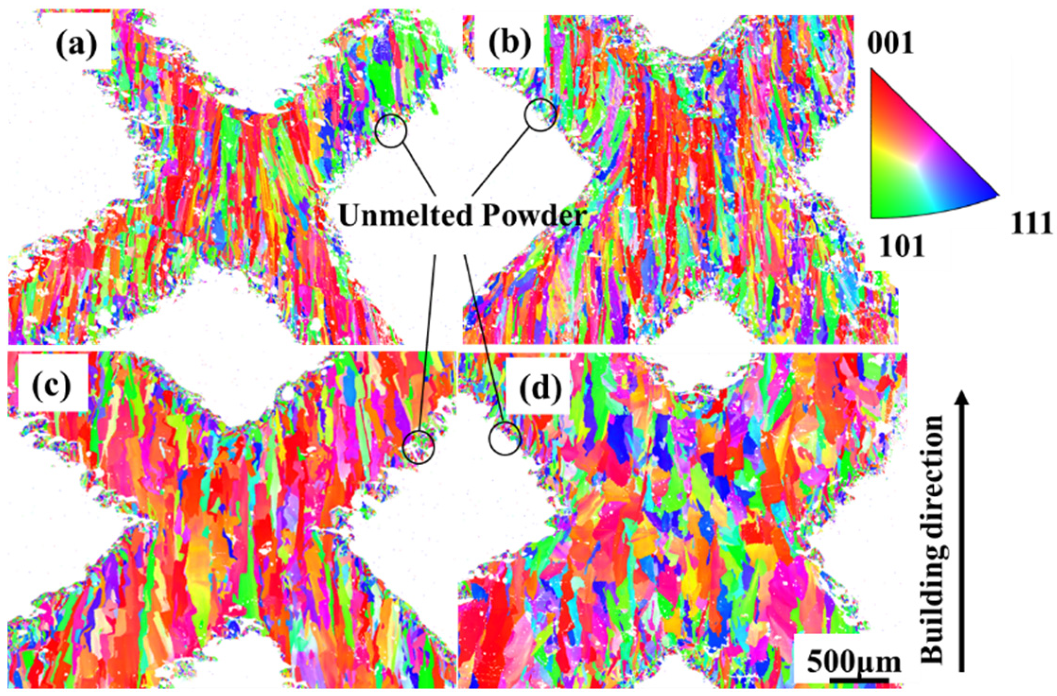
3.2. Microstructure Analysis

Figure 7 shows the EBSD images of a pure copper lattice structure with a 7.5 mm cell size and varying strut diameters. The structure primarily consisted of slender columnar crystals whose growth direction aligned with the forming direction and was parallel to the thermal gradient, exhibiting pronounced epitaxial growth. As the strut diameter increased, the energy input increased, the solidification rate decreased, and the extent of epitaxial grain growth diminished.
During SEBM sample formation, the microstructure displayed strong directional solidification and epitaxial growth characteristics, manifested as multiscale columnar crystals. The rapid solidification rate and high temperature gradient provided favorable thermodynamic conditions for columnar crystal growth. When the first layer melted, some of the previous layers remelted, extending the epitaxial growth time. The high temperature gradient at the solid–liquid interface reduced the degree of subcooling (the difference between the actual melt temperature and the equilibrium liquid phase temperature), inhibited spontaneous nucleation at the interface, and promoted the epitaxial growth of columnar crystals. Due to the unique thermal history of the SEBM process, the grains grew in multiple sedimentary layers. The microstructure of the samples consisted of columnar grains oriented along the construction direction, exhibiting anisotropic characteristics with a predominance of preferentially oriented grains. Additionally, issues such as adhesive powder and incomplete melting of the powder were observed in the SEBM-formed pure copper samples.

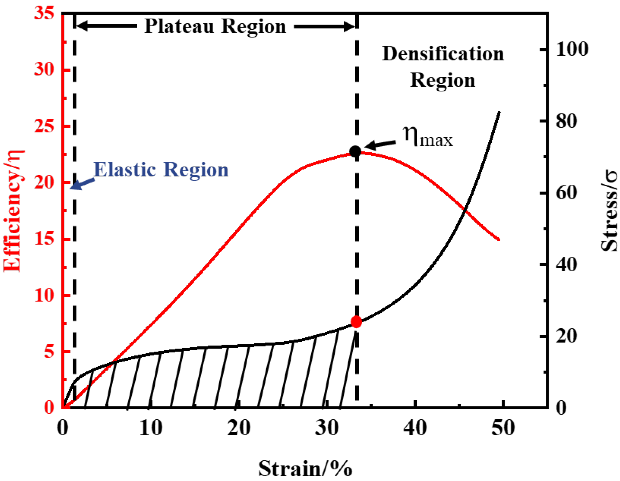
3.3. Compression Properties

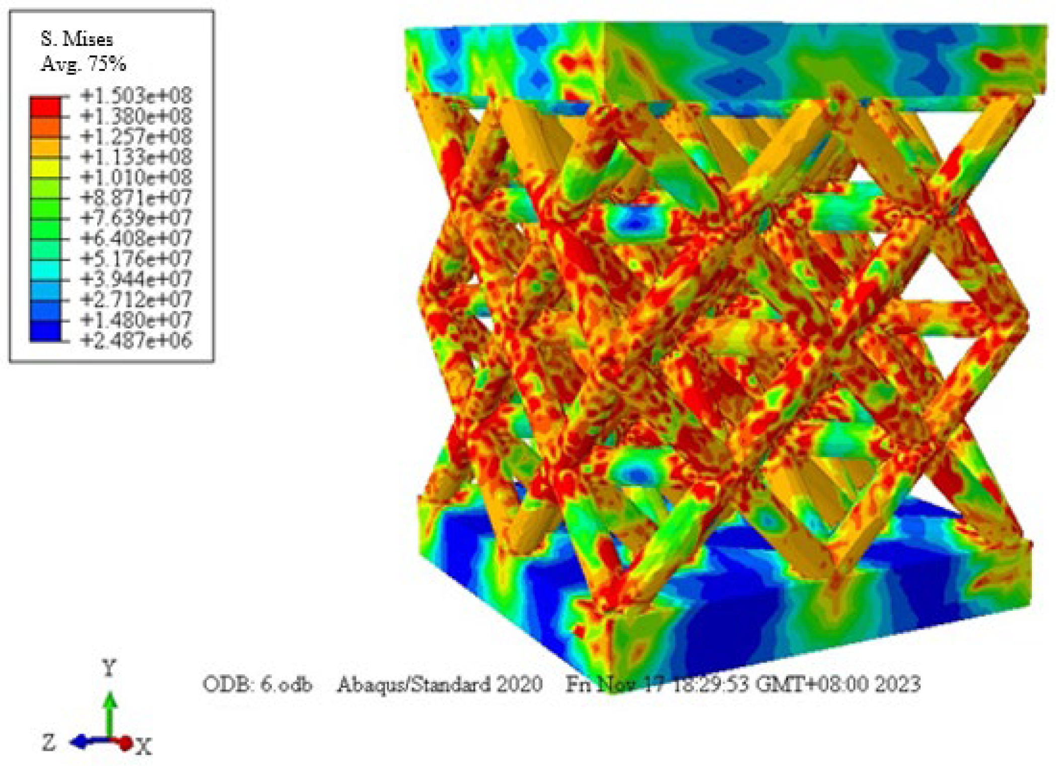
3.3.1. Numerical Study

The ABAQUS 2022 software was used to simulate the quasistatic compression behavior of an octahedral lattice sandwich structure. The material properties were set as follows: density of 8.92 g/cm3, Young’s modulus of 118 GPa, yield strength of 133 MPa, and Poisson’s ratio of 0.34 [31,32]. Figure 8 displays the stress distribution in the octahedral lattice structure. The figure reveals significant stress concentration at the lattice nodes. This was primarily because the nodes exhibited the highest plastic bending resistance during compression, leading to the formation of plastic hinges at these points rather than at regions with lower stress. Additionally, the figure shows a lattice structure with a 5 mm cell size and a 1.0 mm strut diameter. During compression, stress was concentrated in the middle region of the structure, while the regions near the upper and lower solid plates exhibited lower stress values. Consequently, deformation initiated in the middle region during compression.

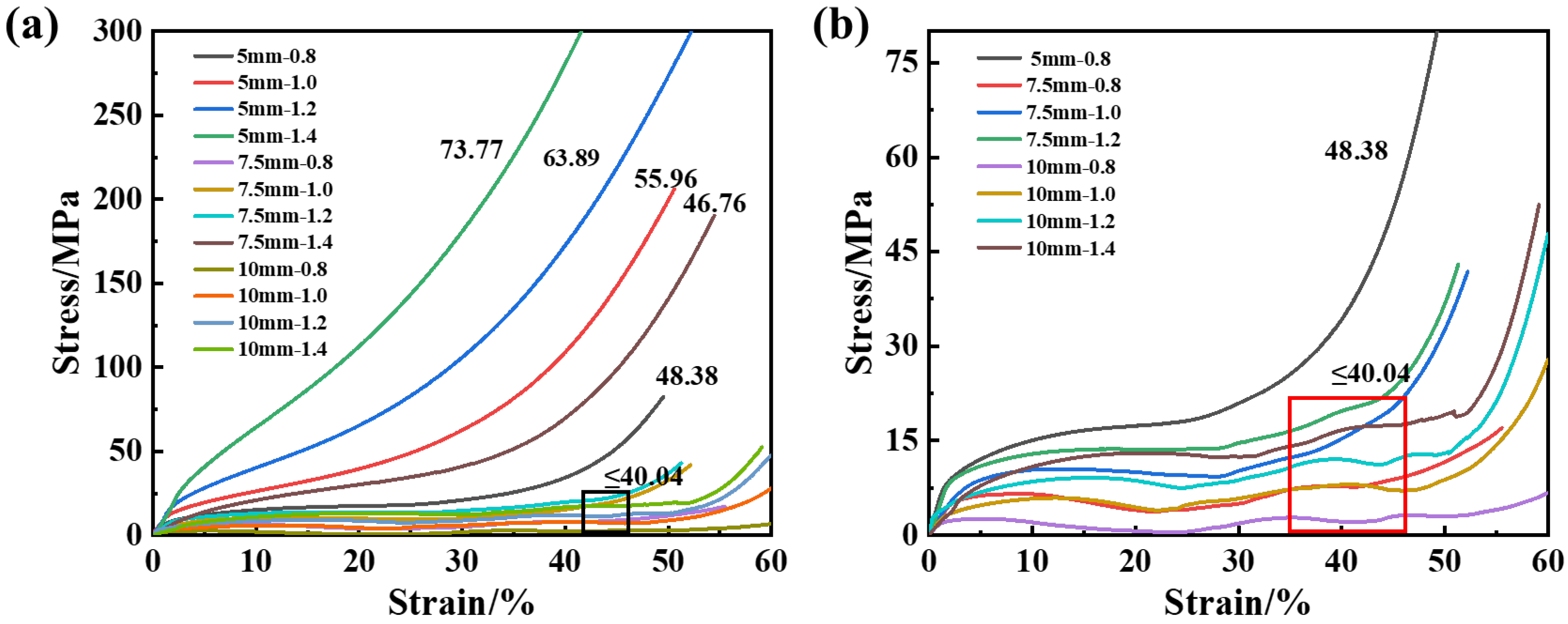
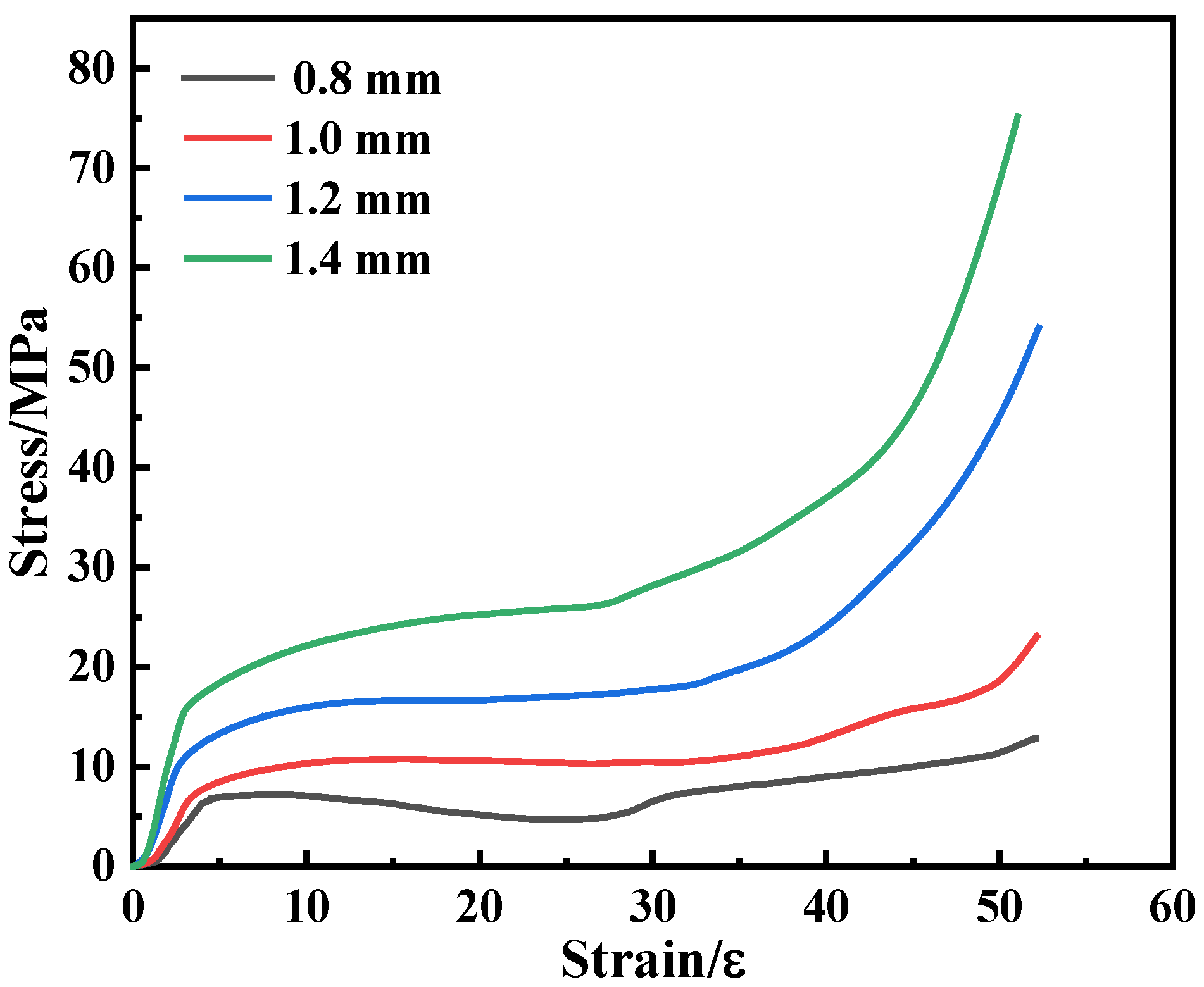
3.3.2. Experimental Study

OCTET is a tension-dominated lattice structure, and its stress–strain curve should exhibit a linear elastic stage, a plastic deformation stage with stress oscillations, and a densification stage. Figure 9a presents the stress–strain curves for SEBM-formed pure copper OCTET lattice structures with varying cell parameters. It is evident from the figure that not all samples displayed the plastic deformation stage with stress oscillations. For clarity, Figure 9b provides a statistical analysis of the stress–strain curves for the lattice samples with relatively low density. This analysis shows that while all lattice structures exhibited linear deformation in the elastic stage, there were significant variations in the stress–strain curves during the plastic deformation stage. When the relative density was at least 40.04%, the stress–strain curve demonstrated an approximately linear positive hardening. In contrast, when the relative density was below 40.04%, stress oscillations were observed, characteristic of typical tensile lattice structures. The initial phase showed a linear elastic deformation, with a steeper curve indicating a higher elastic modulus. This was followed by the plastic deformation stage, where stress increased nonlinearly and shear deformation occurred, reducing the curve’s slope. As deformation progressed, stress began to decline, with the maximum stress representing the compressive strength. The number of oscillation peaks corresponded to the number of layers in the lattice structure, with peaks indicating ordered folding and collapse. A longer oscillation phase suggested better ductility. As deformation continued, the lattice structure eventually broke down, leading to densification and a rapid increase in stress.
According to international standard ISO 13314:2011 [33] for testing compressive properties of porous structures (applicable to samples with porosity below 50%), the yield strength is defined as the stress corresponding to a plastic deformation of 0.2%. The elastic modulus is determined by the slope of the linear phase of the stress–strain curve. For curves exhibiting oscillations, the first peak in stress is taken as the compressive strength. For curves without oscillating peaks, the compressive strength is represented by the average stress between the initial strain of plastic deformation and the initial strain of densification (i.e., the platform stress). The main formula is expressed as follows [34,35]:
σ p = ε y ε d σ ( ε ) d ε ε d ε y ,
where σp is the compressive strength (MPa), εd is the densification initiation variable (%), and εy is the initial strain of plastic deformation (%).
Energy absorption capacity (EA, MJ/m3) is the area under the stress–strain curve calculated as follows:
EA = 0 ε a σ ε d ε
The densification initiation site η can be determined by the energy absorption efficiency, which is a key parameter in evaluating the energy absorption characteristics of the buffer structure. A higher energy absorption efficiency indicates a better energy absorption capacity of the structure. Energy absorption efficiency is defined as the ratio of the energy absorbed to the stress σ(ε) generated at any strain ε from Equation (4):
η = 0 ε a σ ( ε ) d ε σ ( ε )
The densification strain (the maximum point of the curve η) is derived from Equation (4):
d η d ε a ε d = ε a = 0
Taking the 5–0.8 mm sample as an example, its energy absorption efficiency and densification site are illustrated in Figure 10. In the figure, ηmax represents the maximum energy absorption efficiency and the corresponding strain value εd denotes the strain at which densification begins, reflecting the dimensional shrinkage rate of the lattice structure. The total energy absorbed is calculated as the area under the stress–strain curve up to this strain. Similar analyses were performed to determine the densification starting points and energy absorption efficiencies for other lattice structures. However, for the samples with lattice structures of 5–1.2 mm and 5–1.4 mm, the relatively high relative density meant that this method of calculation was not applicable.
Table 4 presents the compressive strength, densification strain points, energy absorption capacity, and energy absorption efficiency for lattice structures with varying cell parameters. The table indicates that for specimens with cell sizes of 5 mm and 10 mm, the densification point increased with the strut diameter and, consequently, with the relative density. This trend was consistent because the stress–strain curve behavior was similar for these specimens: those with a 5 mm cell size exhibited a monotonically increasing stress–strain response, while those with a 10 mm cell size showed oscillatory instability. For the 7.5 mm cell size sample, the densification point initially increased and then decreased with increasing strut diameter. The total energy absorption also gradually increased with the strut diameter, reflecting the relationship between relative density and compression response. When the relative density was at least 40.04%, the macrostrain compression response stabilized. Below this density, the structure tended to exhibit oscillatory instability, while above this density, the stress–strain response became monotonically increasing, providing a stable stress platform. This stability indicated a higher deformation and energy absorption capacity. Yang et al. [22] reported an energy absorption of 0.19 MJ/m3 per unit volume for a reentrant pure copper lattice structure with a relative density of 20.80%. In this study, a lattice structure with a relative density of 21.16% achieved an energy absorption of 0.37 MJ/m3, slightly higher than that of the previous study. The maximum energy absorption per unit volume recorded was 15.00 MJ/m3. Additionally, the densification site (size shrinkage rate) of the lattice structures ranged from 23.96% to 51.68%, meaning the size deformation before densification was between 23.96% and 51.68% of the original sample. Among these, the sample with a 10–1.4 mm cell size exhibited the largest deformation range, with a maximum shrinkage of 51.68% and a weight loss of 67.35%. In comparison, Ramirez et al. [21] reported a 12% size shrinkage for a pure copper foam prepared using the SEBM technology, indicating that the lattice structure exhibits a significantly higher shrinkage than the foam structure.

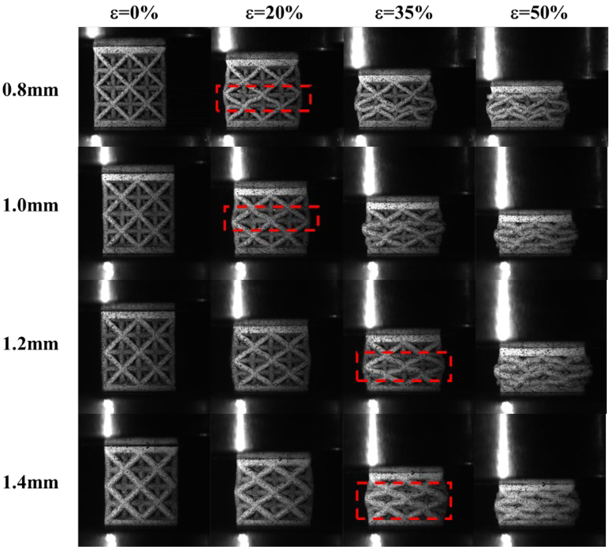
3.3.3. Effect of the Strut Diameter on the Compression Failure Mode

Figure 11 illustrates the compression failure modes of the lattice sandwich structure for samples with a cell size of 7.5 mm and varying strut diameters (0.8 mm, 1.0 mm, 1.2 mm, and 1.4 mm). As shown in the figure, when the strut diameter was 0.8 mm, deformation initially occurred in one layer of the sample. As the strain increased, this deformation propagated to the adjacent layers, resulting in a distinct layer-by-layer failure mode. This behavior corresponded to the stress–strain curve: after reaching the limit of elastic deformation, the first peak appeared, followed by deformation in a particular layer and a subsequent decrease in stress. With further strut deformation, a second peak was observed due to accumulation. Continued compression led to densification of the entire sample after the first two layers had failed, which was reflected as a linear increase in the stress–strain curve following these peaks. The observed buckling-dominated failure (Figure 11) aligned with the inherent instability of tension-dominated lattice structures under compressive loading. While the theoretical Euler buckling load provides a fundamental framework for understanding strut instability, the experimental compressive strength was reduced by microstructural defects such as surface corrugation, internal porosity, and sintered powder (Figure 4 and Figure 5), which acted as stress concentrators and promoted premature buckling. Additionally, the anisotropic mechanical response induced by the SEBM process—characterized by elongated columnar grains aligned parallel to the build direction (Figure 7)—may further lower buckling resistance due to inhomogeneous plastic deformation.
As the strut diameter increased, the failure mode of the lattice structure evolved from single-layer failure to concentrated failure. The plastic deformation stage of the stress–strain curve transitioned from a shock-like response to a more gradual curve. When the strut diameter reached 1.4 mm, the stress–strain curve approximated that of a densified material, exhibiting a linear increase. Deformation became more uniformly distributed across the sample but remained concentrated in the central region. At that stage, the struts primarily acted as resistance sites to further deformation, facilitating the onset of densification. The transition to stable plastic collapse at larger strut diameters (e.g., 1.2–1.4 mm) suggested that the increased strut diameter mitigated defect sensitivity by reducing the relative impact of surface imperfections and internal voids, thereby enhancing the load-bearing capacity. These findings are consistent with those reported by Yang et al. [22].
Analysis of the compression process for lattice structures with a cell size of 7.5 mm and varying strut diameters (0.8, 1.0, 1.2, and 1.4 mm) revealed that axial compression buckling and plastic yield deformation occurred perpendicular to the compression load. For a strut diameter of 0.8 mm, the connecting struts exhibited significant flexibility. As the load increased, plastic hinges developed at the strut nodes, leading to deformation and a rapid decrease in the lattice structure’s load-bearing capacity. When the deformation of one layer of struts reached the diameter of the struts, deformation in the subsequent layer began, resulting in a transition from localized failure to overall failure, characterized by layer-by-layer collapse. As the strut diameter increased, the load-bearing capacity improved, and the deformation mode of the lattice structure changed. For a strut diameter of 1.0 mm, axial compression initially caused buckling deformation, which then transitioned to a stable plastic deformation mode that maintained a stable load-bearing platform. With further increases in strut diameter, the lattice exhibited a stable yield deformation mode during compression, with struts undergoing extensive plastic deformation. This behavior was attributed to the decreased length–diameter ratio and the increased relative density with larger strut diameters. The shorter distance between strut nodes and the interaction between adjacent plastic hinges created a continuous plastic deformation zone throughout the lattice. Deformation predominantly occurred in the central region, aligning with the stress analysis results.

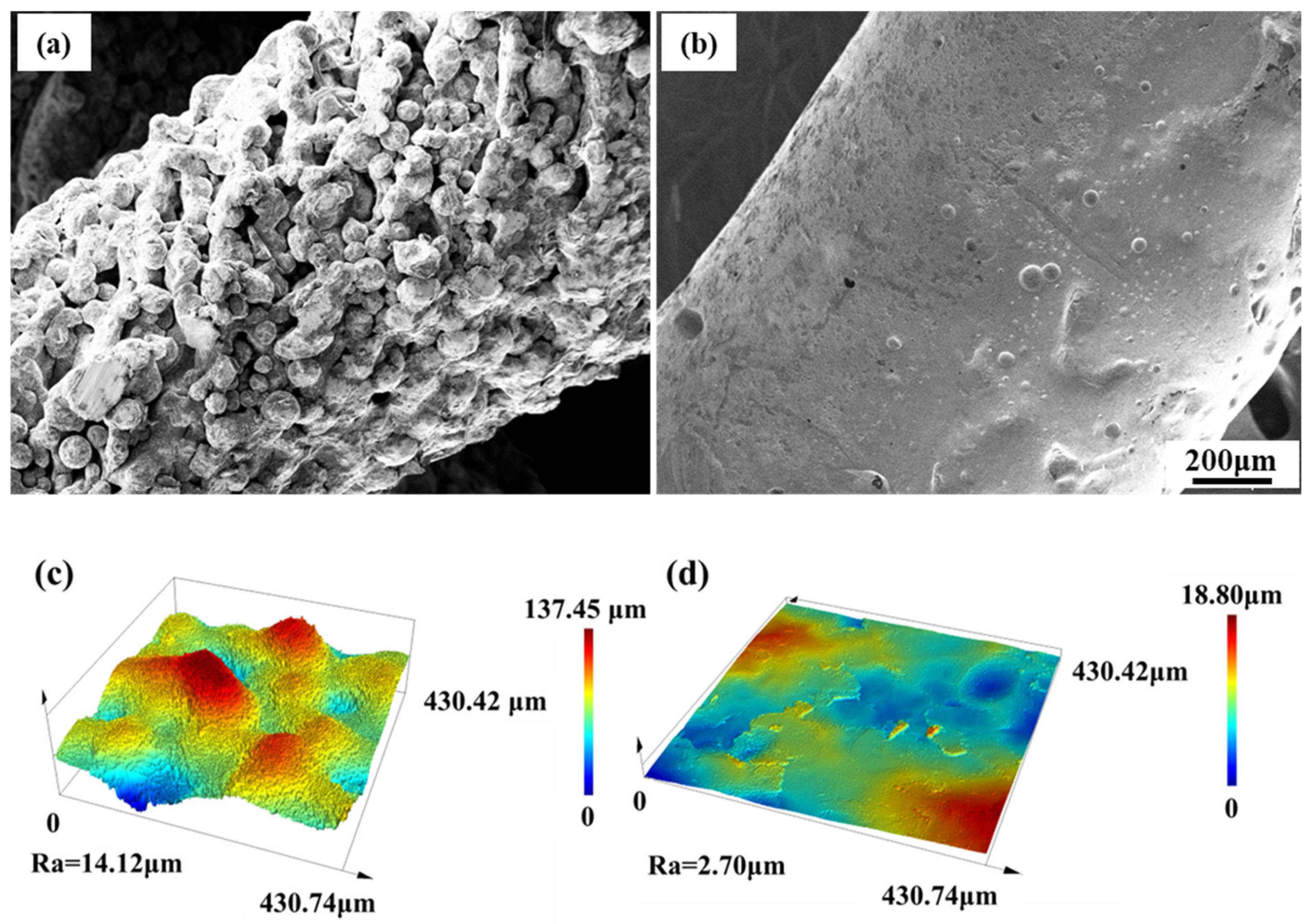
3.4. Surface Morphology and Compression Properties After Surface Treatment

3.4.1. Surface Morphology

Surface adhesion powder affects material properties. To address this, a magnetic polishing technology was employed after initial surface polishing. This process involves controlling the rapid rotation of magnetic needles through a magnetic field, which induces friction within the sample and achieves effective polishing by removing surface adhesion and sintered powder. Post-magnetic polishing, the adhesive powder on the sample’s surface was largely eliminated. This technique effectively removes adhesive powder, thereby preventing any adverse effects on material properties. Additionally, the magnetic polishing process restored the struts to their cylindrical shape, significantly reducing strut corrugation and improving surface topography. The removal of strut waviness and adhesive powder enhanced forming accuracy, though some hole defects remained, as illustrated in Figure 12a,b. Laser confocal microscopy was used to measure surface roughness, with the results shown in Figure 12c,d. The average height difference, represented by the Ra value, was used to characterize surface roughness. The initial Ra value of the sample was 14.12 μm, which decreased to 2.70 μm after magnetic polishing, indicating a significant improvement in surface roughness.

3.4.2. Compression Properties

Surface roughness impacts the mechanical properties of materials. Figure 13 presents the compressive properties of polished samples. The figure illustrates that as the strut diameter increased, the stress–strain curve of the lattice structure transitioned from exhibiting noticeable stress oscillations (for a strut diameter of 0.8 mm) to a stable stress plateau (for strut diameters of 1.0, 1.2, and 1.4 mm). Table 5 provides the calculated relative density and mechanical properties of the polished samples. It shows that both the yield strength and the elastic modulus of the lattice structure increased with strut diameter. Notably, compared to the pre-polishing values, the relative density of the samples decreased after polishing.
Compressive strength and densification strain are key indicators of the energy absorption characteristics of lattice structures. Figure 14 shows the fitted relationship between stress–strain behavior, energy absorption efficiency, and strain for the samples with varying strut diameters, with the results statistically analyzed in Table 6. The findings indicate that as the strut diameter increased, the compressive strength of the lattice structure increased. Additionally, the strain, stress, and energy absorption at the densification strain site all increased with larger strut diameters. However, the energy absorption efficiency slightly decreased as the strut diameter grew, suggesting that the energy absorption capacity was not fully optimized with increasing strut diameter.
Research on the octahedral lattice structure has been conducted by various researchers. Dong et al. [36] derived the relationship between compressive strength and relative density for the octahedral lattice structure:
σ pl = 1 3 ρ rel σ ys ,
where σys is the yield strength of solid copper (133 MPa) [31].
The platform stress of the polished specimens was compared with the theoretical platform stress, with the results summarized in Table 7. As shown in the table, for the strut diameters of 0.8 mm and 1.0 mm, the platform stress of the lattice structure was lower than the theoretical platform stress, indicating that internal hole defects reduced the mechanical properties of the lattice structure. Conversely, for the strut diameters of 1.2 mm and 1.4 mm, the platform stress of the lattice structure exceeded the theoretical platform stress, suggesting that while internal defects reduced the mechanical properties, the increased strut diameter improved the overall properties of the lattice structure. Furthermore, for the strut diameters greater than 1.2 mm, the compressive properties of the lattice structure showed a significant improvement.
Specific energy absorption capacity refers to the energy absorbed by a material per unit of macroscopic density, while specific strength is the strength divided by the macroscopic density. Both specific energy absorption capacity and specific strength are critical indicators of material performance. Figure 15 compares the specific energy absorption capacity and the specific strength of the samples before and after polishing. The figure shows that the specific energy absorption capacity of the samples remained largely unchanged after polishing, indicating that the adhesive powder had minimal impact on the energy absorption capacity. In contrast, polishing improved the specific strength of the specimens with strut diameters of 0.8 mm and 1.0 mm, but reduced the specific strength of the specimens with a 1.4 mm strut diameter. For the samples with larger strut diameters, polishing reduced surface microdefects, which affected the specific strength primarily through changes in strut diameter. Consequently, as the strut diameter increased, the effect of microdefects on the specific strength of the lattice structure diminished.

4. Conclusion

This study investigated the pure copper OCTET lattice structure formed by SEBM, focusing on how different cell sizes and strut diameters affect its forming characteristics, microstructure, failure modes, mechanical properties, and energy absorption characteristics. The lattice structure was magnetically polished to remove adhesive powder, and the impact of this polishing on lattice properties was examined. The main conclusions are as follows:
(1) The macrostructure of the pure copper OCTET lattice formed by SEBM closely matched the designed structure, with good connectivity, indicating the effectiveness of the SEBM technology in producing pure copper lattice structures. The actual relative density of the lattice was higher than the theoretical density due to microdefects such as surface adhesive powder and internal holes. SEBM-formed pure copper lattices exhibited coarse columnar crystals aligned parallel to the construction direction. The size of these columnar crystals was influenced by the cooling rate and solidification time, increasing with strut diameter.
(2) The macrostrain compression response of the SEBM-formed copper OCTET lattice changed when the relative density reached 40.04%. For relative densities below 40.04%, compressive deformation resulted in a layer-by-layer collapse, with the stress–strain curve showing oscillatory behavior. For relative densities equal to or greater than 40.04%, the response stabilized, resulting in uniform deformation and a stress–strain curve that was either flat or exhibited hardening behavior.
(3) The densification strain sites for the SEBM-formed pure copper lattice structures ranged from 23.96% to 51.68%, with the largest deformation observed in the sample with a 10–1.4 mm cell size, reaching 51.68%. The maximum energy absorption per unit of volume was 15.00 MJ/m3. The specific energy absorption capacity increased with strut diameter, decreased slightly with increasing cell size, and then increased again. The specific surface area decreased with increasing strut diameter.
(4) Polishing the specimen with a cell size of 7.5 mm significantly reduced surface adhesion powder, decreasing surface roughness from 14.12 μm to 2.70 μm and reducing the strut size deviation. Internal defects could reduce compressive strength, but the performance of the lattice was enhanced by the upper and lower interlayers. For the strut diameters greater than 1.2 mm, these interlayers significantly improved compressive performance. Microdefects such as strut ripples and adhesive powder weakened the specific strength of the lattices with smaller strut diameters (0.8 and 1.0 mm), while for the lattices with larger strut diameters (1.2 mm), the specific strength was primarily influenced by the strut diameter.

Author Contributions

Conceptualization, X.Y.; data curation, F.S. and X.X.; formal analysis, Z.Z. and X.X.; funding acquisition, H.Q.; investigation, Z.Z. and F.S.; supervision, C.D.; writing—original draft preparation, X.Y.; writing—review and editing, H.Q. and C.D. All authors have read and agreed to the published version of the manuscript.

Funding

This research was funded by the National Key R&D Program of China (2024YFB4608500), National Natural Science Foundation of China (No. 52475493), Key Scientific Research Project of Hangzhou City (2023SZD0072).

Institutional Review Board Statement

Not applicable.

Informed Consent Statement

Not applicable.

Data Availability Statement

Data available upon request due to restrictions.

Conflicts of Interest

The authors declare no conflicts of interest.

References

  1. Thomas, A.; Fribourg, G.; Blandin, J.-J.; Lhuissier, P.; Dendievel, R.; Martin, G. Effect of the build orientation on mechanical and electrical properties of pure Cu fabricated by E-PBF. Addit. Manuf. 2021, 48, 102393. [Google Scholar] [CrossRef]
  2. Guschlbauer, R.; Momeni, S.; Osmanlic, F.; Körner, C. Process development of 99.95% pure copper processed via selective electron beam melting and its mechanical and physical properties. Mater. Charact. 2018, 143, 163–170. [Google Scholar] [CrossRef]
  3. Ledford, C.; Rock, C.; Carriere, P.; Frigola, P.; Gamzina, D.; Horn, T. Characteristics and Processing of Hydrogen-Treated Copper Powders for EB-PBF Additive Manufacturing. Appl. Sci. 2019, 9, 3993. [Google Scholar] [CrossRef]
  4. Selivanov, V.V.; Silnikov, M.V.; Markov, V.A.; Popov, Y.V.; Pusev, V.I. Using highly porous aluminum alloys and honeycomb structures in spacecraft landing gear. Acta Astronaut. 2021, 180, 105–109. [Google Scholar] [CrossRef]
  5. Nanda, S.; Gupta, A.; Manthiram, A. Anode-Free Full Cells: A Pathway to High-Energy Density Lithium-Metal Batteries. Adv. Energy Mater. 2021, 11, 2000804. [Google Scholar] [CrossRef]
  6. Zhang, G.; Li, L.; Zhao, Z.-J.; Wang, T.; Gong, J. Electrochemical Approaches to CO2 Conversion on Copper-Based Catalysts. Acc. Mater. Res. 2023, 4, 212–222. [Google Scholar] [CrossRef]
  7. Gibson, I.; Rosen, D.W.; Stucker, B.; Khorasani, M. Additive Manufacturing Technologies; Springer: Cham, Switzerland, 2021. [Google Scholar]
  8. Gibson, I.; Rosen, D.; Stucker, B.; Khorasani, M. Design for additive manufacturing. In Additive Manufacturing Technologies; Springer: Cham, Switzerland, 2021; pp. 555–607. [Google Scholar]
  9. Manyika, J.; Chui, M.; Bughin, J.; Dobbs, R.; Bisson, P.; Marrs, A. Disruptive Technologies: Advances That Will Transform Life, Business, and the Global Economy; McKinsey Global Institute: San Francisco, CA, USA, 2013. [Google Scholar]
  10. Gibson, I.; Rosen, D.; Stucker, B.; Khorasani, M. Development of additive manufacturing technology. In Additive Manufacturing Technologies; Springer: Cham, Switzerland, 2021; pp. 23–51. [Google Scholar]
  11. Liu, G.; Zhang, X.; Chen, X.; He, Y.; Cheng, L.; Huo, M.; Yin, J.; Hao, F.; Chen, S.; Wang, P.; et al. Additive manufacturing of structural materials. Mater. Sci. Eng. R Rep. 2021, 145, 100596. [Google Scholar] [CrossRef]
  12. Körner, C. Additive manufacturing of metallic components by selective electron beam melting—A review. Int. Mater. Rev. 2016, 61, 361–377. [Google Scholar] [CrossRef]
  13. Eiji, H.; Yuji, S.; Tomoki, S.; Koji, T.; Masahiro, T. Development of SLM process using 200 W blue diode laser for pure copper additive manufacturing of high density structure. J. Laser Appl. 2021, 33, 12008. [Google Scholar]
  14. Surajdinkar, J.; Loucaraphaël, G.; Yannis, K.; Brecht, V.H.; Kim, V. Laser-based powder bed fusion additive manufacturing of pure copper. Addit. Manuf. 2021, 42, 101990. [Google Scholar]
  15. Colopi, M.; Caprio, L.; Demir, A.; Previtali, B. Selective laser melting of pure Cu with a 1 kW single mode fiber laser. Procedia Cirp 2018, 74, 59–63. [Google Scholar] [CrossRef]
  16. Shinichiro, M.; Masahiro, T.; Koji, T.; Asano, K.; Asuka, K.; Funada, Y.; Sakon, Y. Metal powder bed fusion additive manufacturing with 100W blue diode laser. In International Congress on Applications of Lasers & Electro-Optics; Laser Institute of America: Orlando, FL, USA, 2017; p. 130. [Google Scholar]
  17. Singh, A.; Caprio, L.; Previtali, B.; Demir, A.G. Processability of pure Cu by LPBF using a ns-pulsed green fiber laser. Opt. Laser Technol. 2022, 154, 108310. [Google Scholar] [CrossRef]
  18. Lodes, M.A.; Guschlbauer, R.; Koerner, C. Process development for the manufacturing of 99.94% pure copper via selective electron beam melting. Mater. Lett. 2015, 143, 298–301. [Google Scholar] [CrossRef]
  19. Megahed, S.; Fischer, F.; Nell, M.; Forsmark, J.; Leonardi, F.; Zhu, L.; Hameyer, K.; Schleifenbaum, J.H. Manufacturing of Pure Copper with Electron Beam Melting and the Effect of Thermal and Abrasive Post-Processing on Microstructure and Electric Conductivity. Materials 2022, 16, 73. [Google Scholar] [CrossRef]
  20. Frigola, P.; Harrysson, O.L.; Horn, T.; West, H.; Aman, R.; Rigsbee, J.; Ramirez, D.; Murr, L.; Medina, F.; Wicker, R.; et al. Fabricating copper components. Adv. Mater. Process 2014, 172, 20–24. [Google Scholar]
  21. Ramirez, D.A.; Murr, L.E.; Li, S.; Tian, Y.; Martinez, E.; Martinez, J.; Machado, B.; Gaytan, S.; Medina, F.; Wicker, R. Open-cellular copper structures fabricated by additive manufacturing using electron beam melting. Mater. Sci. Eng. A 2011, 528, 5379–5386. [Google Scholar] [CrossRef]
  22. Yang, L.; Harrysson, O.; West, H.; Cormier, D. Design and Characterization of Orthotropic Re-Entrant Auxetic Structures Made via EBM Using Ti6Al4V and Pure Copper. In Proceedings of the 2011 International Solid Freeform Fabrication Symposium, Austin, TX, USA, 8–10 August 2011. [Google Scholar]
  23. Xueyan, C.; Huifeng, T. An effective length model for octet lattice. Int. J. Mech. Sci. 2018, 140, 279–287. [Google Scholar]
  24. Tancogne-Dejean, T.; Spierings, A.B.; Mohr, D. Additively-manufactured metallic micro-lattice materials for high specific energy absorption under static and dynamic loading. Acta Mater. 2016, 116, 14–28. [Google Scholar] [CrossRef]
  25. Peng, Z.; Deqing, H.; Yongfu, Z.; Zhang, H.; Chen, W. Microstructure and Properties of Hollow Octet Nickel Lattice Materials. Materials 2022, 15, 8417. [Google Scholar] [CrossRef]
  26. O’Masta, M.R.; Dong, L.; St-Pierre, L.; Wadley, H.; Deshpande, V.S. The fracture toughness of octet-truss lattices. J. Mech. Phys. Solids 2017, 98, 271–289. [Google Scholar] [CrossRef]
  27. Wang, N.; Meenashisundaram, G.K.; Chang, S.; Fuh, J.Y.H.; Dheen, S.T.; Kumar, A.S. A comparative investigation on the mechanical properties and cytotoxicity of Cubic, Octet, and TPMS gyroid structures fabricated by selective laser melting of stainless steel 316L. J. Mech. Behav. Biomed. Mater. 2022, 129, 105151. [Google Scholar] [CrossRef] [PubMed]
  28. ASTM B170-99(2020); Standard Specification for Oxygen-Free Electrolytic Copper—Refinery Shapes. ASTM International: West Conshohocken, PA, USA, 2020.
  29. Liu, L.; Kamm, P.; García-Moreno, F.; Banhart, J.; Pasini, D. Elastic and failure response of imperfect three-dimensional metallic lattices: The role of geometric defects induced by Selective Laser Melting. J. Mech. Phys. Solids 2017, 107, 160–184. [Google Scholar] [CrossRef]
  30. Manuela, G.; Luca, I. A literature review of powder-based electron beam melting focusing on numerical simulations. Addit. Manuf. 2018, 19, 1–20. [Google Scholar]
  31. Wendy, G.; Julia, G. Ultra-strong architected Cu meso-lattices. Extrem. Mech. Lett. 2015, 2, 7–14. [Google Scholar] [CrossRef]
  32. Shoudao, Q.; Zesheng, Y.; Ruicong, G.; Yao, J.; Jing Tao, W. Fracture toughness anisotropy of ultrafine-grained pure copper processed by equal channel angular pressing. Mater. Sci. Eng. A 2020, 782, 139260. [Google Scholar]
  33. ISO 13314:2011; Mechanical testing of metals-Ductility testing-Compression test for porous and cellular metals. ISO International Organization for Standardization: Geneva, Switzerland, 2011.
  34. Sharma, D.; Hiremath, S.S. Bio-inspired repeatable lattice structures for energy absorption: Experimental and finite element study. Compos. Struct. 2022, 283, 115102. [Google Scholar] [CrossRef]
  35. Jianhu, S.; Guoxing, L.; Dong, R. Compressive behaviour of closed-cell aluminium foams at high strain rates. Compos. Part B Eng. 2010, 41, 678–685. [Google Scholar]
  36. Dong, L.; Deshpande, V.; Wadley, H. Mechanical response of Ti–6Al–4V octet-truss lattice structures. Int. J. Solids Struct. 2015, 60, 107–124. [Google Scholar] [CrossRef]
Figure 1. OCTET single cell and lattice structure model.
Coatings 15 00348 g001
Figure 2. SEBM-formed pure copper lattice structure samples.
Coatings 15 00348 g002
Figure 3. SEBM-formed pure copper lattice structure: (a) outer cross struts, and (b) internal cross struts.
Coatings 15 00348 g003
Figure 4. SEM images of (a) a low-power and (b) a high-power microstructure of an SEBM-formed lattice structure strut.
Coatings 15 00348 g004
Figure 5. Cross-section of a lattice strut.
Coatings 15 00348 g005
Figure 6. Comparison of the designed relative density and the experimental relative density of the SEBM-formed pure copper lattice structure.
Coatings 15 00348 g006
Figure 7. IPF diagrams of SEBM-formed pure copper lattice structures with different strut diameters: (a) 0.8 mm, (b) 1.0 mm, (c) 1.2 mm, and (d) 1.4 mm.
Coatings 15 00348 g007
Figure 8. Stress cloud diagram of a SEBM pure copper lattice structure (the units are psi for the von Mises stress value bar in the simulation).
Coatings 15 00348 g008
Figure 9. (a) Stress–strain curves of OCTET lattice structures with different lattice parameters and (b) stress–strain curves of plastic deformation with stress oscillation.
Coatings 15 00348 g009
Figure 10. Relationships between the stress and the strain (red curve) and between the efficiency and the strain (black curve).
Coatings 15 00348 g010
Figure 11. Compressive deformation process of lattice structures with different strut diameters formed by SEBM.
Coatings 15 00348 g011
Figure 12. Comparison of the surface morphology before (a) and after (b) polishing and surface roughness before (c) and after (d) polishing.
Coatings 15 00348 g012
Figure 13. Stress–strain curve of the 7.5 mm specimen after polishing.
Coatings 15 00348 g013
Figure 14. Stress–strain, energy absorption efficiency and strain relationships of the samples with different strut diameters: (a) sample 7.5–0.8, (b) sample 7.5–1.0, (c) sample 7.5–1.2, (d) sample 7.5–1.4.
Coatings 15 00348 g014
Figure 15. Comparison of specific energy absorption and specific intensity before and after polishing: (a) specific energy absorption, (b) specific strength.
Coatings 15 00348 g015
Table 1. Design parameters and relative density of lattice structure.
Samples
a–b
Cell Size, mmStrut Length, mmStrut Diameter, mmLength–Diameter Ratio, %Designed Relative Density, %
5–0.853.540.84.4243.19
5–1.01.03.5452.23
5–1.21.22.9560.25
5–1.41.42.5368.21
7.5–0.87.55.300.86.6328.13
7.5–1.01.05.3033.40
7.5–1.21.24.4238.69
7.5–1.41.43.7944.84
10–0.8107.070.88.8420.25
10–1.01.07.0723.70
10–1.21.25.8927.50
10–1.41.45.0531.65
Table 2. Process parameters for forming pure copper by SEBM.
ParametersValuesParametersValues
Accelerating voltage60 kVHatch distance100 μm
Scanning strategyRotate 90° between layersLayer thickness50 μm
AtmosphereHeSubstrate temperature300 °C
Electric current12.5 mASpot diameter200 μm
Table 3. Length–diameter ratios of the SEBM-formed pure copper struts.
SamplesTest Strut Length, mmTest Strut Diameter, mmDesigned Length–Diameter RatioTest Length–Diameter RatioError
5–0.83.56 ± 0.090.94 ± 0.014.423.79 ± 0.020.63
5–1.03.57 ± 0.031.16 ± 0.023.543.08 ± 0.060.46
5–1.23.59 ± 0.031.43 ± 0.032.952.51 ± 0.050.44
5–1.43.61 ± 0.021.63 ± 0.032.532.21 ± 0.040.32
7.5–0.85.43 ± 0.040.89 ± 0.086.636.10 ± 0.350.53
7.5–1.05.42 ± 0.011.13 ± 0.015.304.80 ± 0.030.50
7.5–1.25.44 ± 0.021.36 ± 0.014.424.00 ± 0.030.42
7.5–1.45.50 ± 0.011.57 ± 0.023.793.50 ± 0.030.29
10–0.87.20 ± 0.010.87 ± 0.038.848.28 ± 0.180.56
10–1.07.24 ± 0.011.10 ± 0.027.076.58 ± 0.090.49
10–1.27.26 ± 0.011.32 ± 0.015.895.50 ± 0.030.39
10–1.47.27 ± 0.031.52 ± 0.025.054.78 ± 0.030.27
Table 4. Densification points and energy absorption capacity of lattice structures with different cell parameters.
SamplesRelative Density, %Compressive Strength, MPaDensification
Strain, %Stress, MPaEA, MJ/m3η, %
5–0.848.38 ± 0.1616.90 ± 0.0933.75 ± 0.1225.83 ± 0.125.71 ± 0.1622.64 ± 0.10
5–1.055.96 ± 0.0840.59 ± 0.1736.74 ± 0.2596.71 ± 0.0615.00 ± 0.2816.89 ± 0.47
7.5–0.828.61 ± 0.275.54 ± 0.2524.82 ± 0.154.46 ± 0.041.27 ± 0.0731.30 ± 0.13
7.5–1.034.72 ± 0.209.93 ± 0.0628.34 ± 0.099.65 ± 0.142.64 ± 0.2327.67 ± 0.22
7.5–1.240.04 ± 0.1014.59 ± 0.1343.47 ± 0.1421.54 ± 0.326.18 ± 0.2228.41 ± 0.15
7.5–1.446.76 ± 0.0829.68 ± 0.4335.16 ± 0.1653.36 ± 0.139.72 ± 0.1418.75 ± 0.13
10–0.821.16 ± 0.022.65 ± 0.3423.96 ± 0.190.53 ± 0.250.37 ± 0.1175.61 ± 0.12
10–1.024.43 ± 0.075.94 ± 0.1147.03 ± 0.107.64 ± 0.132.71 ± 0.1137.42 ± 0.08
10–1.228.44 ± 0.119.36 ± 0.1950.33 ± 0.1613.99 ± 0.234.69 ± 0.0735.47 ± 0.09
10–1.432.65 ± 0.1013.67 ± 0.1051.68 ± 0.1119.15 ± 0.216.72 ± 0.0135.10 ± 0.10
Table 5. Relative density, yield strength, and elastic modulus of the polished samples.
SamplesRelative density, %Yield strength, MPaModulus, GPa
7.5–0.823.21 ± 0.066.35 ± 0.020.23 ± 0.01
7.5–1.029.15 ± 0.167.36 ± 0.040.31 ± 0.01
7.5–1.236.11 ± 0.0611.55 ± 0.050.54 ± 0.01
7.5–1.445.23 ± 0.0817.34 ± 0.090.71 ± 0.03
Table 6. Energy absorption and compression properties of the samples with different strut diameters.
SamplesCompressive Strength, MPaDensification
Strain, %Stress, MPaEA, MJ/m3η, %
7.5–0.85.98 ± 0.2226.87 ± 0.214.84 ± 0.011.47 ± 0.0430.11 ± 0.13
7.5–1.010.41 ± 0.0538.07 ± 0.1212.03 ± 0.103.69 ± 0.0530.76 ± 0.12
7.5–1.218.99 ± 0.0937.26 ± 0.121.58 ± 0.115.91 ± 0.1427.73 ± 0.09
7.5–1.425.71 ± 0.1542.04 ± 0.0239.75 ± 0.0410.60 ± 0.0926.63 ± 0.11
Table 7. Platform stress and theoretical platform stress of the polished specimens.
SamplesRelative Density, %Compressive Strength, MPaTheoretical Compressive Strength, MPa
7.5–0.823.21 ± 0.065.98 ± 0.0210.29 ± 0.05
7.5–1.029.15 ± 0.1610.41 ± 0.0512.93 ± 0.04
7.5–1.236.11 ± 0.0618.99 ± 0.1016.01 ± 0.11
7.5–1.445.23 ± 0.0825.71 ± 0.0820.05 ± 0.09
Disclaimer/Publisher’s Note: The statements, opinions and data contained in all publications are solely those of the individual author(s) and contributor(s) and not of MDPI and/or the editor(s). MDPI and/or the editor(s) disclaim responsibility for any injury to people or property resulting from any ideas, methods, instructions or products referred to in the content.

