1. Introduction
Worldwide, the need for clean and sustainable energy, along with problems caused by environmental damage, has raised a lot of concern among scientists, environmental advocates, economists, and other parties [
1,
2,
3,
4]. This concern has emerged due to the issues related to the availability of alternative energy sources, particularly fossil fuels, which are also harmful to the environment. Fossil fuels contribute to pollution and greenhouse gas emissions, which cause climate change and environmental damage [
5,
6]. This situation emphasizes the need for innovative and sustainable energy sources such as solar [
7], wind [
8], geothermal [
9,
10], and biomass energy [
10] technologies to ensure the sustainability of the environment for future generations. Among these alternatives, solar energy stands out as a particularly promising solution, providing a renewable and abundant resource to meet our energy demands while reducing the environmental effect [
11,
12,
13].
Solar energy has emerged as one of the most promising renewable energy sources in the quest against climate change and reduced reliance on fossil fuels [
14]. Factors such as low production costs and abundant resources make solar energy and its associated technologies an appealing solution to the global energy crisis [
15]. Since the invention of the first photovoltaic (PV) cell in the 1950s, the technology for capturing sunlight and converting it into electricity has advanced significantly, leading to increased efficiency and affordability. Traditional solar cells, mostly composed of silicon, have dominated the market due to their relatively high efficiency and established processes for manufacturing [
16]. However, increasing demand for sustainable energy solutions has prompted research into alternative technologies, including the development of thin-film organic solar cells (TFOSCs) [
17].
TFOSCs are the most recent advancement in solar cell technology, utilize organic materials, and can be synthesized from carbon-based molecules, making them lightweight, flexible, eco-friendly, adaptable, and potentially more affordable [
18,
19]. Furthermore, TFOSCs feature a discontinuous absorption that can be adjusted to allow the simultaneous transmission of visible light, as well as invisible ultraviolet and infrared light [
20]. TFOSCs are gradually grasping the attention of professionals in the field of renewable energy [
21]. This is mostly owing to their excellent performance, remarkable ability to absorb light from the sun, and the technology’s incredible versatility. As the demand for more efficient, cost-effective, and versatile materials in TFOSCs grows, it becomes essential to explore alternatives that can address the limitations of existing HTLs, such as those found in conventional organic solar cells.
Many conventional HTLs, such as PEDOT:PSS and ITO, often suffer from issues like poor stability, high costs, and limited compatibility with flexible substrates. Additionally, these materials can exhibit suboptimal charge transport properties, leading to reduced device efficiency. As the field of organic photovoltaics continues to evolve, there is a pressing need for novel HTLs that can improve efficiency, enhance stability, and lower production costs. To address these challenges, we have explored the use of CFTS kesterite as a promising alternative, which offers improved performance and sustainability compared to traditional HTLs. We believe that this addition provides a clearer context for the choice of CFTS and strengthens the discussion on current advancements in the field. Given the growing interest in optimizing materials for TFOSCs, we selected CFTS kesterite as the hole transport layer (HTL) material due to its unique combination of properties that align with the demands of high-performance, flexible, and cost-effective solar cell technologies.
CFTS kesterite was chosen as the hole transport layer (HTL) material for the organic solar cell in this study due to its several key advantages that make it an attractive candidate in the context of organic photovoltaics. Firstly, CFTS is a promising earth-abundant material, offering a low-cost, environmentally friendly alternative to more conventional HTLs, such as indium tin oxide (ITO) or organic hole transport materials. Additionally, its tunable electronic properties, such as high hole mobility and favorable energy band alignment with the absorber layer, allow for efficient charge extraction and transport, which is crucial for enhancing device performance. CFTS’s good stability and compatibility with various organic absorber materials further contribute to its potential as a robust and efficient HTL in organic solar cells. By incorporating CFTS kesterite, we aim to improve both the efficiency and long-term stability of the device, making it a viable option for scalable, low-cost solar energy solutions.
However, according to the literature, the efficiency of TFOSC devices remains lower than that of commercially available silicon-based devices. Most of the research and development in organic cells is focused on improving the device performance in terms of efficiency values and long-term stability [
22]. Consequently, there is a need to improve their performance by addressing the prior challenges mentioned through experimental and computational methods, which could facilitate their commercialization [
23].
Computational modeling which allows researchers to explore theoretical concepts and predict the behavior of photovoltaic systems has become increasingly important in the field of photovoltaics [
24]. In recent times, numerical modeling and the evaluation of SCs have received a great deal of attention from many researchers [
25]. The Solar Cell Capacitance Simulator (SCAPS-1D) is a one-dimensional solar cell simulation program developed at the Department of Electronics and Information Systems (ELIS) of the University of Ghent, Belgium. The SCAPS-1D numerical simulator [
26] is the most used software compared to others, such as the wx-Analysis of Microelectronic and Photonic Structures (wxAMPS) [
27], general-purpose photovoltaic device model (GPVDM) [
28], and Silvaco ATLAS [
29], since it enables the modeling and evaluation of heterojunction and multijunction PV devices. Furthermore, it is widely used because of its open access, user-friendly interface, and remarkable versatility. In the study conducted by Nowsherwan et al. [
30], a bulk heterojunction OSC device structure was simulated using SCAPS-1D software. Their cell configuration was as follows: FTO/PFN: Br/PBDB-T: ITIC/GO/Al. The optimized device achieved a
VOC of 0.91 V, a
JSC of 25.71 mA cm
−2, an FF of 58.45%, and a PCE of 13.74%. The simulation process saves time by unveiling the crucial device physics of the device before the actual fabrication, and it is envisaged to guide the development of high-performance solar cells.
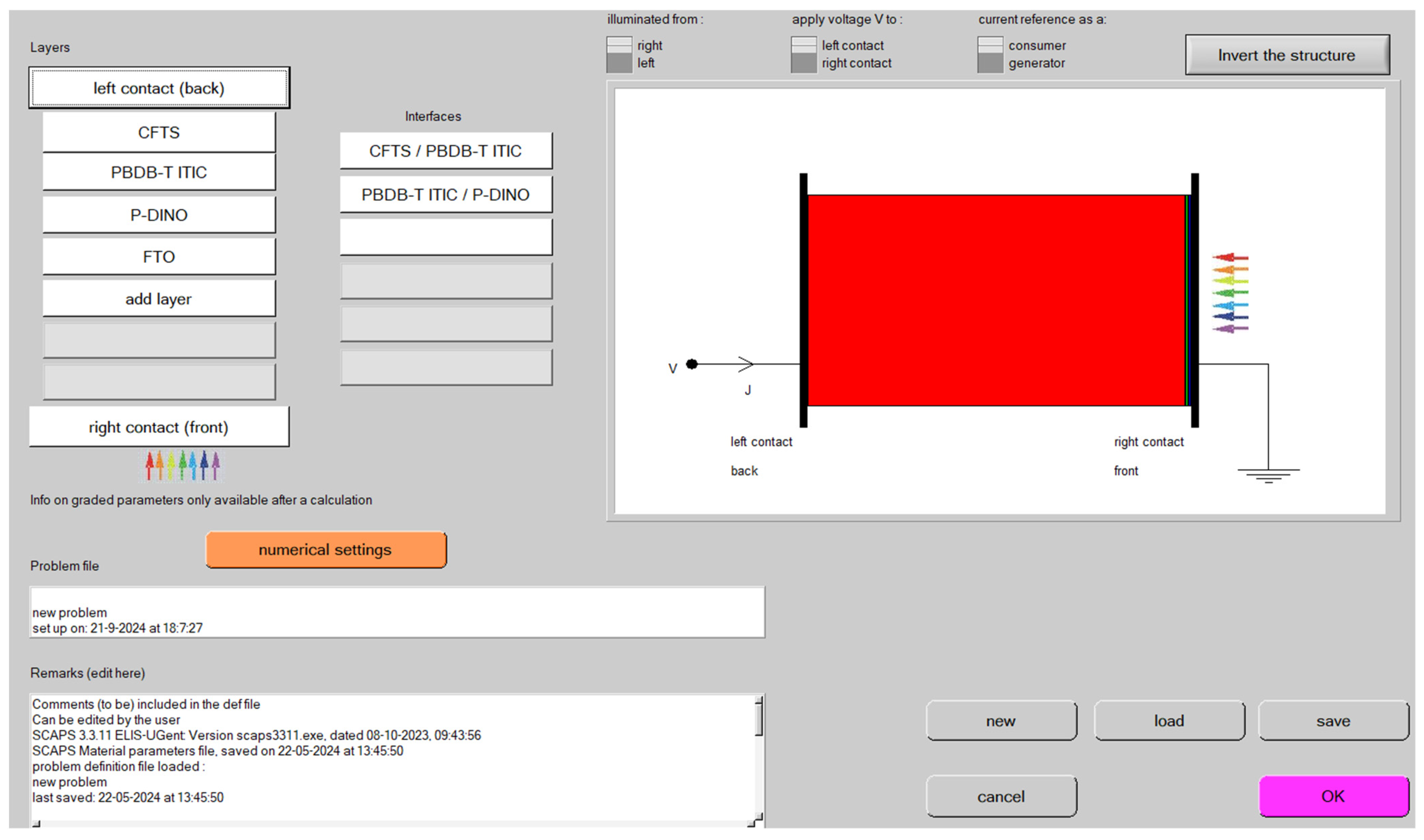
Herein, we present a numerical simulation using SCAPS-1D software (version 3.3.10) of a cell configured as follows: FTO/PDINO/PBDB-T/ITIC/CFTS/Al. The PDINO polymer was proposed as the ETL, while CFTS serves as the HTL, and PBDB-T/ITIC functions as an absorber. The PBDB-T/ITIC polymer blends were chosen as absorbers due to their excellent compatibility and exhibition of strong absorption in the visible spectrum. Furthermore, the materials enable effective charge separation and transport, which is essential for enhancing overall device performance. The influence of varying the defect density (Nt) of the absorber, the donor doping density (ND) of the electron transport layer (ETL), and the acceptor doping density (NA) of the hole transport layer was investigated. Moreover, the effect of changing the temperature, metallic back contacts, series, and shunt resistance on the performance of the device was also examined. Lastly, the capacitance voltage and Mott–Schottky’s characteristics of the modeled device were investigated. The results of this study are anticipated to greatly enhance the development of high-efficiency organic solar cells.
3. Results and Discussion
3.1. Thickness Optimization
In this work, we conducted a numerical simulation to explore the performance of a device with the following cell configuration: FTO/PDINO/PBDB-T/ITIC/CFTS/Al. Thickness optimization emerged as a significant component in improving solar cell performance, motivating the optimization of the thicknesses of the FTO, HTL, absorber, and ETL for the device [
34]. Thickness optimization involves systematically altering the thickness of various layers in the solar cell to achieve the optimization of parameters such as the PCE, FF,
JSC, and
VOC. Optimization was carried out repeatedly by altering the thickness of one layer at a time while maintaining a constant thickness of the other layers. The thickness optimization of the optimized device was carried out as follows: Initially, the thickness of CFTS was varied from 0.800 to 2.500 µm, while the thicknesses of FTO, PDINO, and PBDB-T/ITIC were held constant at 0.020, 0.500, and 0.300 µm, respectively. The optimal performance was achieved at a CFTS thickness of 2.400 µm, and then, it was fixed in the subsequent optimization of the other layers. The optimized thickness of CFTS was kept constant at 2.400 µm, while FTO and PBDB-T/ITIC were still maintained at the initial fixed values. Then, the thickness of PDINO was varied from 0.001 to 0.500 µm; the optimum thickness was obtained at 0.003 µm and fixed. After the optimization of the thickness of PDINO, the other layers’ thicknesses were maintained, and only PBDB-T/ITIC was altered from 0.008 to 0.300 µm, and the best thickness was achieved at 0.020 µm. Finally, the thicknesses of PDINO, PBDB-T/ITIC, and CFTS were maintained at their optimized values, while the thickness of the FTO layer was varied from 0.001 to 0.080 µm. The optimal performance was attained with an FTO thickness of 0.020 µm.
In general, a thicker absorber layer typically enhances light absorption, particularly for lower energy photons, which can contribute to a higher photocurrent. However, excessive thickness can lead to increased recombination losses, as the longer path for charge carriers to travel can result in more opportunities for carriers to recombine before reaching the electrode.
Similarly, the thickness of the HTL and ETL influences charge carrier transport. If these layers are too thick, they can increase the series resistance and impede efficient charge extraction, whereas overly thin layers may not provide sufficient support for charge separation. Optimal thicknesses are therefore necessary to balance these effects, ensuring effective charge transport while minimizing recombination. Additionally, the thickness of the layers can affect the overall device architecture and interface quality, which further impacts the performance. We have taken these factors into account when examining the trends observed in our simulations and have provided additional insights to better explain how each layer’s thickness influences the overall efficiency of the device. The results of the optimized and initial thicknesses of the devices are shown in
Table 3.
3.2. Current–Voltage (J-V) Characteristics
A J–V curve is a graphical representation that illustrates the relationship between the current density (
J) and the voltage (
V) of a photovoltaic device.
Figure 3a,b display the current–voltage (
J–V) characteristics of organic solar cells which were obtained from an initial and optimized simulation, respectively. The simulations were conducted based on the specific parameters detailed in
Table 1 and
Table 2. The J–V curves demonstrate how the performance of the devices changes with varying voltage, offering valuable insights into their efficiency and overall behavior during operation. The initial device demonstrated a PCE of 14.19%, which was considered relatively low, highlighting the necessity for optimization to improve its performance. After optimization, the device achieved a significant improvement in performance, with a PCE of 16.86%. This marked a noticeable enhancement compared to the initial PCE, demonstrating the effectiveness of the optimization process.
The high PCE of the optimized device was attributed to the optimized thickness of active layers, which ensured maximum light absorption while minimizing recombination losses. The optimized device not only showed an improved PCE but also achieved a fill factor of 79.12%, which is a key indicator of the device’s ability to convert the generated current into usable electrical power. A higher FF typically corresponds to lower losses and more efficient energy conversion. We can conclude that these findings emphasize the importance of fine-tuning device parameters to achieve better performance and provide valuable insights for the further optimization of organic solar cells.
3.3. Quantum Efficiency (QE) Curve
Quantum efficiency (QE) is a measure of how well a photovoltaic device transforms incident light into electrical energy [
39]. Specifically, it measures the quantity of charge carriers (electrons or holes) produced for each photon of light absorbed by the device. A greater percentage of incident photons are successfully converted into electrons when the QE is higher, increasing the cell’s total power generation [
40]. This is particularly important for improving solar cells’ energy conversion efficiency and making them more feasible for everyday use. The QE of the solar cell can be affected by various factors, including material properties, cell thickness, and fabrication quality. While the graphs primarily focus on the relationship between quantum efficiency and wavelength, resistance parameters, such as series resistance (
RS) and shunt resistance (
Rsh), can still influence the overall performance of the device, including the quantum efficiency. In general, series Rs can lead to a reduction in the quantum efficiency at higher current densities because it causes losses in the form of heat and decreases the voltage output. Rsh, on the other hand, typically impacts the device’s leakage current, which can decrease the overall efficiency of the solar cell.
Figure 4a,b demonstrate the quantum efficiency curves for the initial and optimized simulation of the proposed solar cell, respectively.
Figure 4a, the QE of the initial device, reveals a significant increase in the QE of the device from 75.90 to 90.48% between 300 and 850 nm, followed by a decline from 860 to 900 nm. The decline from 860 to 900 nm might be due to the device exhibiting strong absorption in the 300 to 850 nm range, which allows for efficient charge carrier generation, thus resulting in a higher QE. However, as the wavelength increases beyond 850 nm, the material may become less effective at absorbing light of an extended wavelength, leading to a decline in the QE. This decrease in the QE above 850 nm emphasizes how important it is to use technical techniques to increase the absorption range of solar cells. These techniques could include the adoption of multijunction cell designs to enhance performance and increase applicability in a variety of environmental conditions.
On the other hand,
Figure 4b shows that the optimized device had a high QE of above 90% between 300 and 800 nm, implying that the device can absorb both infrared and visible light radiation. It can also be observed that the QE increased from 96.46 to 97.72% in the wavelength range of 300 to 360 nm, after which it decreased up to 900 nm. The initial increase in the QE may be attributed to enhanced photon absorption and improved charge carrier mobility within the device at these shorter wavelengths. The subsequent decline could result from increased recombination rates or decreased material reactivity at longer wavelengths. It also shows that the cell cannot adequately absorb light at these wavelengths.
When comparing the quantum efficiency across different organic materials, it is evident that devices utilizing high-performance organic semiconductors, such as perovskite or non-fullerene acceptors, can achieve improved QE values, approaching those of conventional inorganic solar cells. Perovskite solar cells (PSCs) have garnered significant attention due to their excellent optical and electronic properties, which result in high quantum efficiency. Compared to traditional silicon solar cells, PSCs exhibit a broader absorption spectrum and superior light absorption at a lower material cost. The quantum efficiency in PSCs can reach over 90% under optimal conditions, particularly in the visible range. However, perovskite materials are still under investigation in terms of long-term stability and resistance to environmental degradation, which can affect their long-term quantum efficiency and overall performance. On the other hand, silicon-based solar cells have been the dominant technology for decades, with high stability and efficiency. The quantum efficiency of silicon solar cells can range from 80% to 90% under standard test conditions, especially in the infrared and visible ranges. However, silicon cells have an inherent limitation due to their indirect band gap, leading to less efficient light absorption, particularly for wavelengths longer than 1100 nm.
3.4. Impact of the Defect Density of an Absorber on Performance
Defects can have a substantial impact on the device’s electrical characteristics and overall performance, particularly the charge carrier mobility and recombination rates [
41]. Understanding the effect of defect density within the absorber layer is crucial in enhancing solar cell efficiency and stability. To determine the optimal defect density for the simulated cell, the absorber defect density was varied from 1 × 10
9 to 1 × 10
15 cm
−3, and the characteristic results are graphically presented in
Figure 5. In
Figure 5a, it can be noted that the PCE remained constant at 16.87% from the 9th to 12th order of density of defects levels. However, from the 13th to 14th order, the PCE slightly decreased from 16.79 to 16.28%. This was followed by a more significant decrease to 14.94% for the 15th order. The observed dip in the PCE as a function of the increasing density of defects may be attributed to the fact that as the defect density order increases, an accumulation of defects within the absorber material may result in reduced charge carrier mobility and increased recombination losses, therefore affecting the overall performance of the cell. It was also observed that the FF (
Figure 5b) values of the modeled cell decreased with the increase in the defect density of the absorber. The decrease in the FF may be assigned to a high defect density, which negatively impacts charge carrier dynamics and increases the recombination of electrons and holes. Furthermore, defects within the cell trap charge carriers, thereby reducing the number of carriers available to contribute to the current. The optimal defect density of the modeled cell was at 10
9 cm
−3, where the maximum FF of 79.15% was obtained.
Figure 5c demonstrates that as the defect density within the device rises, the
JSC remains constant between the 9th and 12th orders before declining between the 13th and 15th orders. The decline occurred because of the trap, which tends to seize charge carriers, preventing them from participating in the solar cell’s current flow. The maximum permissible defect density for the device was observed between the 9th and 12th orders, where the highest short-circuit current density (
JSC) reached 33.19 mAcm
−2. It was also observed that the
VOC (
Figure 5d) decreased as the defect density of the absorber increased. This may be due to higher series resistance within the device, affecting the
VOC by impeding the current flow. Furthermore, a higher defect density often results in higher recombination rates for charge carriers. This recombination process diminishes the quantity of charge carriers available for collection by the solar cell, therefore reducing both the
VOC and
JSC. A higher defect density facilitates the recombination of electrons and holes, which hinders the ability to generate current efficiently and lowers the
VOC.
The observed decrease in the VOC with increasing defect density can be attributed to two main factors. First, an increase in the defect density typically leads to higher series resistance within the device, which impedes the current flow and results in a reduction in the VOC. Second, higher defect densities increase charge carrier recombination rates, reducing the number of available charge carriers for collection by the solar cell. This recombination process also contributes to the observed decrease in both the VOC and JSC. As the defect density increases, defects within the absorber layer create trap states that impede charge carrier mobility, increasing recombination rates and effectively reducing the number of carriers contributing to the current. This results in the observed decline in performance parameters such as the PCE, FF, and JSC at higher defect densities. Moreover, the increased defect density leads to higher series resistance, which in turn affects the open-circuit voltage (VOC).
3.5. Effect of ETL Donor Density Doping Levels
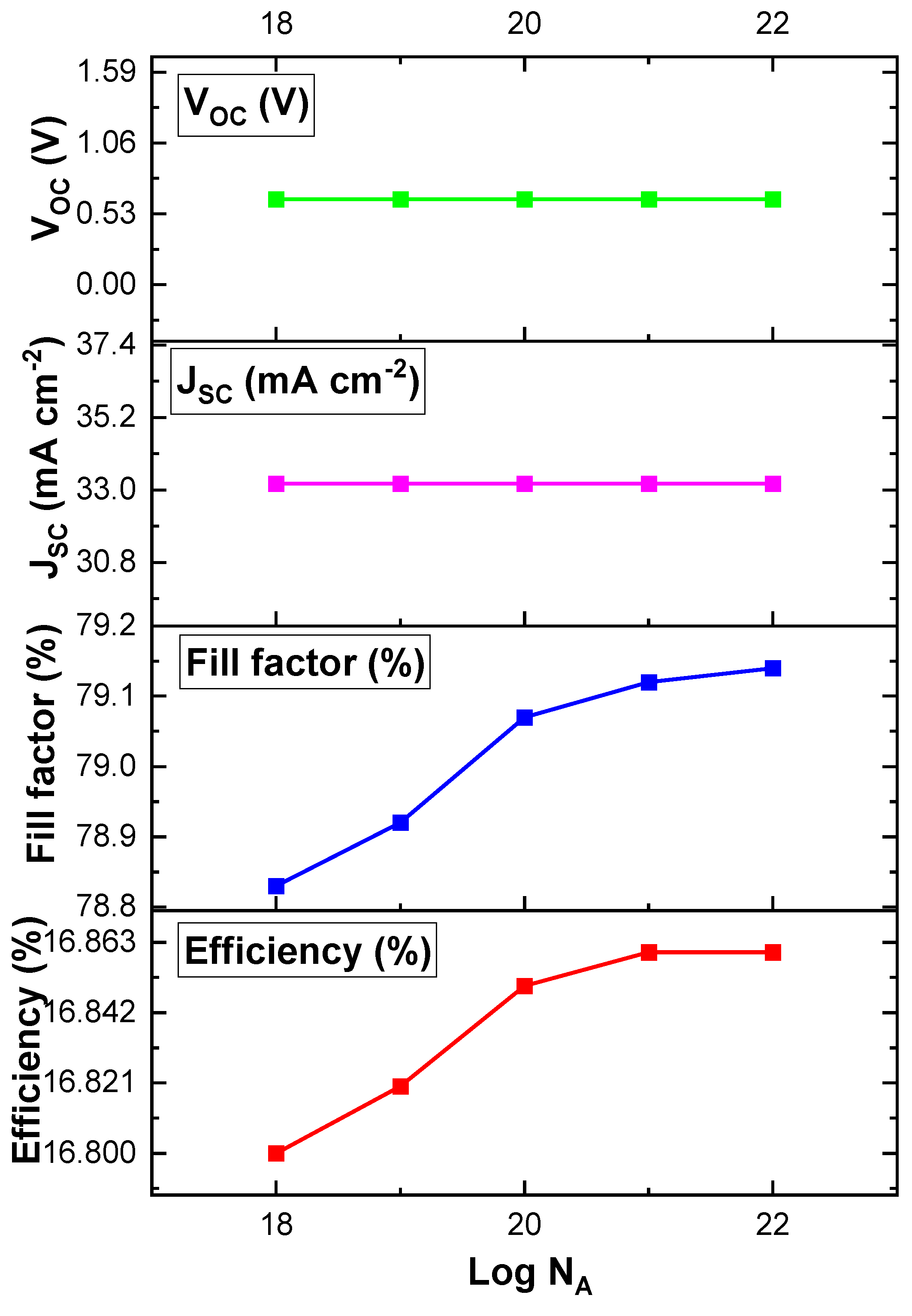
Varying the donor density doping levels in an ETL can significantly impact the performance of the device. The effect of doping the ETL was also examined by varying the donor density doping levels from the 18th to the 24th order, while the acceptor density was kept constant at 1 × 10
19 cm
−3; the results are presented in
Figure 6.
Figure 6 shows an increase in the PCE and FF values as the donor density increases from the 18th to the 22nd order which was ascribed to the fact that an optimal donor density ensures the efficient excitation of electrons from the valence band to the conduction band, increasing the overall photogenerated current. Ideally, suitable donor density doping levels can improve charge carrier availability while reducing recombination losses. The optimal donor density was 10
22 cm
−3, which yielded a PCE of 16.86%, corresponding to an FF of 79.14%.
Figure 6 revealed that the
VOC and
JSC remained constant at 0.64 V and 33.19 mA cm
−2, respectively, across all orders, an indication that when the donor density reaches an optimal level, a further increase may not significantly affect the internal potential, hence, keeping the
VOC and
JSC constant. It can be also noted that for the 23rd and 24th orders, the device did not show any photovoltaic parameters, which might be due to the detrimental recombination of photogenerated charges, leading to the insufficient generation of charge carriers.
3.6. Effect of Acceptor Density Doping Level of HTL
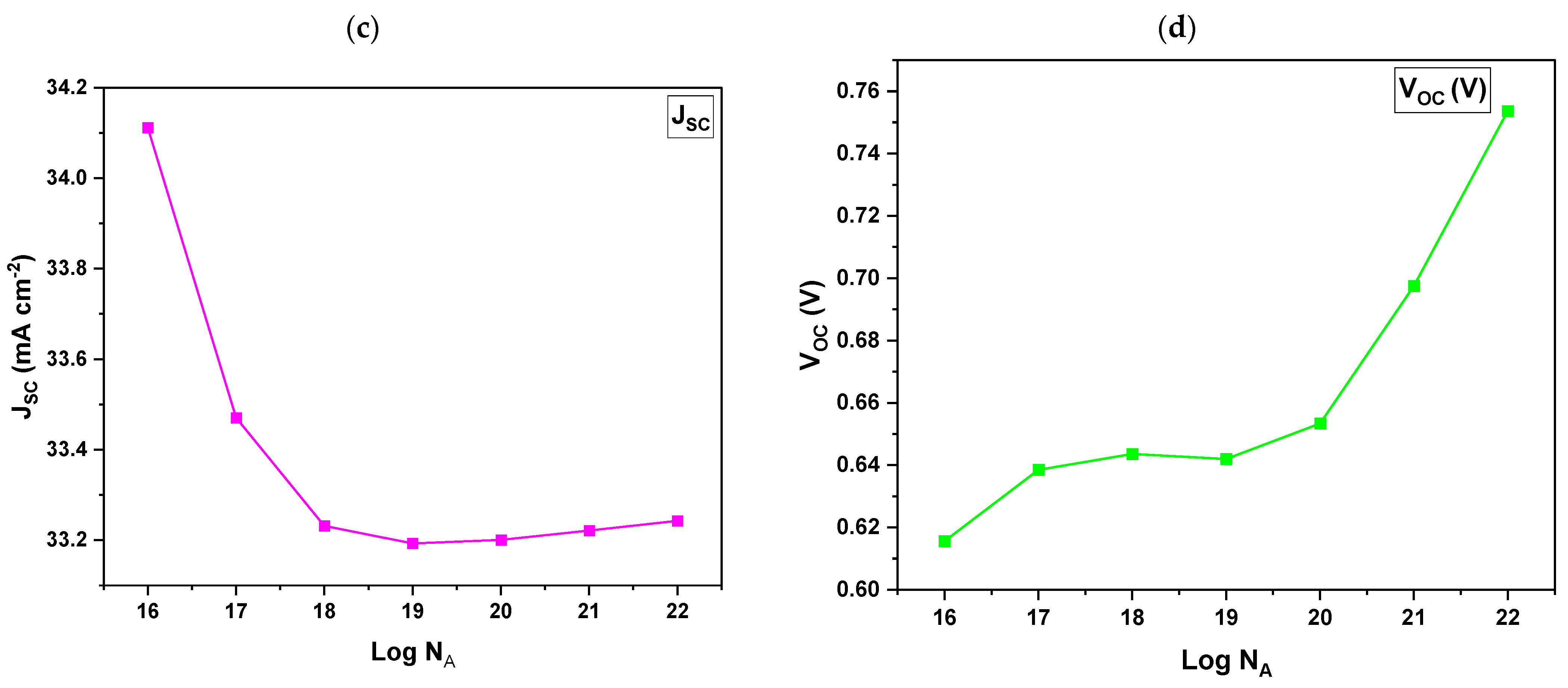
The acceptor density doping level is a significant factor affecting charge transport and recombination within the cell. In the optimization of the acceptor density, the donor density was maintained at 1 × 10
21 cm
−3. This approach allows for a focused examination of how varying the acceptor density impacts the overall performance of the solar cell. By keeping the donor density fixed, we can distinguish the effects of acceptor doping on important parameters such as the charge carrier concentration, recombination rates, and the electric field distribution within the solar cell device. A higher acceptor density may improve the separation of photogenerated charge carriers, thus lowering the possibility of recombination, resulting in a higher PCE.
Figure 7a shows that as the PCE increases, the acceptor density increases, with the 22nd order attaining the highest PCE value of 21.24%. The increase in the PCE could be due to improved charge carrier dynamics. As the acceptor density increases, the device may experience better charge collection and reduced recombination losses. This leads to higher efficiency in converting light into electricity. It was also noted that the FF (
Figure 7b) increased with an increase in the acceptor density. The reason behind the increase in the FF might be the enhanced mobility of charge carriers when the acceptor density is optimized, enabling their transport to the appropriate electrodes, therefore increasing the FF.
Figure 7c illustrates a trend in the
JSC values. Initially, there is a noticeable decrease in the
JSC from the 16th to the 18th order, indicating a potential decline in charge carrier generation during this range. The
JSC experiences another reduction at the 19th order. However, from the 20th to the 22nd order, the
JSC values begin to increase again. This pattern suggests that while certain orders may lead to inefficiencies, subsequent adjustments or optimizations in the material can enhance charge carrier dynamics, ultimately improving the overall current density. It was also observed that the
VOC (
Figure 7d) increased with an increase in the acceptor density. The increase in the
VOC can be explained by higher acceptor density, which enhances hole mobility, resulting in more efficient charge transport and a reduction in recombination losses.
3.7. Impact of Varying Working Temperature
The ambient temperature has a considerable impact on the performance of a photovoltaic device, influencing various aspects of its operation and performance [
36]. The numerical simulation of the solar cell devices examined in this work was performed at a temperature of 300 K. However, to further understand the performance characteristics, simulations were also carried out from 240 to 400 K to investigate the impact on the cell’s output characteristics. This method enables us to evaluate how different thermal conditions affect the efficiency and operation of solar cells, providing crucial insights into their operational stability and performance across a wide range of ambient temperatures. At the initial temperature of 240 K, the device did not exhibit any photovoltaic behavior. Hence, to explore the impact of temperature on the absorber’s performance, the temperature was subsequently varied from 260 to 400 K. The main reason for simulating these cells over this temperature range was to ensure their reliable performance in diverse environmental conditions.
Figure 8 shows the results of the photovoltaic parameters at different operating temperatures.
In general, the efficiency of solar cells decreases with an increase in temperature because of enhanced electron–photon interactions, decreased open-circuit voltage, and higher leakage currents.
Figure 8a illustrates the graphical representation of the PCE versus temperature. From the graphs, it can be noted that as the temperature increases, the PCE of the device decreases. The temperature decreased from 17.31 to 15.64%. The decline in the PCE may be attributed to increased recombination rates of charge carriers at higher temperatures, resulting in a reduction in the overall performance of the cell. Thermal expansion might also trigger structural changes in the cell that affect charge transport pathways, therefore limiting effective electron flow. On the other hand, the FF (
Figure 8b) decreased from 80.97 to 74.77%. The observed decrease in the FF may be due to higher temperatures that may cause larger resistance losses within the device due to increased series resistance, reducing the FF.
According to Chander et al. [
42], the
JSC is directly proportional to the number of photogenerated charge carriers, which also tends to increase with the operating temperature in solar cells.
Figure 8c demonstrates how temperature variations influence the
JSC. The results reveal that the
JSC increased with an increase in temperature. The observed behavior of an increase in the
JSC may be ascribed to the rise in temperature, which increased the thermal energy available to the semiconductor material, facilitating the excitation of electrons from the valence band to the conduction band. This thermal promotion enhances the generation of both electrons and holes, resulting in a higher
JSC.
Figure 8d shows a decrease as the temperature increased. The decrease in the
VOC may be due to higher carrier densities that may lead to increased electron–hole recombination loss, therefore decreasing the
VOC. Overall, regardless of the increased
JSC, as the temperature increased, other photovoltaic parameters such as the PCE, FF, and
VOC decreased. Therefore, precise thermal control is essential to ensuring the long-term stability and optimal performance of OSC devices, particularly in real-world operating conditions.
3.8. Impact of Varying Series and Shunt Resistance
Figure 9 illustrates the impact of the series and shunt resistance on the proposed solar cell. The series resistance (
Rs) was changed from 0 to 5 Ω cm
2, while the shunt resistance (
Rsh) was kept constant at 10
6 Ω cm
2. At the same time, in order to also examine the effect of shunt resistance on performance, the series resistance was kept constant at 0.5 Ω cm
2, while the shunt resistance values were varied from 10
1 to 10
6 cm
2 [
43].
Figure 9a shows the effect of shunt resistance, varied from 10
1 to 10
6 Ω cm
2. As the R
sh increased from 10
1 to 10
6 Ω cm
2, all photovoltaic parameters significantly increased, until they plateaued at about 3 Ω cm
2 up to 6 Ω cm
2 values. The PCE increased from 2.63 to 16.37% from 10
1 to 10
4 Ω cm
2 before becoming constant at 16.40% at 10
5 and 10
6 Ω cm
2. The rise in the PCE from 2.63 to 16.37% indicates improved charge carrier generation and collection, probably due to the device structure’s optimization. The FF had a rapid increase from 25 to 65.51%, followed by a gradual increase from 75.68 to 76.81%, with values ranging from 10
3 to 10
6 Ω cm
2. The significant increase in the FF from 25 to 65.51% indicates an important enhancement in the output balance between the current and voltage, which may be caused by enhanced charge transport capabilities and reduced shunt resistance. The
JSC increased from 31.67 to 33.23 mA cm
2 at 10
1 to 10
3 Ω cm
2, stabilizing at a value of 33,25 mA cm
−2 from 10
4 to 10
6 Ω cm
2. The
VOC increased from 0.33 to 0.63 V from 10
1 to 10
2 Ω cm
2 until reaching a constant value at 0.64 V for the remaining tested shunt resistance.
Figure 9b shows the effect of series resistance, varied from 0 to 5 Ω cm
2. It can be observed that as the
Rs increases, the PCE significantly decreases from 16.89 to 12.17%, and the FF decreases from 79.12 to 57.02% at a series resistance of 0 to 5 cm
2. A high R
s may indicate reduced effective charge collection, leading to increased current leakage. However, the
JSC and
VOC remained constant at 33.25 mA cm
−2 and 0.64 V, respectively. The reason for the constant values of the
JSC and
VOC may be due to the absence of significant increases in recombination losses that can help maintain both the
JSC and
VOC at constant levels.
3.9. Impedance Analysis
In perovskite solar cells, the layers that extract charges play a crucial role in the overall performance of the device. The HTL is particularly important, as it facilitates the movement of positively charged holes generated in the perovskite layer toward the electrode. This process significantly influences both the efficiency and stability of the solar cell [
44]. Impedance analysis provides an essential understanding of several aspects of the solar cell, including interfacial resistance, recombination losses, charge trapping and transport, and degradation mechanisms [
45]. Impedance measurements assist in identifying resistive losses at interfaces between different layers. Elevated interfacial resistance impedes effective charge transport, reducing the overall performance of the solar cell.
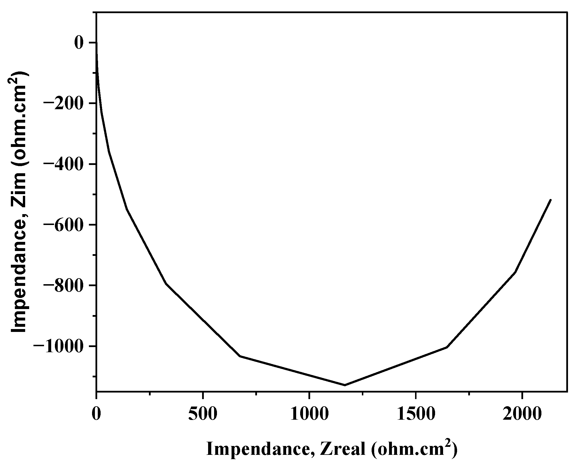
The impedance spectrum (Nyquist plot) of the model cell device was analyzed displaying the complex plane plot (Z imaginary versus Z real), as demonstrated in
Figure 10. The curve has a pronounced U shape, as commonly observed in Nyquist plots, which is associated with the charge transfer mechanism within the solar cell, which depicts the interactions between electrons and ions at the interface of the electrolyte and the electrode. In the lower frequency range, diffusion processes dominate the resistance, resulting in the ascending arm of the U, whereas at higher frequencies, the descending arm of the U represents charge transfer resistance. The U-shaped impedance profile offers unique insights into the kinetic processes that occur within the solar cell device. The analysis of the Nyquist plot revealed that as the Z real value increased from 0 to 1166.69 ohm.cm
2, the Z imaginary decreased, after which it increased again. The decrease in the Z imaginary suggests enhanced charge transport and lower resistive losses within the cell. The subsequent increase in the Z imaginary at higher Z real values may possibly be due to charge accumulation effects or slower dynamic processes within the device. This behavior underscores the complex interactions between charge transport, recombination, and other factors affecting the overall performance of the solar cell.
3.10. Effect of Using Various Metal Back Contacts
The choice of aluminum (Al) as a back metal, which has a work function of 4.26 eV, was driven by its properties. Firstly, it has excellent thermal conductivity, which helps in maintaining performance under varying temperatures. Secondly, aluminum has good electrical conductivity, which helps in efficiently collecting and transporting the generated current. Thirdly, Al can be susceptible to corrosion. Furthermore, Al is relatively inexpensive and widely available compared to many other metals. In addition to the beneficial characteristics of Al, various alternative metals could be explored for specific applications or to improve certain aspects of solar cell performance. For instance, metals like silicon and cobalt are known for their excellent conductivity and could enhance the current collection efficiency.
Several factors, including economic considerations, performance needs, and ease of integration into current manufacturing processes, determine the choice of back metal.
Table 4 presents the performance data of different metal back contacts, including tin (Sn), silicon (Si), ruthenium (Ru), manganese (Mn), and cobalt (Co), when incorporated into the proposed solar cell architecture. It can be noted that Si and Co perform better than any other metal back contact in terms of producing a higher PCE of 18.12% with all other photovoltaic parameters being the same. Ru gave a modest PCE of 17.81%. The lowest performing metals were Sn and Mn, exhibiting a PCE of 16.86 and 16.60%, respectively. The different PCEs observed when changing the back metal contact can be attributed to several factors related to the material properties of the metal contacts and their interaction with the semiconductor layer in the solar cell. It can be observed from
Table 4 that the higher the work functions, the higher the percentage of the device. It was also noted that Si and Co exhibited the same PCE (18.12%), which may be attributed to their close work function values. Generally, the
VOC remained constant for all the devices. The fact that the open-circuit voltage (
VOC) remained constant across different back metal contacts might be due to the fact that certain factors, such as the semiconductor’s intrinsic properties or the built-in potential at the junction, are not significantly influenced by the change in the metal contact.
3.11. Comparative Studies
The present study includes a comparison with the performance of PBDB-T: ITIC-based solar cells from the literature, as reported in
Table 5. The results show different cell configurations for both experimental and simulation data. The data indicate that the solar cell model proposed in this study achieves moderately high electrical parameters when compared to other devices shown in
Table 5, with a PCE of 16.86%. As can be seen from
Table 5, the performance of PFN-based solar cells is still low. Therefore, additional theoretical and experimental strategies are necessary to improve their performance. The low performance of the experimentally fabricated PFN-based devices may be attributed to poor stability resulting from exposure to harsh weather conditions, including moisture, light, and heat.
4. Conclusions
In this study, an organic solar cell with a general structure of FTO/PDINO/PBDB-T/ITIC/CFTS/Al was simulated using SCAPS-1D software. Various aspects such as the thickness of PBDB-T/ITIC (active layer), PDINO (ETL), CFTS (HTL), and FTO (conductive substrate), the donor density of the ETL and acceptor density of the HTL, the temperature, the metal back contacts, and the series and shunt resistance were systematically varied, and the device performance was optimized. The J–V characteristics of organic solar cells were simulated both initially and after optimization, based on the parameters outlined in
Table 1 and
Table 2. The optimization improved the PCE from 14.19% to 16.86%, with a fill factor of 79.12%, due to optimized active layer thickness and reduced recombination losses. The QE of the organic solar cell was analyzed through initial and optimized simulations. The optimized device achieved a higher QE of above 90% in the 300–800 nm range, with an increase from 96.46% to 97.72% between 300 and 360 nm, while the initial device showed a QE of 75.90% to 90.48% between 300 and 850 nm, with a decline after 850 nm. These results highlight the significance of parameter optimization in enhancing the performance of organic solar cells and improving light absorption across a broader spectrum. This study demonstrated that increasing the defect density in the absorber layer negatively affects the performance of the organic solar cell, leading to a decrease in the PCE, FF,
JSC, and
VOC. The optimal performance was observed at a defect density of 1 × 10
9 cm
−3, where the cell achieved maximum values for these parameters. Higher defect densities increased the recombination rates and series resistance, limiting charge carrier mobility and reducing overall efficiency.
Varying the donor density doping levels in the ETL improved the device performance, with the optimal donor density of 1022 cm−3 resulting in a PCE of 16.86% and an FF of 79.14%. Beyond this optimal density, the VOC and short-circuit current density, JSC, remained constant. At higher doping levels, 23rd and 24th orders, the device showed no photovoltaic performance, likely due to the excessive recombination of photogenerated charges. Varying the acceptor density doping level in the solar cell significantly impacted the performance, with the highest PCE of 21.24% achieved at the 22nd order. This improvement was attributed to better charge carrier dynamics, enhanced charge collection, and reduced recombination losses. The FF also increased with optimized acceptor density, suggesting improved charge transport. Additionally, both the JSC and VOC showed an overall increase, with the VOC benefiting from enhanced hole mobility and reduced recombination. The impact of ambient temperature on the performance of photovoltaic devices was examined by simulating solar cell behavior over a temperature range of 240 to 400 K. Increasing the ambient temperature from 240 to 400 K led to a decrease in the PCE and FF due to higher recombination rates and increased resistance losses. While the JSC increased with temperature, the VOC decreased due to increased carrier recombination.
The effects of series and shunt resistance on the performance of the proposed solar cell were also examined. When the Rsh was increased from 101 to 106 Ω cm2, the PCE improved significantly, reaching 16.37%, with the FF rising from 25% to 76.81%. The JSC and VOC also showed improvements but stabilized at higher resistance values. Conversely, as the Rs was increased from 0 to 5 Ω cm2, the PCE and FF decreased, with the Rs leading to reduced charge collection, though the JSC and VOC remained stable. The Nyquist plot reveals a U-shaped curve, representing charge transfer resistance at higher frequencies and diffusion resistance at lower frequencies. As the Z real value increased, the Z imaginary initially decreased, indicating improved charge transport, before rising again at higher Z real values, potentially due to charge accumulation or slower dynamics. This analysis provides valuable insights into the factors influencing solar cell performance, including charge transport and recombination. To evaluate the impact of different back metal contacts on solar cell performance, several metals were tested, including Al, Si, Co, Ru, Mn, and Sn. Each metal was assessed for its ability to enhance the device’s efficiency, with specific attention to the parameters. The results revealed that Si and Co exhibited the highest performance, both achieving a PCE of 18.12%, which was superior to the other metals tested. Interestingly, the VOC remained constant across all the back metal contacts, indicating that factors like the semiconductor’s intrinsic properties or the built-in potential at the junction had a more significant effect on the VOC than the choice of back metal. The overall findings highlight the importance of selecting materials with suitable work functions to optimize solar cell efficiency while also considering factors like cost and ease of integration.


 ,
, 


