1. Introduction
HfO
2 is an important material in the field of optical thin films and has received increasing attention in recent years due to its large band gap (~5.8 eV) [
1], extensive transparent spectral range from the ultraviolet to infrared regions, and good chemical stability [
2]. Therefore, it has excellent application prospects in industrial laser processing, gravitational wave detection [
3,
4], inertial confinement fusion [
5,
6], laser gyroscopes [
7], and various other domains, where HfO
2 serves as the high-refractive-index component in multilayer optical coatings including mirrors, anti-reflection systems, and beam splitters. In many of these applications, the films are exposed to ambient air rather than being encapsulated in inert environments, making air-atmosphere stability critical for practical performance.
Considerable work has been conducted to investigate the properties of HfO
2 films prepared by different deposition techniques [
8,
9,
10,
11,
12,
13]. Researchers have found that in the field of pulsed laser applications, HfO
2 thin films deposited via evaporation exhibit a higher laser damage threshold compared to those produced by sputtering [
14]. When HfO
2 thin films are deposited through evaporation, metallic Hf is utilized as the evaporation source, while oxygen is introduced into the vacuum chamber for reactive deposition during the process, leading to a reduction in nodal defects. This results in an improved laser damage threshold [
15]. At the 1064 nm wavelength, damage to thin films from nanosecond pulsed lasers may arise from light absorption and nodal defects [
16,
17]. The inherent absorption of 1064 nm light by HfO
2 thin films presents a significant obstacle in enhancing the damage threshold of the films [
18,
19].
Defects such as discontinuous microstructural growth morphology [
20,
21], inhomogeneous refractive index profiles [
22,
23], atomic vacancies [
1,
24], and impurities [
25] can adversely affect the optical properties of the films [
26,
27]. Specifically, oxygen vacancies (V
O) are believed to contribute to increased absorption in the films [
28,
29]. While the presence of V
O in HfO
2 has been widely reported, the relationship between deposition conditions, structural phases, and vacancy concentration has not been systematically established.
In this study, the electron density of states and extinction coefficient of amorphous HfO2 films, both with and without VO, were investigated using first-principles calculations. The HfO2 films were prepared using electron beam evaporation and plasma-assisted deposition methods. The impact of various deposition techniques and preparation parameters on the phase and optical properties of the films was analyzed through experimental characterization of the samples. Additionally, a systematic demonstration through combined theoretical and experimental approaches was conducted, showing that the crystallization of amorphous HfO2 enhances VO and optical absorption. A preparation method for low-absorption HfO2 thin films with the potential for excellent stability in practical applications was also proposed.
2. Materials and Methods
The electron density of states and extinction coefficient of the HfO2 structure were calculated using density functional theory as implemented in the Vienna Ab initio Simulation Package. The Perdew–Burke–Ernzerhof functional within the generalized gradient approximation was employed for exchange–correlation interactions. Amorphous HfO2 structures were generated through molecular dynamics simulations using a systematic melt-quench protocol. Starting from a 2 × 2 × 2 supercell of monoclinic HfO2 containing 96 atoms, the system was heated to 3500 K with a canonical ensemble (NVT) to achieve complete structural disorder, followed by rapid quenching to 300 K to prevent crystallization. VO effects were modeled by removing single oxygen atoms from the relaxed amorphous structure, yielding vacancy concentrations of approximately 1.56%. Final structures, both with and without VO, underwent relaxation to optimize local bonding while preserving the amorphous network topology. Given that each oxygen atom within the amorphous structure of HfO2 thin films may exist in distinct local environments, calculations were performed solely for the scenario in which a single oxygen atom was removed, thereby providing an approximate evaluation of the influence of VO on the optical properties of the films.
HfO
2 thin films were fabricated utilizing both E-beam evaporation (EBE) and plasma-assisted deposition (PAD) technology. The deposition processes were conducted using the Leybold Optics Syruspro1510 coating machine, which is equipped with two electron guns, a source that generates plasma by introducing argon gas, and ceramic heaters. High-purity oxygen (>99.999%) was introduced into the chamber during the coating process. High-purity hafnium metal (>99.95%) served as the source material, while fused quartz was used as the substrate. The initial background vacuum of the coating process was 1 × 10
−6 mbar. The deposition rates were precisely controlled at 0.2 nm/s using quartz crystal microbalance sensors, with target film thicknesses set at 300 nm. Five distinct samples were prepared with varying deposition parameters, primarily involving adjustments in substrate temperature (120, 160, 200 °C), oxygen flow rate (5, 10 sccm), and the presence of plasma assistance, as detailed in
Table 1. The deposition parameters were systematically varied to investigate the effects of key processing variables on film structure and optical properties. Among these samples, HfO
2-D (160 °C substrate temperature, 10 sccm oxygen flow, with plasma assistance) served as the baseline sample, with the remaining samples varying individual parameters to isolate their effects on film properties. Compared to the baseline sample, HfO
2-A was deposited without plasma assistance (using the EBE method). HfO
2-B was prepared with a reduced oxygen flow rate of 5 sccm. HfO
2-C was deposited at a lower substrate temperature of 120 °C, whereas HfO
2-E was deposited at an elevated temperature of 200 °C. This systematic variation allows us to decouple the effects of oxygen stoichiometry, plasma bombardment, and deposition temperature on film crystallinity and absorption.
The transmittance of the HfO
2 thin film samples was measured using a Lambda 950 spectrophotometer from PerkinElmer. The optical constant as a function of wavelength was derived from the transmittance curves using the Forouhi–Bloomer (F-B) dispersion model [
30], which is specifically designed for amorphous and dielectric materials in addition to the Swanepoel model [
31].
The absorption of the films at 1064 nm was assessed using a laser calorimetric technique with a continuous wave Nd:YAG laser at 1064 nm. The absorption was determined by measuring the temperature rise of the sample under laser illustration using a high-sensitivity thermocouple. The absorption is reported in parts per million (ppm).
X-Ray diffraction (XRD) patterns of the samples were obtained using a Bruker D8 Advance X-Ray diffractometer with Cu Kα radiation (λ = 1.5406 Å) operating at 40 kV and 40 mA. Grazing incidence X-Ray diffraction (GIXRD) geometry was employed with a fixed incident angle of 1° to enhance surface sensitivity and minimize substrate contributions. The 2θ scanning range was 10–70° with a step size of 0.02° and a counting time of 1 s per step. Emission spectra were captured with an iHR320 spectrograph (Jobin Yvon, Inc.) equipped with a 193 nm excitation light source.
X-Ray photoelectron spectroscopy (XPS) measurements were performed using a Thermo Scientific K-Alpha XPS system with Al Kα radiation (1486.6 eV). High-resolution spectra of the Hf 4f and O 1s regions were acquired to determine the chemical states of hafnium and oxygen. The XPS depth of approximately 10 nm represents only the near-surface region of the films.
The cross-sectional structures of the samples were examined using a SIGMA HD scanning electron microscope (SEM) from Zeiss. Cross-sectional slices were prepared using a Thermo Scientific Helios 5 CX focused ion beam (FIB), and transmission electron microscopy (TEM) images were obtained with the Talos F200S G2 device. Selected area electron diffraction (SAED) patterns were obtained during TEM analysis to definitively distinguish between amorphous and crystalline structures.
The annealing processes for the samples were conducted in a tube furnace, with a temperature ramp rate of 5 °C/min until reaching 400 °C, followed by a 6 h hold at this temperature and natural cooling to room temperature. The furnace was calibrated by K type thermocouples prior to experiments, and the temperature uniformity in the sample region was verified to be within ±3 °C. All annealing processes were performed under ambient atmospheric conditions.
3. Results and Discussion
During the preparation of HfO
2 thin films using either the EBE or PAD methods, it is common for the films to exhibit an amorphous structure [
1,
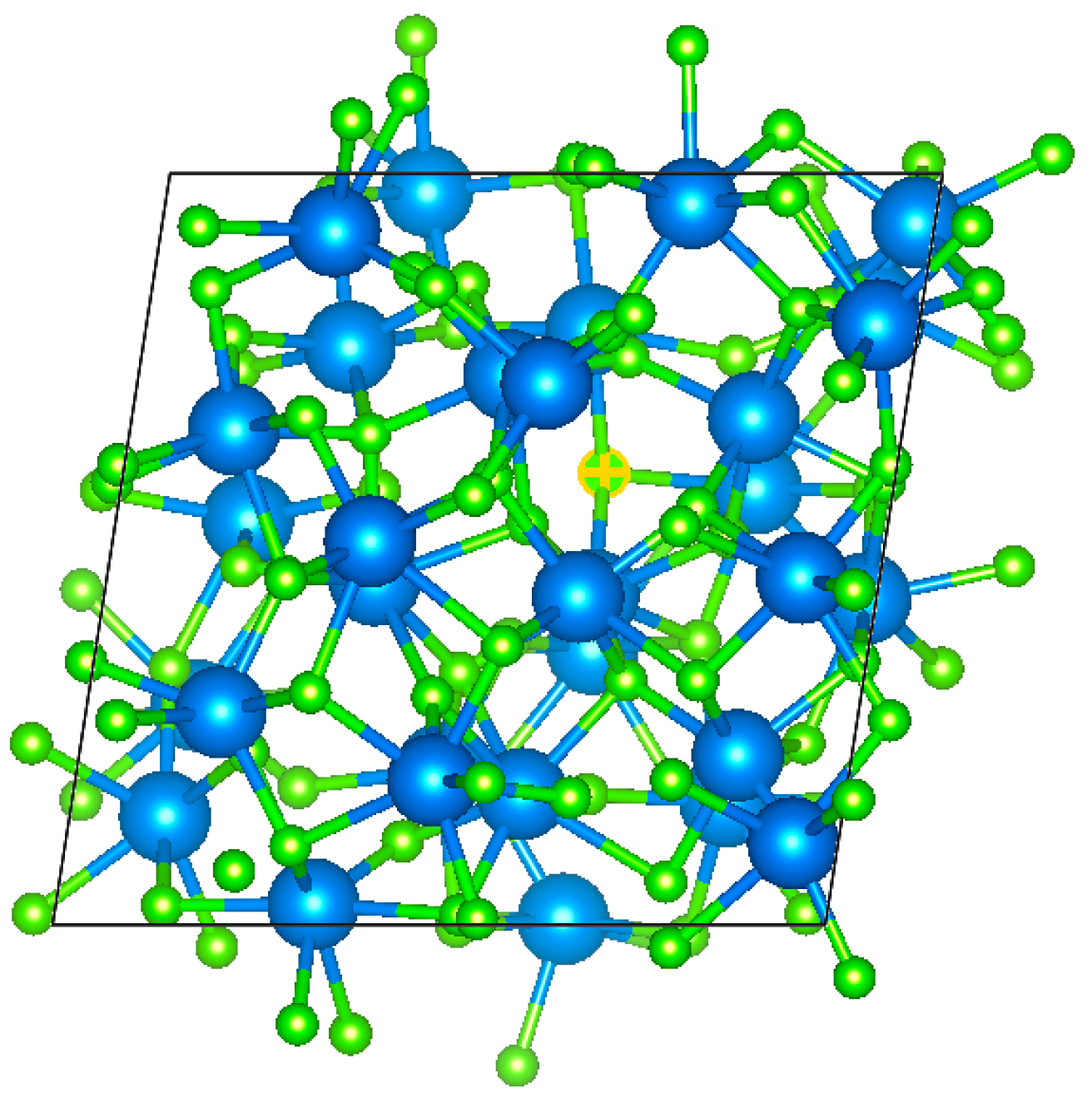
20]. Molecular dynamics simulations were conducted to generate an amorphous structure model of the HfO
2 thin film. To simulate the optical effects of V
O in the HfO
2 film, one oxygen atom was intentionally removed, resulting in a V
O concentration of 1/64, as illustrated in
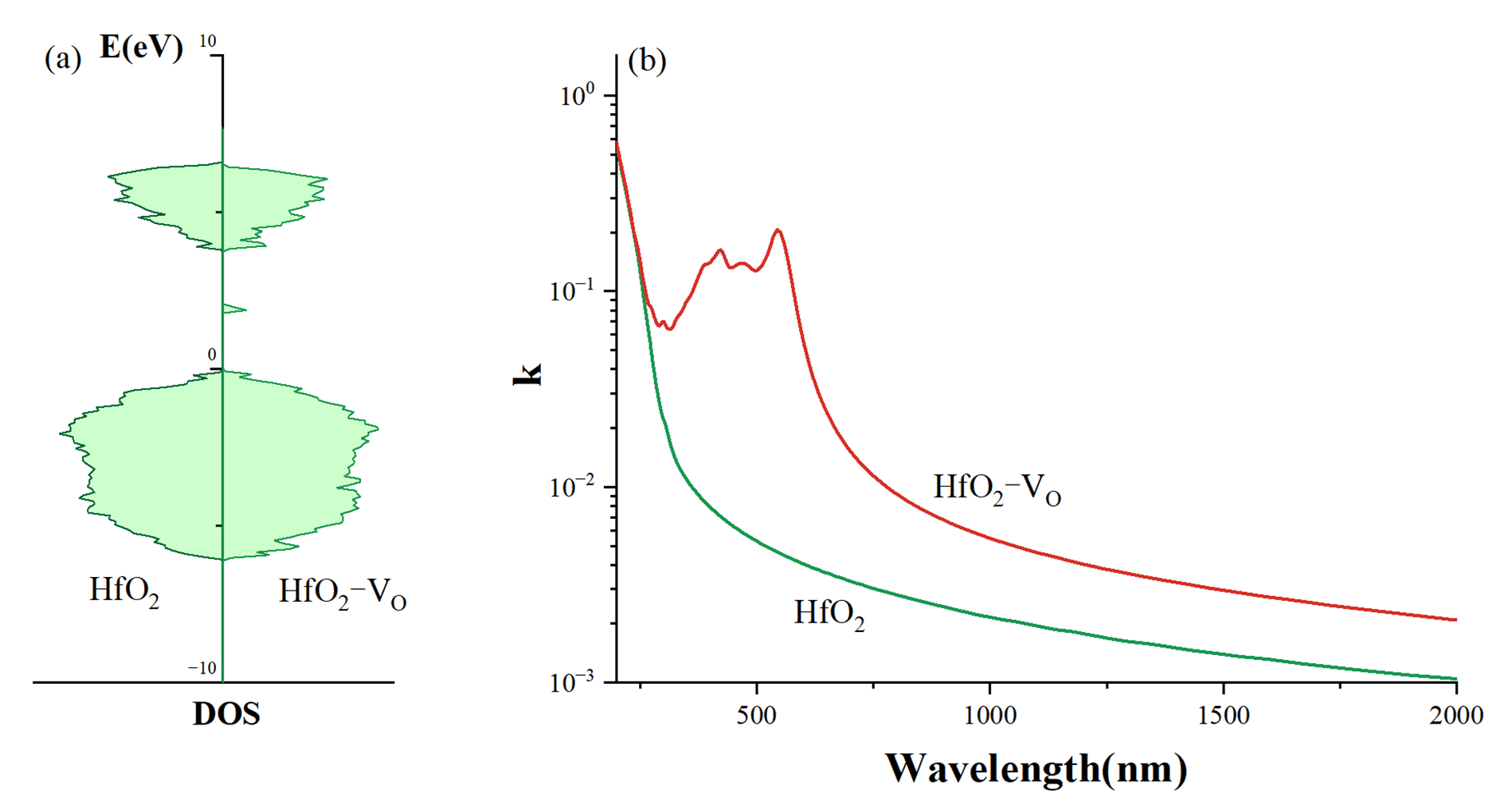
Figure 1. Density functional theory calculations were employed to investigate the electronic density of states for both the HfO
2 thin films with and without V
O, as shown in
Figure 2a. The complex dielectric constant was determined from the electronic structure calculations, and the extinction coefficients of the models were calculated using the formula:
as depicted in
Figure 2b, where
ε1 represents the real part of the dielectric constant and
ε2 represents the imaginary part.
In the absence of V
O, the extinction coefficient of the amorphous HfO
2 film demonstrates an exponential decrease in the range of 500 nm to 2000 nm. This range corresponds to photon energies lower than the bandgap width, which inhibits direct electron transitions from the valence band to the conduction band. The observed absorption in this spectral range is attributed to Urbach tail absorption arising from the intrinsic structural disorder of the amorphous phase [
32]. The distribution of bond lengths, bond angles, and local coordination variations creates localized electronic states near the band edges. This characteristic is consistent with the expected properties of an amorphous HfO
2 film.
The introduction of VO into the amorphous HfO2 structure generates additional localized energy levels deeper within the bandgap. This phenomenon results in an absorption peak around 500 nm and a notable enhancement in light absorption at 1064 nm, representing more than just a shift of the absorption tail but rather the introduction of new optically active defect states. Consequently, we propose a hypothesis: if crystallization occurs in the amorphous HfO2 film, numerous interfaces between the amorphous structures and crystalline grains will form, leading to an increase in various defects, including VO. As a result, the absorption of 1064 nm light by the film is expected to increase.
Based on the calculated results, an experiment was designed to fabricate single-layer HfO2 films to investigate the effects of VO and the presence of crystalline grains in the amorphous structure on the light absorption of HfO2 thin films at 1064 nm. Utilizing Hf metal as the source material, the deposition atmosphere was adjusted to create either an oxygen-rich or oxygen-deficient environment, resulting in highly oxidized or partially oxidized HfO2 thin films. By controlling the substrate temperature and the presence of the plasma source during the deposition processes, we regulated the microstructure of the thin films in an effort to produce HfO2 films with either a highly amorphous structure or an amorphous structure containing crystalline grains.
The transmittance curves of the samples are shown in
Figure 3a, where the black line denotes the transmittance of the quartz substrate. Small deviations where the film appears slightly more transmissive than the substrate are attributed to experimental uncertainties in baseline subtraction, slight misalignment between sample and reference measurements, and thin film interference effects. The transmittance peaks of the samples are comparable to that of the quartz substrate, with the exception of HfO
2-B, suggesting a low absorption of photons with energies below the bandgap energy. The F-B model fits the refractive index n(λ), extinction coefficient k(λ) and film thickness simultaneously from the measured transmittance data, accounting for multiple reflections at the film interfaces. The calculated film thickness was determined to be 300 ± 30 nm for the five samples, which is in good agreement with preset deposition thickness. The absorption coefficient was then calculated from the extinction coefficient using α = 4πk/λ, as depicted in
Figure 3c.
Table 2 also presents the measured absorption values of the samples at 1064 nm. With a lower oxygen flow rate during the deposition process, HfO
2-B demonstrates significantly higher absorption compared to the other samples. This indicates that HfO
2-B was not fully oxidized during deposition, generating a substantial concentration of V
O and consequently increasing the absorption coefficient.
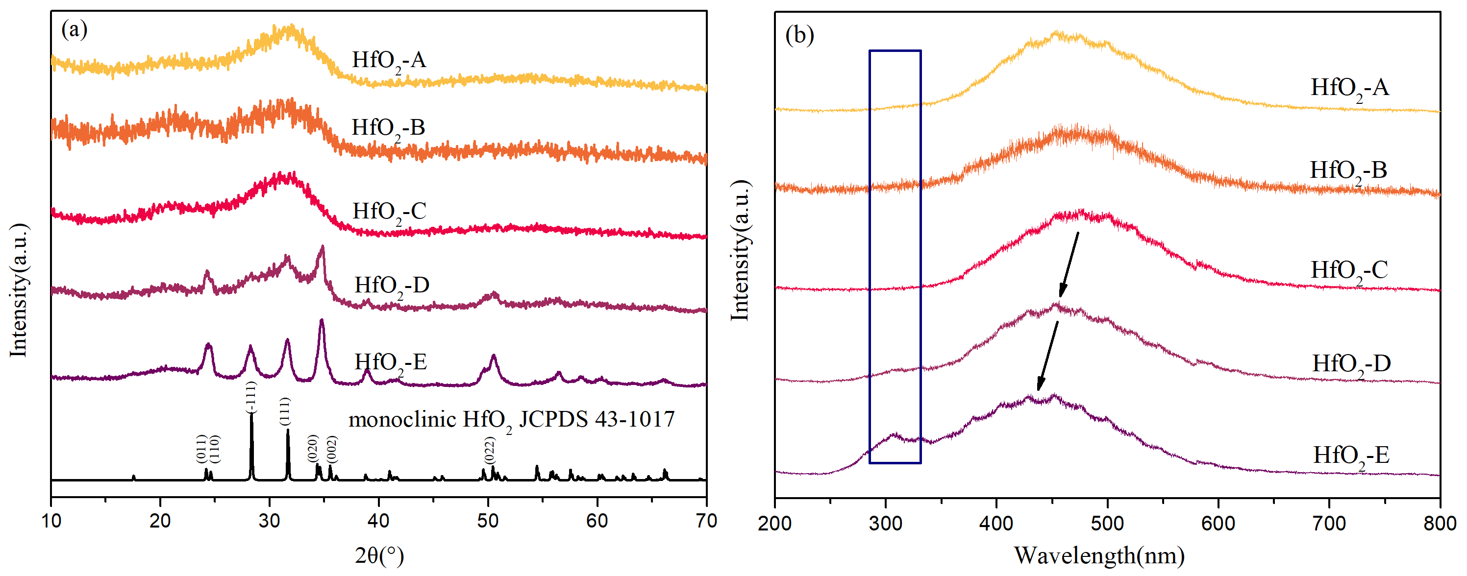
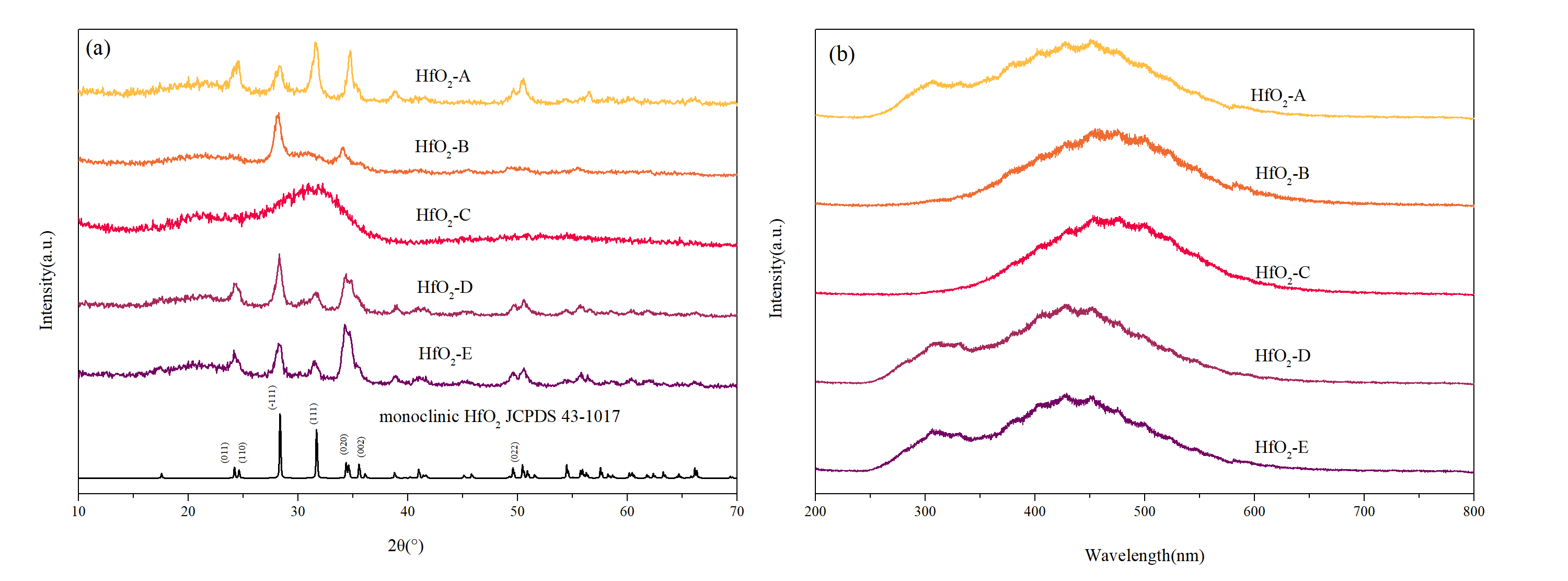
Figure 4a presents the XRD measurement results of the samples, along with the reference diffraction pattern for monoclinic HfO
2 (JCPDS 43-1017). The XRD curves of HfO
2-A, -B, and -C exhibit distinct features indicative of an amorphous structure (only broad diffuse peaks without any sharp Bragg peaks). Conversely, the XRD curves of HfO
2-D and -E not only show an amorphous structure but also present sharp diffraction peaks, indicating the presence of crystalline structures. Notably, the sharp diffraction peaks in the XRD patterns of HfO
2-D and -E align closely with the standard XRD characterization peaks of monoclinic-phase HfO
2 crystals. This suggests that during the film deposition process, a portion of the structure developed in an amorphous state while simultaneously forming monoclinic-phase HfO
2 grains.
Figure 4b illustrates the fluorescence emission spectra of the thin film samples excited by 193 nm light. An abrupt increase in fluorescence intensity around 580 nm is observed, attributed to the grating switching of the fluorescence measurement device at that specific position. The fluorescence emission spectra of HfO
2-A, -B, and -C exhibit general similarities, although the fluorescence signal of HfO
2-B is comparatively weaker, resulting in a slightly different signal-to-noise ratio. The fluorescence emission spectra of HfO
2-D and -E display distinct differences. Notably, the main peak position of HfO
2-D shifts toward shorter wavelengths compared to samples A–C, while the main peak position of HfO
2-E shifts even further toward shorter wavelengths compared to HfO
2-D. Additionally, HfO
2-D presents a weaker fluorescence emission peak around 310 nm, whereas HfO
2-E exhibits a stronger fluorescence emission peak at that position.
Analysis of the XRD curves and fluorescence emission spectra reveals that HfO2-A, -B, and -C exhibit an amorphous structure, with their fluorescence emission peak appearing as a broad peak centered around 480 nm. This broad peak may be attributed to the superposition of several fluorescence emission peaks resulting from radiative transitions of excited electrons to various lower energy levels. The crystalline grains present in HfO2-D and -E lead to the emission peak shifting toward shorter wavelengths, indicating that the monoclinic-phase HfO2 grains exhibit stronger fluorescence emission peaks at shorter wavelengths under 193 nm light excitation. As a result, these peaks overlap with the fluorescence emission peaks of the amorphous structure, leading to the observed shift toward shorter wavelengths. Furthermore, the presence of crystalline grains introduces a new fluorescence emission peak around 310 nm. The XRD curves clearly indicate higher crystallinity in HfO2-E compared to HfO2-D. Therefore, the main peak position of HfO2-E exhibits a more significant shift toward shorter wavelength, and the emission peak at 310 nm is stronger than that of HfO2-D.
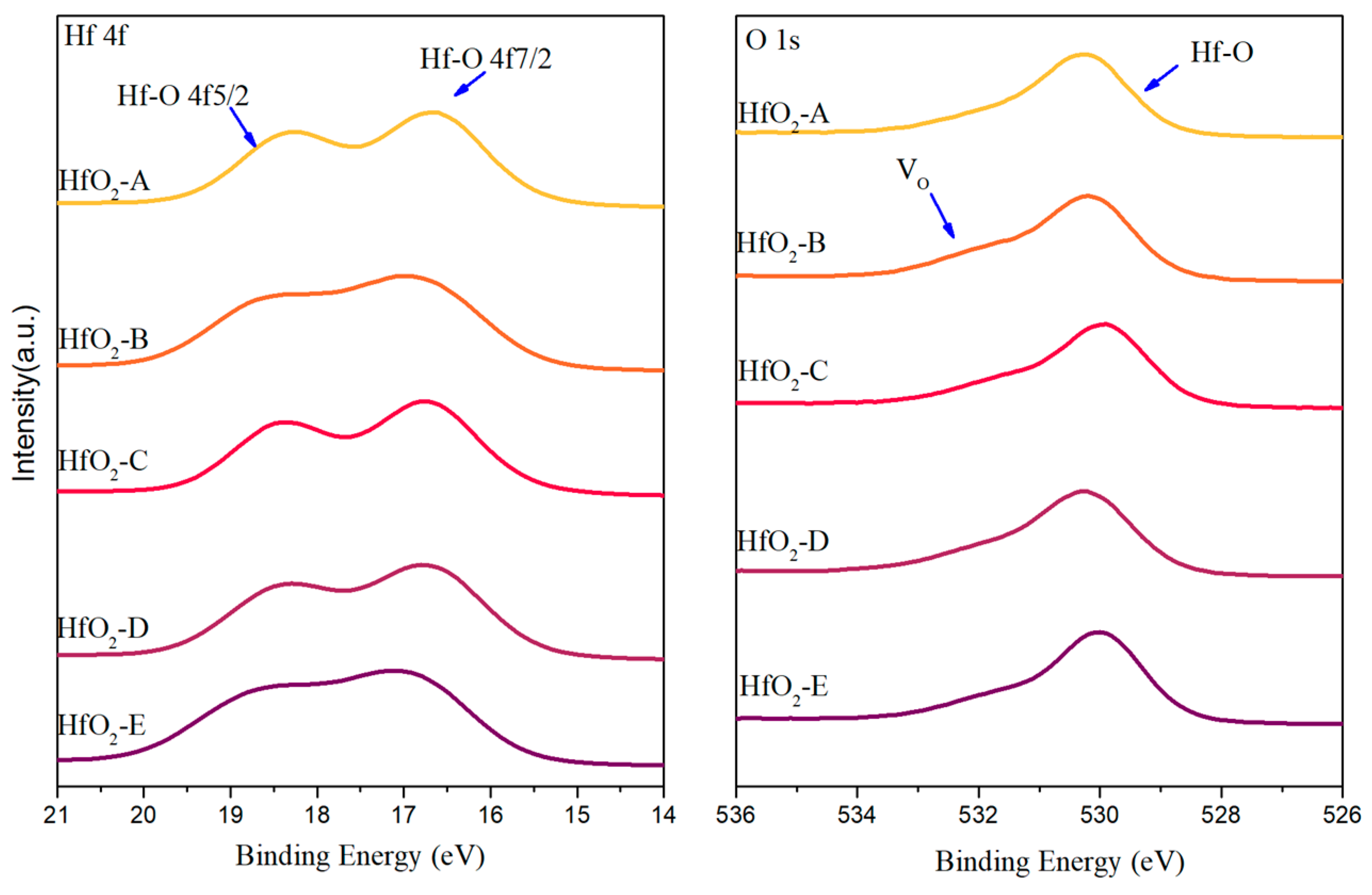
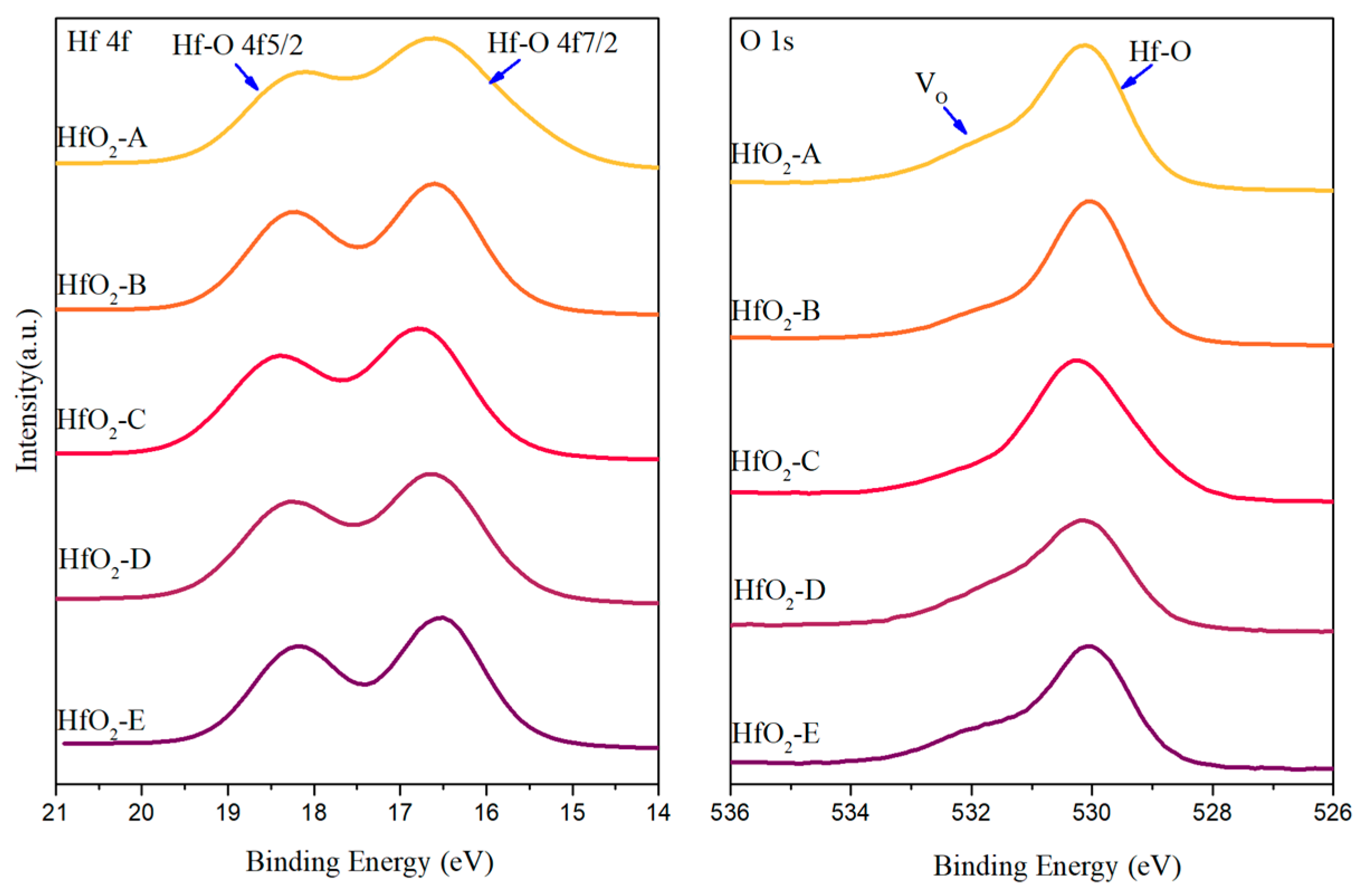
Figure 5 presents the Hf 4f and O 1s core-level spectra of the samples. The Hf 4f spectrum typically exhibits a characteristic doublet with binding energies of approximately 16.8 eV (4f7/2) and 18.5 eV (4f5/2), The as-deposited HfO
2-A, C, D samples display Hf 4f peaks that closely align with the characteristic values [
33], indicating predominantly Hf
4+ states and near-stoichiometric composition. In contrast, HfO
2-B and HfO
2-E exhibit Hf 4f peak shapes that deviate from the standard doublet pattern. This deviation suggests the presence of different oxidation states of hafnium, including Hf
3+, Hf
2+, or possibly metallic Hf
0 species, confirming that these films contain sub-stoichiometric hafnium oxide phases. The O 1s spectra provide complementary information regarding oxygen chemical environments and vacancy concentrations. The O 1s region can be deconvoluted into lattice oxygen in Hf-O bonds (centered around 530.5 eV) and V
O (centered around 532.0 eV) [
33]. HfO
2-B exhibits a significant V
O peak, corroborating the interpretation that its high optical absorption stems from substantial oxygen deficiency. Conversely, HfO
2-A and HfO
2-C display weaker V
O signals, consistent with their lower absorption values.
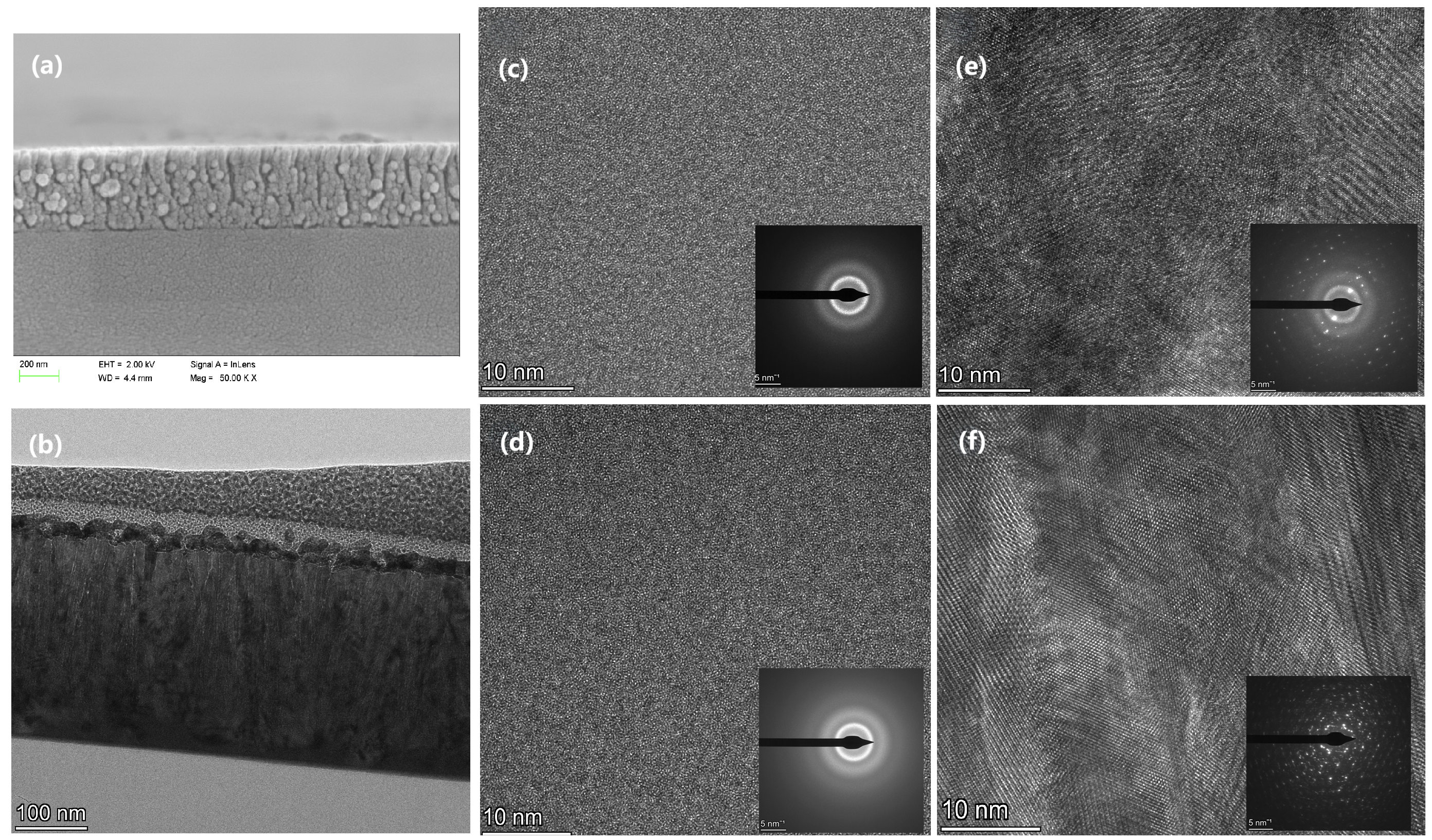
Figure 6a presents the cross-sectional SEM image of HfO
2-E, which exhibits a typical columnar structure deposited via the evaporation method. The film’s density is relatively low compared to that of the sputtering deposition method, resulting in more internal pores and a higher potential for interfaces and defects.
Figure 6b shows the TEM image of HfO
2-E after FIB slicing. The film exhibits a columnar structure, consistent with the observations in
Figure 6a.
Figure 6c presents a high-resolution TEM image and SAED of HfO
2-C after FIB slicing, confirming the absence of crystal structure, consistent with the results obtained from the XRD and fluorescence analysis. In
Figure 6e, a high-resolution TEM image and SAED of HfO
2-E reveals distinct crystal planes surrounded by amorphous structures, confirming the coexistence of amorphous structures and crystalline grains in the thin film, as indicated by the XRD and fluorescence analysis.
Moreover, despite the fact that HfO2-C has an amorphous structure and HfO2-D contains crystalline grains, the absorption of HfO2-C is only marginally lower than that of HfO2-D. Comparing the differences in the deposition parameters of the two samples, HfO2-C was deposited at a substrate temperature of 120 °C, while HfO2-D was deposited at 160 °C. This difference in temperature may lead to HfO2-D demonstrating a superior degree of oxidation during the deposition process, as it is more likely to react with oxygen at a higher substrate temperature compared to HfO2-C. Therefore, the slightly lower absorption observed in HfO2-C could be attributed to the combined effects of oxidation degree and crystallization presence.
The variation in the performance of thin films during use is crucial for understanding the mechanisms of laser damage [
34]. In many practical laser applications, HfO
2 films are typically operated in air, and they experience cumulative thermal effects during prolonged exposure to laser radiation. Initial absorption of laser energy causes localized heating of the film. When the temperature becomes sufficiently high, the amorphous structure begins to crystallize, forming crystalline grains and associated crystalline-amorphous interfaces. These interfaces introduce additional V
O defects, as demonstrated by our theoretical calculations and experimental observations. The increased defect density enhances optical absorption at 1064 nm, leading to further temperature rise and accelerated crystallization. Films experience cumulative thermal effects during prolonged exposure to laser radiation. At a certain point during operation, this effect manifests as a sudden decrease in the damage threshold compared to the initial performance, which can potentially result in catastrophic failure of the optical coating. Thermal annealing experiments at 400 °C were designed to simulate the long-term thermal stability of the films under realistic operational conditions.
After subjecting the samples to heat treatment in an air atmosphere at 400 °C, the absorption at 1064 nm, XRD curves, fluorescence emission spectra and XPS were measured again. The GIXRD curves in
Figure 7a reveal that the samples exhibit distinct crystalline states, with the exception of HfO
2-C. Among these, HfO
2-A, -D, and -E display diffraction peaks at the same positions as monoclinic-phase HfO
2 crystals. To some extent, GIXRD can characterize the preferred crystallographic orientation of polycrystalline thin films by statistically analyzing the intensity distribution of diffraction peaks from thousands of randomly oriented grains within the X-Ray illuminated area. In the case of HfO
2-B, distinct diffraction peaks corresponding to the (−111), (020), and (002) crystal planes are observed when the amorphous structure crystallizes [
35]. The appearance of these specific reflections may indicate oriented grain growth. On the other hand, HfO
2-C maintains its amorphous structure. The fluorescence emission spectra in
Figure 7b show that the main emission peaks of HfO
2-A, D, and E shift toward shorter wavelengths, along with an emission peak around 310 nm, consistent with the previous discussion regarding the emission peak positions of HfO
2 thin films with a crystalline structure. The fluorescence behavior of HfO
2-B after annealing (
Figure 7b) presents an interesting anomaly. Despite undergoing crystallization, its emission spectrum resembles that of amorphous samples rather than showing the characteristic features of crystalline HfO
2 (such as the 310 nm peak observed in HfO
2-D and HfO
2-E). This suggests that annealed HfO
2-B does not significantly increase the intensity of the emission peak at shorter wavelengths and does not generate a fluorescence emission peak at 310 nm. This phenomenon may result from symmetry breaking induced by oriented growth, which could lead to selectively forbidden transitions in the fluorescence emissions observed in other crystallized samples. This observation may indicate that oriented grain growth occurred in HfO
2-B after annealing, which is consistent with the GIXRD analysis discussed above.
The absorption characteristics of the samples were modified following heat treatment, as shown in
Table 2. HfO
2-A, -D, and -E demonstrated increased absorption, while HfO
2-B and -C exhibited decreased absorption. Analysis of the XRD curves and fluorescence emission spectra suggests that heat treatment at 400 °C enhanced crystallinity and introduced additional defect structures in HfO
2-A, -D, and -E, leading to increased absorption. Despite the presence of crystallization in HfO
2-B after heat treatment, its absorption decreased significantly from the original 913.2 ppm to 29.3 ppm. This reduction is attributed to the film being deposited in an oxygen-deficient atmosphere and subsequently reacting with atmospheric oxygen during the heat treatment, effectively compensating for the oxygen-deficient defects within the film. Consequently, despite the formation of the crystalline states, HfO
2-B experienced a considerable decrease in absorption. HfO
2-C maintained a well-preserved amorphous structure even after heat treatment, with absorption decreasing from 12.1 ppm to 9.3 ppm. This decrease is attributed to further oxidation, which aligns with the previous discussion that the relatively low substrate temperature during the deposition of HfO
2-C may have resulted in insufficient oxidation.
Following heat treatment at 400 °C in air, notable changes occur in the XPS spectra (
Figure 8). The Hf 4f spectra of all samples converge toward the characteristic doublet pattern of Hf
4+. For HfO
2-B, the V
O peak intensity decreases substantially, confirming that the dramatic reduction in optical absorption (from 913.2 ppm to 29.3 ppm) results from re-oxidation that compensates for the initial oxygen deficiency. This re-oxidation effect outweighs the defect generation associated with the crystallization observed in XRD. Conversely, HfO
2-A shows a marked increase in the V
O peak after annealing, correlating with its increased optical absorption (from 4.5 ppm to 80.5 ppm). This behavior aligns with our hypothesis that crystallization of initially amorphous films generates new interfacial defects and V
O at the boundaries between crystalline grains and residual amorphous regions. HfO
2-C maintains relatively low V
O signals both before and after annealing, consistent with its preserved amorphous structure and low absorption.
The exceptional stability of the amorphous phase in sample HfO2-C after 400 °C annealing arises from synergistic effects of the deposition conditions. Plasma assistance during deposition creates a denser, more homogeneous amorphous network with fewer nucleation sites for crystallization. The lower substrate temperature (120 °C) reduces atomic mobility during growth, resulting in a more relaxed amorphous structure that is further from the crystallization threshold. The combination of plasma-induced densification and low temperature deposition effectively suppresses the crystallization process even under prolonged thermal treatment.
In conclusion, HfO2-C exhibits low light absorption and maintains a well-preserved amorphous structure after heat treatment at 400 °C, with a slight decrease in absorption. This characteristic effectively mitigates performance degradation of the thin film in extreme high-temperature environments and during prolonged operation, enhancing resistance to laser damage and extending service life under practical working conditions.
