
Early Periods of Low-Temperature Linear Antenna CVD Nucleation and Growth Study of Nanocrystalline Diamond Films


Abstract
1. Introduction
2. Materials and Methods
2.1. Substrates
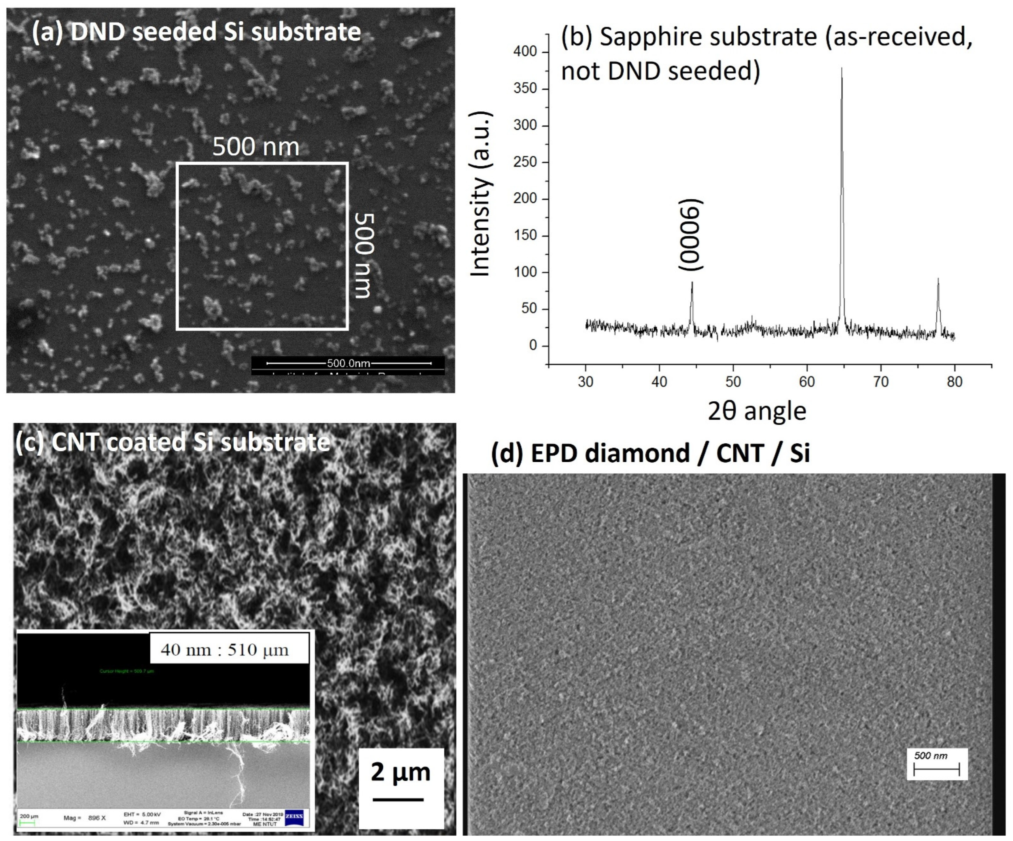
2.1.1. DND Seeding
2.1.2. CNT and EPD
2.2. LA-MPCVD
2.3. Physical Characterisations
3. Results and Discussion
3.1. First Hour of LA-MPCVD Growth
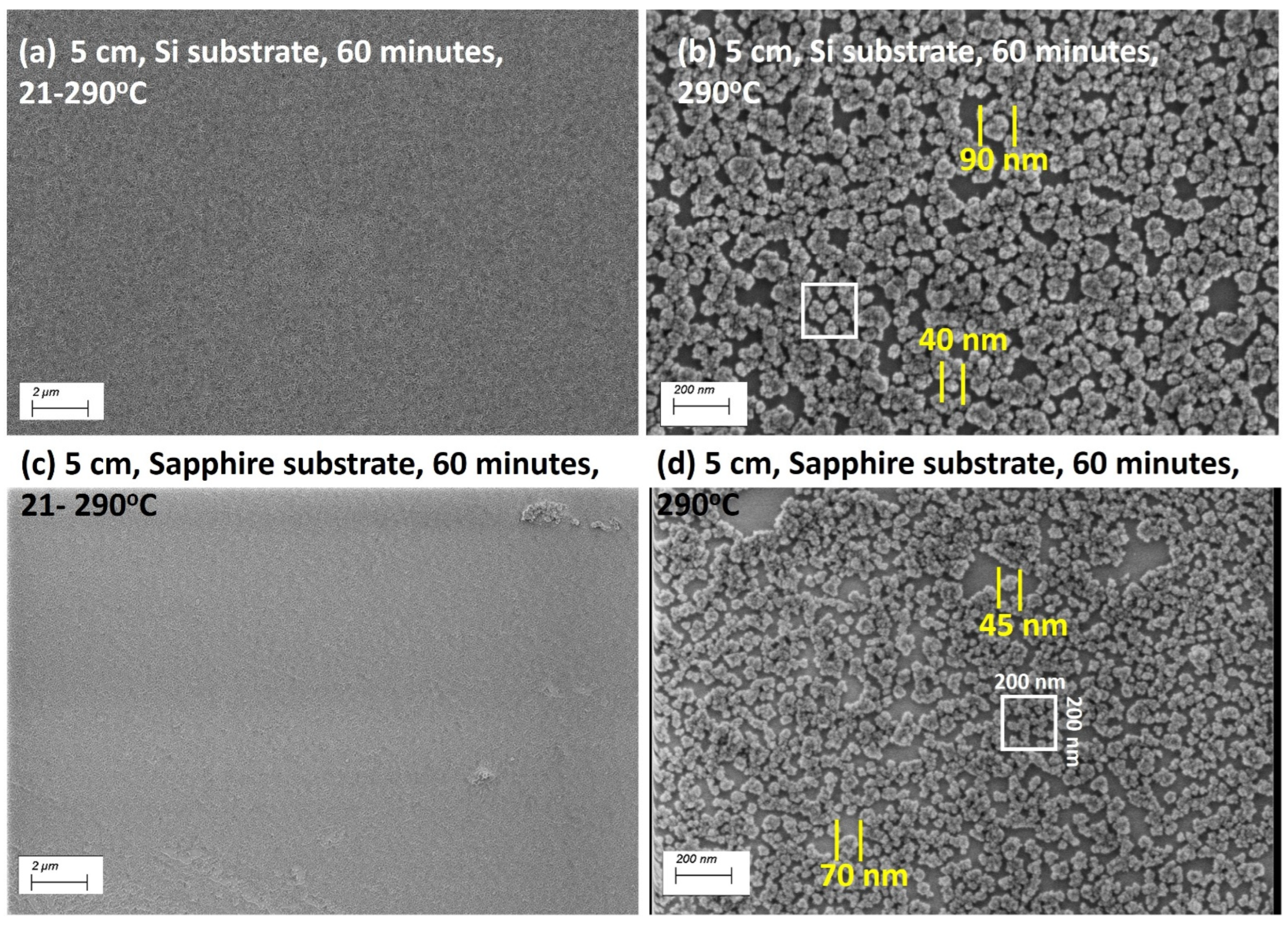
3.1.1. Silicon Substrates
3.1.2. Sapphire Substrates
3.1.3. CNT and EPD Substrates
3.2. Low MW Power
3.3. Pulse Mode MW Power
3.4. Fully Coalesced NCD Films
3.5. LA-MPCVD Growth without CO2
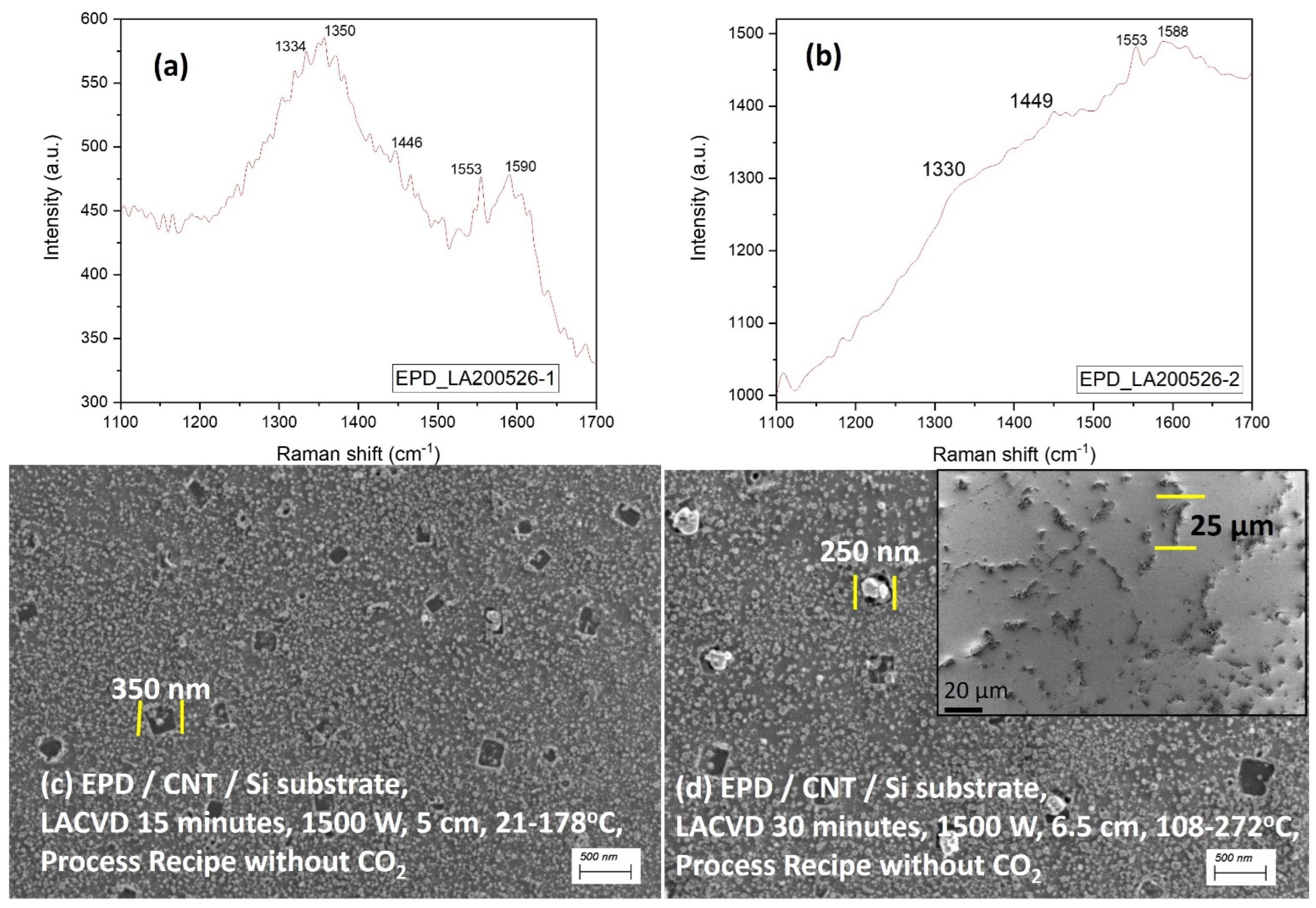
3.5.1. EPD-Diamond/CNT/Si Substrates
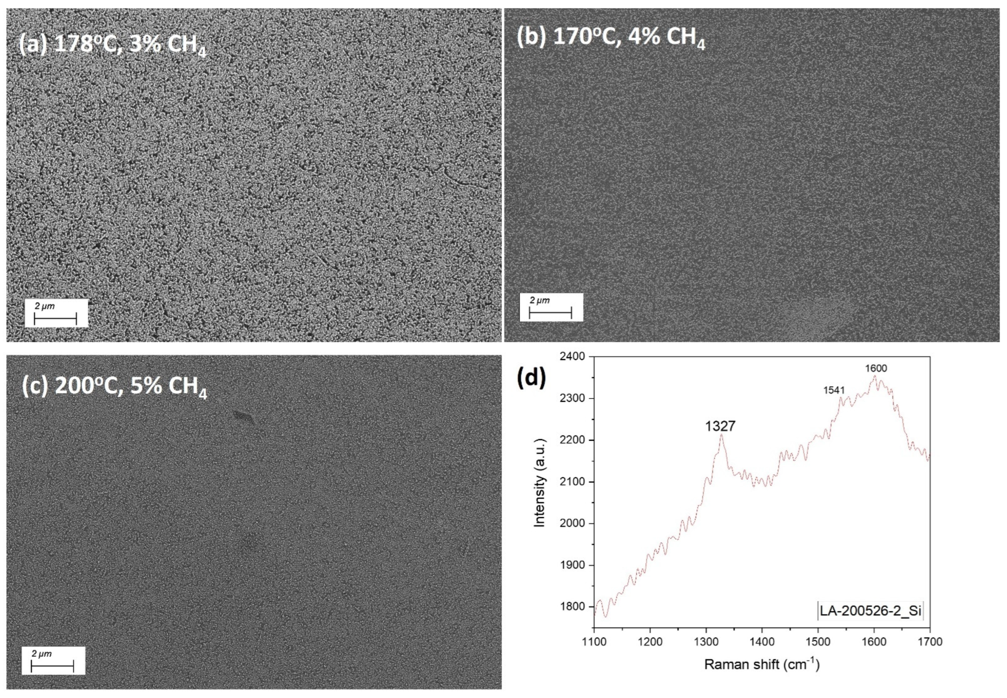
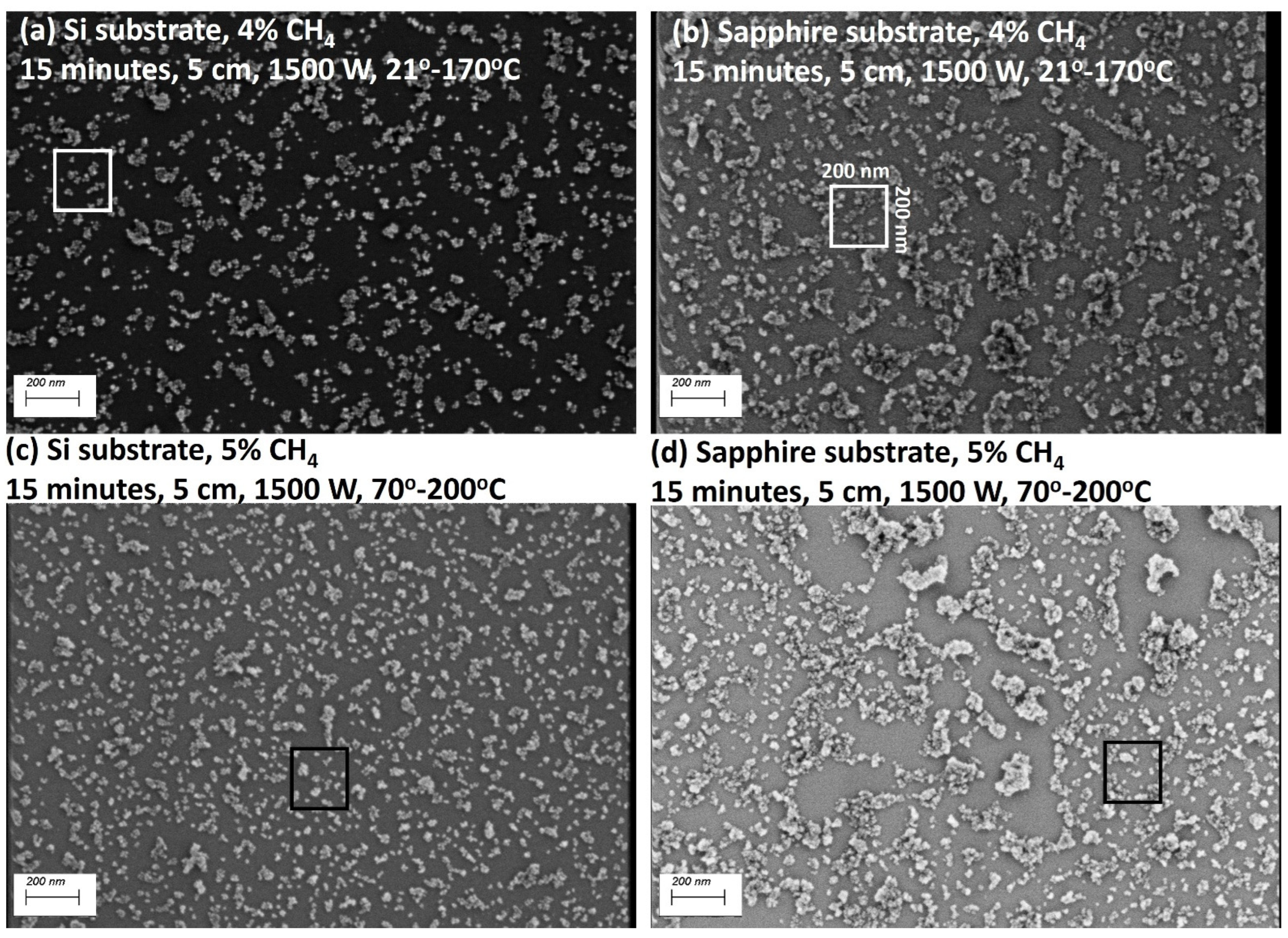
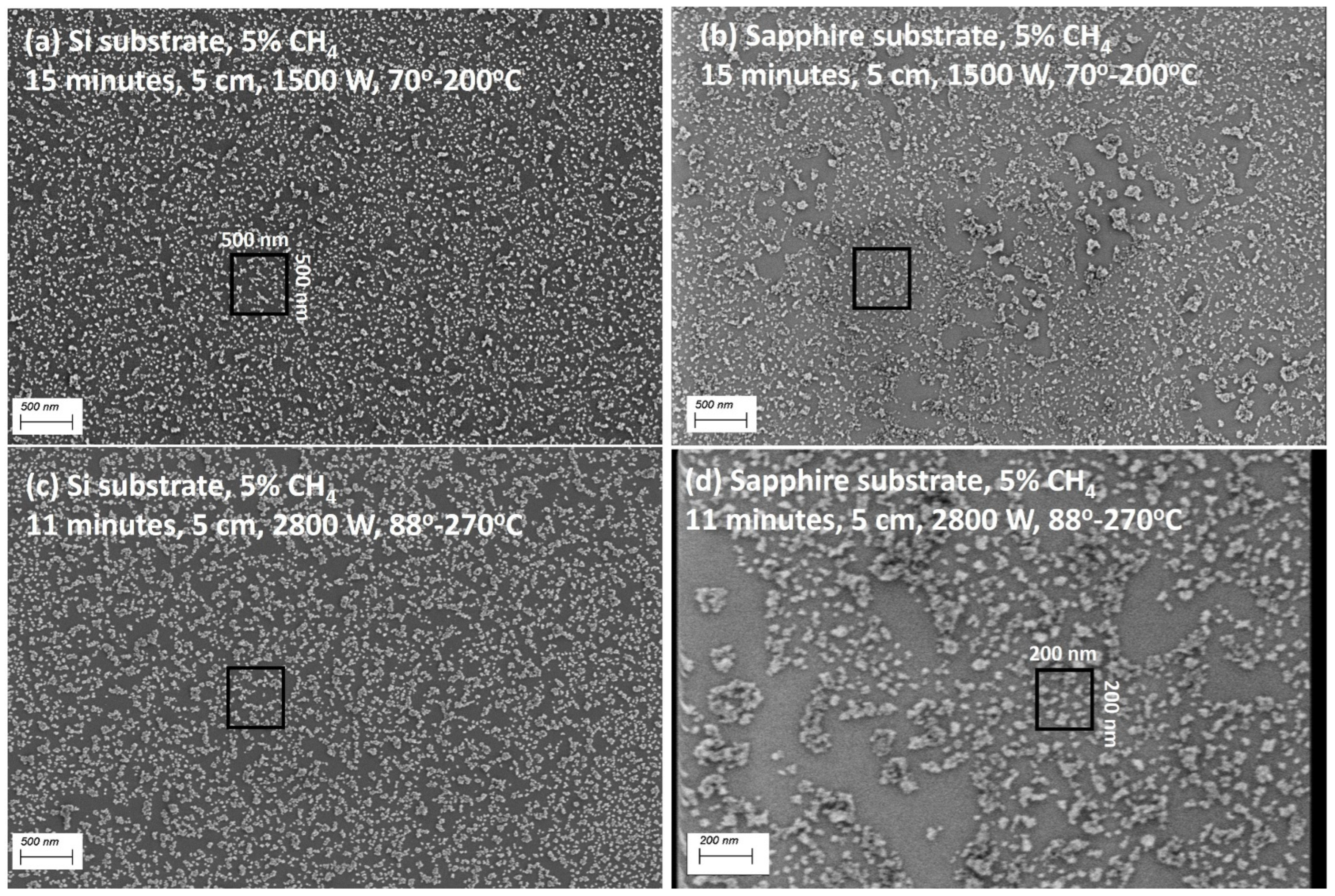
3.5.2. Silicon and Sapphire Substrates
Effect of CH4
Effect of Deposition Time
4. Conclusions
- (a)
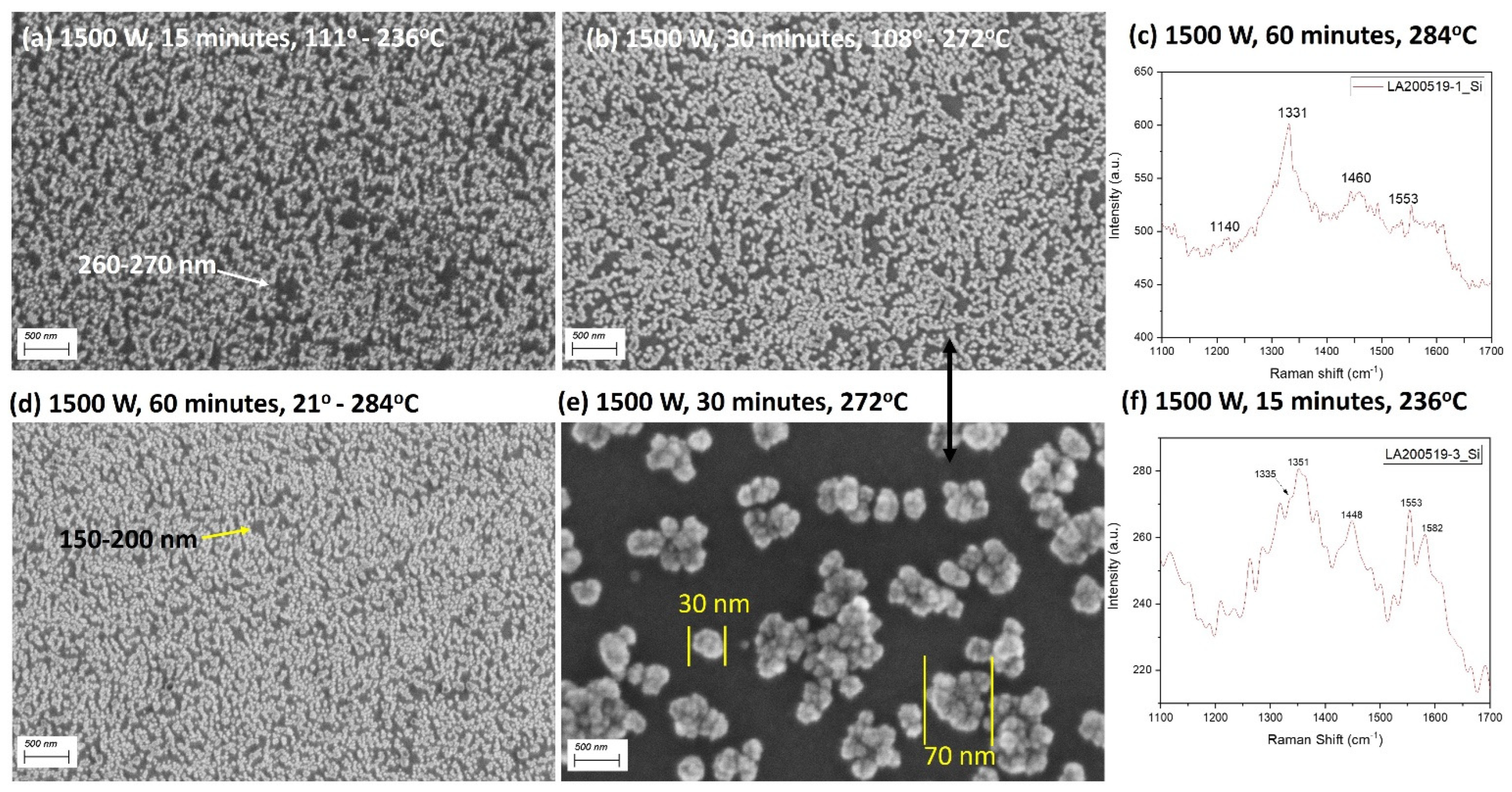
- The substrate temperature keeps increasing during the first hours of LA-MPCVD and the NCD film remains discontinuous on the DND-seeded silicon and sapphire substrates.
- (b)
- The short duration LA-MPCVD runs for 15 min were not effective in coalescing the NCD films, but they were found to be appropriate for coating CNTs with NCDs.
- (c)
- The CNT/Si samples were found to be severely etched out under a H2/CH4/CO2 = 89/5/6 plasma recipe—more than the EPD-treated CNT/Si substrates. Pre-treatment with electrophoretic diamond seeds helped in protecting the carbon nanotubes from plasma etching, as evident from their longer CNT lengths after 15 min of LA-MPCVD runs.
- (d)
- Further prevention of plasma etching of the EPD-seeded CNT/Si substrate was observed without CO2 gas in the LA-MPCVD process recipe, with evidence of 25 µm long CNTs present even after 30 min of LA-MPCVD runs.
- (e)
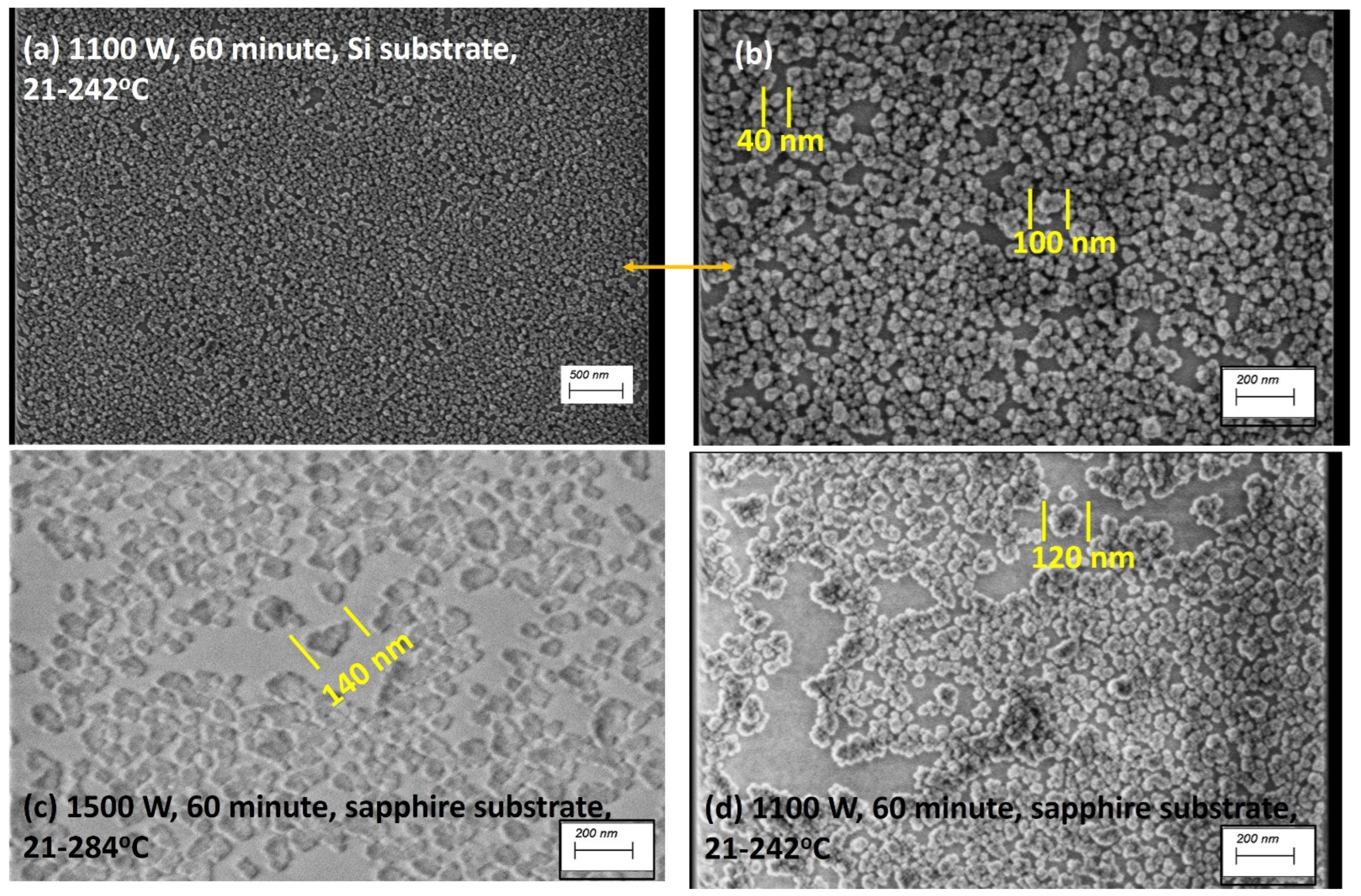
- DND-seeded sapphire substrates were found to favor the formation of bigger and denser NCD particles than the silicon substrates. Moreover, the Raman signals were also found to be relatively better from sapphire substrates (FWHM of sp3 = 15 cm−1) than from the NCDs on silicon substrate, under identical LA-MPCVD parameters.
- (f)
- Lowering of the input microwave power level from 1500 to 1100 W in continuous wave mode favored the formation of connected NCDs.
- (g)
- On the other hand, pulse mode LA-MPCVD experiments were also found to help in improving NCD crystal formation with bigger grain sizes (40–90 nm on Si) and more effective surface coverage of the substrates.
- (h)
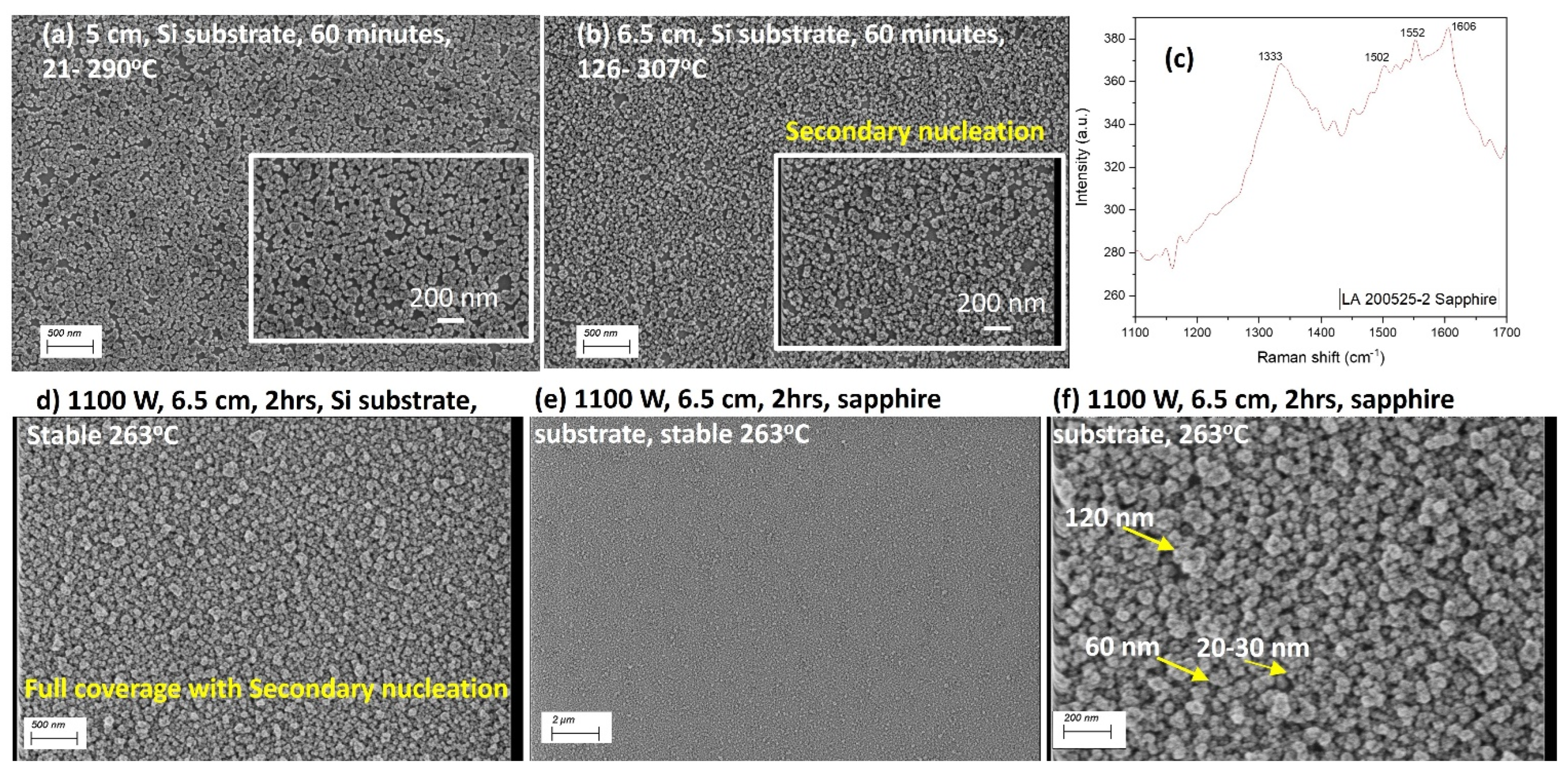
- Increasing the stage-to-antenna distance from 5 cm to 6.5 cm promoted the formation of secondary nucleation sites. Re-nucleation at longer substrate-to-quartz-tube distances, along with a longer deposition time of 2 h, are found to be essential in growing continuous NCD films.
- (i)
- The effect of increasing CH4 percentages in the process recipe was to supply more carbon atoms necessary for increasing the densities of diamond nanoparticles on DND-seeded substrates.
- (j)
- Deposition time is the most important factor for NCD growth during the early stages of LA-MPCVD. Even a higher input power of 2800 W (and therefore higher temperatures) could not significantly affect the NCD crystal sizes within short periods of time.
- (k)
- It was necessary to run the LA-MPCVD experiments for long enough (2 h) to achieve a flat stable substrate temperature (263 °C).
Author Contributions
Funding
Institutional Review Board Statement
Informed Consent Statement
Data Availability Statement
Acknowledgments
Conflicts of Interest
References
- Grotjohn, T.A.; Asmussen, J. Microwave Plasma-Assisted Diamond Film Deposition. In Diamond Films Handbook; Asmussen, J., Reinhard, D.K., Eds.; Marcel Dekker, Inc.: New York, NY, USA, 2002; Chapter 7. [Google Scholar]
- Das, D.; Singh, R.N. A review of nucleation, growth and low temperature synthesis of diamond thin films. Int. Mater. Rev. 2007, 52, 29–64. [Google Scholar] [CrossRef]
- Piazza, F.; Morell, G. Synthesis of diamond at sub 300 °C substrate temperature. Diam. Relat. Mater. 2007, 16, 1950–1957. [Google Scholar] [CrossRef]
- Ihara, M.; Maeno, H.; Miyamoto, K.; Komiyama, H. Low-temperature deposition of diamond in a temperature range from 70 °C to 700 °C. Diam. Relat. Mater. 1992, 1, 187–190. [Google Scholar] [CrossRef]
- Potocky, S.; Kromka, A.; Potmesil, J.; Remes, Z.; Polackova, Z.; Vanecek, M. Growth of nanocrystalline diamond films deposited by microwave plasma CVD system at low substrate temperatures. Phys. Status Solidi 2006, 203, 3011–3015. [Google Scholar] [CrossRef]
- Gueroudji, L.; Hwang, N.M. Thermodynamic limits for the substrate temperature in the CVD diamond process. Diam. Relat. Mater. 2000, 9, 205–211. [Google Scholar] [CrossRef]
- Gu, J.; Chen, Z.; Li, R.; Zhao, X.; Das, C.; Sahmuganathan, V.; Sudijono, J.; Lin, M.; Loh, K.P. Nanocrystalline diamond film grown by pulsed linear antenna microwave CVD. Diam. Relat. Mater. 2021, 119, 108576. [Google Scholar] [CrossRef]
- Tsugawa, K.; Ishihara, M.; Kim, J.; Hasegawa, M.; Koga, Y. Large-Area and Low-Temperature Nanodiamond Coating by Microwave Plasma Chemical Vapor Deposition. New Diam. Front. Carbon Technol. 2006, 16, 337–346. [Google Scholar]
- Marton, M.; Vojs, M.; Michniak, P.; Behúl, M.; Rehacek, V.; Pifko, M.; Stehlík, S.; Kromka, A. New chemical pathway for large-area deposition of doped diamond films by linear antenna microwave plasma chemical vapor deposition. Diam. Relat. Mater. 2022, 126, 109111. [Google Scholar] [CrossRef]
- Kromka, A.; Babchenko, O.; Izak, T.; Hruska, K.; Rezek, B. Linear antenna microwave plasma CVD deposition of diamond films over large areas. Vacuum 2012, 86, 776–779. [Google Scholar] [CrossRef]
- Fendrych, F.; Taylor, A.; Peksa, L.; Kratochvilova, I.; Vlcek, J.; Rezacova, V.; Petrak, V.; Kluiber, Z.; Fekete, L.; Liehr, M.; et al. Growth and characterization of nanodiamond layers prepared using the plasma-enhanced linear antennas microwave CVD system. J. Phys. D Appl. Phys. 2010, 43, 374018. [Google Scholar] [CrossRef]
- Potocký, Š.; Babchenko, O.; Hruška, K.; Kromka, A. Linear antenna microwave plasma CVD diamond deposition at the edge of no-growth region of C-H-O ternary diagram. Phys. Status Solidi 2012, 249, 2612–2615. [Google Scholar] [CrossRef]
- Taylor, A.; Fendrych, F.; Fekete, L.; Vlček, J.; Řezáčová, V.; Petrák, V.; Krucký, J.; Nesládek, M.; Liehr, M. Novel high frequency pulsed MW-linear antenna plasma-chemistry: Routes towards large area, low pressure nanodiamond growth. Diam. Relat. Mater. 2011, 20, 613–615. [Google Scholar] [CrossRef]
- Izak, T.; Babchenko, O.; Varga, M.; Potocky, S.; Kromka, A. Low temperature diamond growth by linear antenna plasma CVD over large area. Phys. Status Solidi 2012, 249, 2600–2603. [Google Scholar] [CrossRef]
- Drijkoningen, S.; Pobedinskas, P.; Korneychuk, S.; Momot, A.; Balasubramaniam, Y.; Van Bael, M.K.; Turner, S.; Verbeeck, J.; Nesla, M.; Haenen, K. On the Origin of Diamond Plates Deposited at Low Temperature. Cryst. Growth Des. 2017, 17, 4306–4314. [Google Scholar] [CrossRef]
- Mistrik, J.; Janicek, P.; Taylor, A.; Fendrych, F.; Fekete, L.; Jager, A.; Nesladek, M. Spectroscopic ellipsometry characterization of nano-crystalline diamond films prepared at various substrate temperatures and pulsed plasma frequencies using microwave plasma enhanced chemical vapor deposition apparatus with linear antenna delivery. Thin Solid Films 2014, 571, 230–237. [Google Scholar] [CrossRef]
- Tsugawa, K.; Ishihara, M.; Kim, J.; Koga, Y.; Hasegawa, M. Nanocrystalline diamond film growth on plastic substrates at tem-peratures below 100 °C from low-temperature plasma. Phys. Rev. B 2010, 82, 125460. [Google Scholar] [CrossRef]
- Neykova, N.; Kozak, H.; Ledinsky, M.; Kromka, A. Novel plasma treatment in linear antenna microwave PECVD system. Vacuum 2012, 86, 603–607. [Google Scholar] [CrossRef]
- Bénédic, F.; Belmahi, M.; Easwarakhanthan, T.; Alnot, P. In situ optical characterization during MPACVD diamond film growth on silicon substrates using a bichromatic infrared pyrometer under oblique incidence. J. Phys. D Appl. Phys. 2001, 34, 1048. [Google Scholar] [CrossRef]
- Gracio, J.J.; Fan, Q.H.; Madaleno, J.C. Diamond growth by chemical vapour deposition. J. Phys. D Appl. Phys. 2010, 43, 374017. [Google Scholar] [CrossRef]
- Kromka, A.; Potocký, Š.; Čermák, J.; Rezek, B.; Potměšil, J.; Zemek, J.; Vaněček, M. Early stage of diamond growth at low tem-perature. Diam. Relat. Mater. 2008, 17, 1252–1255. [Google Scholar] [CrossRef]
- Babchenko, O.; Potocký, Š.; Ižák, T.; Hruška, K.; Bryknar, Z.; Kromka, A. Influence of surface wave plasma deposition conditions on diamond growth regime. Surf. Coat. Technol. 2015, 271, 74–79. [Google Scholar] [CrossRef]
- Bai, T.; Wang, Y.; Feygelson, T.I.; Tadjer, M.J.; Hobart, K.D.; Hines, N.J.; Yates, L.; Graham, S.; Anaya, J.; Kuball, M.; et al. Diamond Seed Size and the Impact on Chemical Vapor Deposition Diamond Thin Film Properties. ECS J. Solid State Sci. Technol. 2020, 9, 053002. [Google Scholar] [CrossRef]
- Pobedinskas, P.; Janssens, S.D.; Hernando, J.; Wagnera, P.; Nesládek, M.; Haenen, K. Selective seeding and growth of nano-crystalline CVD diamond on non-diamond substrates. MRS Proc. 2011, 1339, 1–6. [Google Scholar] [CrossRef]
- Pobedinskas, P.; Degutis, G.; Dexters, W.; Janssen, W.; Janssens, S.D.; Conings, B.; Ruttens, B.; D’Haen, J.; Boyen, H.-G.; Hardy, A.; et al. Surface plasma pretreatment for enhanced diamond nucleation on AlN. Appl. Phys. Lett. 2013, 102, 201609. [Google Scholar] [CrossRef]
- Rotter, S.Z.; Madaleno, J.C. Diamond CVD by a Combined Plasma Pretreatment and Seeding Procedure. Chem. Vap. Depos. 2009, 15, 209–216. [Google Scholar] [CrossRef]
- Tsugawa, K.; Ishihara, M.; Kim, J.; Koga, Y.; Hasegawa, M. Nucleation Enhancement of Nanocrystalline Diamond Growth at Low Substrate Temperatures by Adamantane Seeding. J. Phys. Chem. C 2010, 114, 3822–3824. [Google Scholar] [CrossRef]
- Arnault, J.C.; Demuynck, L.; Speisser, C.; Normand, F.L. Mechanisms of CVD diamond nucleation and growth on mechanically scratched Si(100) surfaces. Eur. Phys. J. B Condens. Matter Complex Syst. 1999, 11, 327–343. [Google Scholar] [CrossRef]
- Buijnsters, J.; Vázquez, L.; ter Meulen, J. Substrate pre-treatment by ultrasonication with diamond powder mixtures for nucleation enhancement in diamond film growth. Diam. Relat. Mater. 2009, 18, 1239–1246. [Google Scholar] [CrossRef]
- Shenderova, O.; Hens, S.; McGuire, G. Seeding slurries based on detonation nanodiamond in DMSO. Diam. Relat. Mater. 2010, 19, 260–267. [Google Scholar] [CrossRef]
- Domonkos, M.; Ižák, T.; Varga, M.; Potocký, Š.; Demo, P.; Kromka, A. Diamond nucleation and growth on horizontally and vertically aligned Si substrates at low pressure in a linear antenna microwave plasma system. Diam. Relat. Mater. 2018, 82, 41–49. [Google Scholar] [CrossRef]
- Affoune, A.M.; Prasad, B.L.V.; Sato, H.; Enoki, T. Electrophoretic Deposition of Nanosized Diamond Particles. Langmuir 2001, 17, 547–551. [Google Scholar] [CrossRef]
- Tsubota, T.; Ida, S.; Okada, N.; Nagata, M.; Matsumoto, Y.; Yatsushiro, N. CVD diamond coating on WC–Co cutting tool using ECR MPCVD apparatus via electrophoretic seeding pretreatment. Surf. Coat. Technol. 2003, 169–170, 262–265. [Google Scholar] [CrossRef]
- Chang, T.-H.; Panda, K.; Panigrahi, B.K.; Lou, S.-C.; Chen, C.; Chan, H.-C.; Lin, I.-N.; Tai, N.-H. Electrophoresis of Nanodiamond on the Growth of Ultrananocrystalline Diamond Films on Silicon Nanowires and the Enhancement of the Electron Field Emission Properties. J. Phys. Chem. C 2012, 116, 19867–19876. [Google Scholar] [CrossRef]
- Smith, E.; Piracha, A.; Field, D.; Pomeroy, J.; Mackenzie, G.; Abdallah, Z.; Massabuau, F.-P.; Hinz, A.; Wallis, D.; Oliver, R.; et al. Mixed-size diamond seeding for low-thermal-barrier growth of CVD diamond onto GaN and AlN. Carbon 2020, 167, 620–626. [Google Scholar] [CrossRef]
- Potocký, Š.; Čada, M.; Babchenko, O.; Ižák, T.; Davydova, M.; Kromka, A. Perspectives of linear antenna microwave system for growth of various carbon nano-forms and its plasma study. Phys. Status Solidi 2013, 250, 2723–2726. [Google Scholar] [CrossRef]
- Potocký, Š.; Babchenko, O.; Davydova, M.; Izak, T.; Čada, M.; Kromka, A. Growth of carbon allotropes and plasma characteri-zation in linear antenna microwave plasma CVD system. Jpn. J. Appl. Phys. 2014, 53, 05FP04. [Google Scholar] [CrossRef]
- Zou, Y.; May, P.W.; Vieira, S.M.C.; Fox, N.A. Field Emission from Diamond-Coated Multiwalled Carbon Nanotube “Teepee” Structures. J. Appl. Phys. 2012, 112, 044903. [Google Scholar] [CrossRef]
- Chang, T.; Kunuku, S.; Hong, Y.; Leou, K.; Yew, T.; Tai, N.; Lin, I. Enhancement of the Stability of Electron Field Emission Behavior and the Related Microplasma Devices of Carbon Nanotubes by Coating Diamond Films. ACS Appl. Mater. Interfaces 2014, 6, 11589–11597. [Google Scholar] [CrossRef]
- Fiori, A.; Orlanducci, S.; Sessa, V.; Tamburri, E.; Toschi, F.; Terranova, M.L.; Ciorba, A.; Rossi, M.; Lucci, M.; Barnard, A.S. Hybrid Carbon Nanotube/Nanodiamond Structures as Electron Emitters for Cold Cathodes. J. Nanosci. Nanotechnol. 2008, 8, 1989–1993. [Google Scholar] [CrossRef]
- Williams, O.A.; Douheret, O.; Daenen, M.; Haenen, K.; Osawa, E.; Takahashi, M. Enhanced diamond nucleation on monodis-persed nanocrystalline diamond. Chem. Phys. Lett. 2007, 445, 255–258. [Google Scholar] [CrossRef]
- Hu, L.; Guo, Y.; Du, S.; Tian, S.; Li, J.; Gu, C. Probing trans-polyacetylene segments in a diamond film by tip-enhanced Raman spectroscopy. Diam. Relat. Mater. 2021, 116, 108415. [Google Scholar] [CrossRef]
- Tsugawa, K.; Kawaki, S.; Ishihara, M.; Kim, J.; Koga, Y.; Sakakita, H.; Koguchi, H.; Hasegawa, M. Nanocrystalline diamond growth in a surface-wave plasma. Diam. Relat. Mater. 2011, 20, 833–838. [Google Scholar] [CrossRef]
- Taylor, A.; Ashcheulov, P.; Čada, M.; Fekete, L.; Hubík, P.; Klimša, L.; Olejníček, J.; Remeš, Z.; Jirka, I.; Janíček, P.; et al. Effect of plasma composition on nanocrystalline diamond layers deposited by a microwave linear antenna plasma-enhanced chemical vapour deposition system. Phys. Status Solidi 2015, 212, 2418–2423. [Google Scholar] [CrossRef]
- Mallik, A.K.; Bysakh, S.; Sreemany, M.; Roy, S.; Ghosh, J.; Roy, S.; Mendes, J.C.; Gracio, J.; Datta, S. Property mapping of pol-ycrystalline diamond coatings over large area. J. Adv. Ceram. 2014, 3, 56–70. [Google Scholar] [CrossRef]
- Mallik, A.K.; Lloret, F.; Gutierrez, M.; Rouzbahani, R.; Pobedinskas, P.; Shih, W.C.; Haenen, K. Deposition and Characterisation of a Diamond/Ti/Diamond Multilayer Structure. Coatings 2023, 13, 1914. [Google Scholar] [CrossRef]


| Sample id | Time (min.) | Substrate Temperature (°C) | Heating Rate (°C/min) | NCD Growth Size (nm) | H2/CH4/CO2 (%) | MW Power (W) | Pulse Mode (Frequency, Duty Cycle) | Quartz-Tube-to-Substrate Distance (cm) |
|---|---|---|---|---|---|---|---|---|
| LA200519-1 | 60 | 21–284 | 4.4 | 140 (sapphire) | 89/5/6 | 1500 | NO | 5 |
| LA200519-2 | 30 | 108–272 | 5.5 | 30–70 (silicon) | ||||
| LA200519-3 | 15 | 111–236 | 8.3 | - | ||||
| LA200520-1 | 60 | 21–242 | 3.7 | 120 (sapphire) | 1100 | 5 | ||
| LA200520-2 | 120 | Stable 263 | - | 20–120 (sapphire) | 6.5 | |||
| LA200525-1 | 60 | 21–290 | 4.5 | 45–70 (sapphire) 40–90 (silicon) | 300 input/2000 output | YES, 20 kHz, 45% | 5 | |
| LA200525-2 | 126–307 | 3 | 10–100 (silicon) | 6.5 | ||||
| LA200526-1 | 15 | 21–178 | 10.5 | 30 (silicon) 20–60 (sapphire) | 97/3/0 | 1500 | NO | 5 |
| LA200526-2 | 30 | 108–272 | 5.5 | 45 (silicon) 25–100 (sapphire) | 6.5 | |||
| LA200605-1 | 15 | 21–170 | 9.9 | - | 96/4/0 | 5 | ||
| LA200605-2 | 70–200 | 8.6 | - | 95/5/0 | ||||
| LA200605-3 | 11 | 88–270 | 16.5 | - | 2800 |
Disclaimer/Publisher’s Note: The statements, opinions and data contained in all publications are solely those of the individual author(s) and contributor(s) and not of MDPI and/or the editor(s). MDPI and/or the editor(s) disclaim responsibility for any injury to people or property resulting from any ideas, methods, instructions or products referred to in the content. |
© 2024 by the authors. Licensee MDPI, Basel, Switzerland. This article is an open access article distributed under the terms and conditions of the Creative Commons Attribution (CC BY) license (https://creativecommons.org/licenses/by/4.0/).
Share and Cite
Mallik, A.K.; Shih, W.-C.; Pobedinskas, P.; Haenen, K. Early Periods of Low-Temperature Linear Antenna CVD Nucleation and Growth Study of Nanocrystalline Diamond Films. Coatings 2024, 14, 184. https://doi.org/10.3390/coatings14020184
Mallik AK, Shih W-C, Pobedinskas P, Haenen K. Early Periods of Low-Temperature Linear Antenna CVD Nucleation and Growth Study of Nanocrystalline Diamond Films. Coatings. 2024; 14(2):184. https://doi.org/10.3390/coatings14020184
Chicago/Turabian StyleMallik, Awadesh Kumar, Wen-Ching Shih, Paulius Pobedinskas, and Ken Haenen. 2024. "Early Periods of Low-Temperature Linear Antenna CVD Nucleation and Growth Study of Nanocrystalline Diamond Films" Coatings 14, no. 2: 184. https://doi.org/10.3390/coatings14020184
APA StyleMallik, A. K., Shih, W.-C., Pobedinskas, P., & Haenen, K. (2024). Early Periods of Low-Temperature Linear Antenna CVD Nucleation and Growth Study of Nanocrystalline Diamond Films. Coatings, 14(2), 184. https://doi.org/10.3390/coatings14020184