Article

Perspective Coatings Based on Structured Conducting ITO Thin Films for General Optoelectronic Applications

by
Andrei Toikka
1,2,3,4,
Matwei Ilin
1,2,3,4 and
Natalia Kamanina
1,2,3,4,*
1
Lab for Photophysics of Nanostructured Materials and Devices, Joint Stock Company Scientific and Production Corporation S.I. Vavilov State Optical Institute, Babushkina Str. 1, 192171 St. Petersburg, Russia
2
Lab for Photophysics of Media with Nanoobjects, Vavilov State Optical Institute, Kadetskaya Liniya V.O., dom 5, korp. 2, 199053 St. Petersburg, Russia
3
Department of Photonics, St.-Petersburg Electrotechnical University (“LETI”), Ul. Prof. Popova, dom 5, 197376 St. Petersburg, Russia
4
Department of Advanced Development, Petersburg Nuclear Physics Institute, National Research Center “Kurchatov Institute”, 1 md. Orlova Roshcha, 188300 Gatchina, Russia
*
Author to whom correspondence should be addressed.
Coatings 2024, 14(2), 178; https://doi.org/10.3390/coatings14020178
Submission received: 26 December 2023 / Revised: 18 January 2024 / Accepted: 23 January 2024 / Published: 31 January 2024
(This article belongs to the Special Issue Perspective Coatings for Optical Materials Modifications)

Abstract

:
In many electro-optical devices, the conductive layer is an important key functional element. Among others, unique indium tin oxide (ITO) contacts take priority. ITO structure is widely used as the optical transparent and electrically conductive material in general optoelectronics, biosensors and electrochemistry. ITO is one of the key elements in the liquid crystal (LC) displays, spatial light modulators (SLMs) and LC convertors. It should be mentioned that not only the morphology of this layer structure but also the surface features play an important role in the study of the physical parameters of the ITO. In order to switch the surface properties (roughness, average tilt angle and surface free energy) of the ITO via the laser-oriented deposition (LOD) method, carbon nanotubes (CNTs) were implanted. In the LOD technique, the CO2 laser (λ = 10.6 μm, P = 30 W) with the control electric grid was used. The switching of the deposition conditions was provided via the varying electrical strength of the control grid in the range of 100–600 V/cm. The diagnostics of the surfaces were performed using AFM analysis and wetting angle measurements. The components of the surface free energy (SFE) were calculated using the OWRK method. The main experimental results are as follows: the roughness increases with a rise in the electric field strength during the deposition of the CNTs; the carbon nanotubes provide a higher level of the dispersive component of SFE (25.0–31.4 mJ/m2 against 22.2 mJ/m2 in the case of pure ITO); the CNTs allow an increase in the wetting angle of the 5CB liquid crystal drops from 38.35° to 58.95°. Due to the possibility of the switching properties of the ITO/CNT surfaces, these modifications have potential interest in microfluidics applications and are useful for the liquid crystal’s electro-optics.

1. Introduction

It is known that in many optoelectronic devices, in solar energy elements, laser techniques, etc., the conductive layers based on ITO, FTO, ZnO, etc., represent one of the important functional elements. Each of them has its own characteristics and disadvantages. However, the ITO conducting layer, due to higher transmittance, a lower refractive index and practically no toxicity, has a certain priority.
Indium tin oxide (ITO) thin structures are n-type degenerated semiconductors with high optical transmittance in the visible and near-infrared ranges. Due to their relatively small sheet resistance (10−4–10−3 Ω × cm) [1,2,3] and high transparency [4,5,6], thin films based on the ITO layer are widely used in optical electronics [7,8,9], biosensors [10,11,12] and electrochemistry [13,14,15]. The nanotechnology approach indeed provokes better basic features in the ITO. The mechanical characteristics, resistive parameters, and alignment ability can be modified dramatically. Our own steps made previously in this direction are shown in papers [16,17,18].
It should be mentioned that in order to improve or modify the electrical and optical properties of the ITO structure, different approaches could be applied. These approaches depend on the deposition techniques, the most applicable among them being the following: magnetron sputtering [19,20,21], laser deposition [5,22,23,24] and thermal evaporation [25,26,27]. All of these techniques are useful; they have similar paths and approaches to modify the properties (morphology, crystallinity, optical and electrical parameters) of the ITO structure via the temperature of the substrate [2], the partial pressure of the operating gases [1,4], the content of the tin component [2] and the film thickness [3,28].
The main unique accent in the deposition procedure of the ITO thin films is the specific nature of the external exposure: the microwaves, laser beam, thermal heating, etc. Post-deposition methods of the ITO processing include thermal annealing [5,29] and chemical treatment [30,31].
Despite the listed aspects, a more significant impact could be achieved via the nanostructuration of the ITO films with different additives. In paper [32], by adding the CuO nanoparticles with a concentration of 3–7 wt.%, the optical transmittance was increased; however, the electrical conductivity was decreased by an order of magnitude. In the case of ITO/CeO2 structures [33], under a concentration of 0.5–2.0 wt.% of CeO2, the electrical resistance drops from 2.27 × 10⁻⁴ Ω × cm to 1.87 × 10⁻⁴ Ω × cm and the optical band gap shifts from 3.58 eV to 3.65 eV. A noticeable decrease in the resistivity (1.5–2 times) is observed when Zn is used as a doping material [34]. ITO was deposited on three different substrates: glass, silicon, and SiO2 glass. It is noteworthy that, in all three cases, the porosity of the structures decreases the band gap, and the level of optical transmission increases (with respect to undoped ITO). The ITO/fullerene tandem is often encountered in organic solar cells [35,36]. This is due to the fact that the fullerenes provide the efficient collection of the generated charge carriers and ITO is a transparent contact with high conductivity. It was previously shown in paper [37] that the fullerenes can delocalize not one but six electrons. Thus, the increase in conductivity during fullerene use is beyond doubt.
In this article, the influence of the single-wall carbon nanotubes (SWCNTs) on the relief properties of ITO is considered. The relevant studies have also been described in papers [38,39]. In article [38], SWCNTs were used as a doping material for ITO in a sol–gel spin-coating technique, which improved the mechanical properties; on the other hand, the charge carrier concentration decreased from 5.8 × 1020 cm−3 to (1.9–3.3) × 1020 cm−3, which led to an increase in resistivity from 3.6 × 10⁻⁴ Ω × cm to (4.6–11.0) × 10−4 Ω × cm. In paper [39], multi-wall carbon nanotubes (MWCNTs) were added to ITO paste. Thin films based on this mixture were printed on quartz substrates. Despite the fact that pure ITO has a fairly high resistivity of 1.56 Ω × cm (3–4 orders of magnitude higher in comparison with deposition techniques in vacuum), using 0.007 wt.% carbon nanotubes, the mobility of the charge carriers increased from 0.01 cm2/V·s to 0.28 cm2/V·s, which reduced the resistance to 1.1 Ω × cm.
The aim of the current research is to continue the modification of the ITO layer with CNTs and to estimate in detail the influence of laser-oriented deposited (LOD) SWCNTs on the properties of the ITO. The principal difference separating the LOD technique from other methods is the ability to deposit CNTs on materials with various natural structures (metals [40], ceramics [41,42], and semiconductors [23]) via their implantation under the influence of an electrical field [43]. The feature of CNT implantation controlled under an external electric field allows for finding the optimal deposition regime with a significant improvement of the mechanical and optical properties [23,40,41,42,43,44]. It should be mentioned that for the system “ITO-CNTs”, a dramatic change in wettability is observed. So, it is a perspective modification for the liquid crystal electro-optics with the rule of the universal coating (the transparent contact, antireflection coating and alignment layer—simultaneously) and a potentially interesting technical decision for microfluidics applications (as an alternative to ITO with UV treatment [45], patterned ITO [46], or ITO coated on a PET film [47]).

2. Materials and Methods

ITO thin films and CNTs were consequently deposited using the LOD technique [43] on Crown K8 substrates (this silicon glass Crown K8 was traditionally shaped and welded at the Vavilov State Optical Institute) with thicknesses of 3 mm. The source of the ITO structure was Cerac Inc., Milwaukee, WI, USA powder with (In2O3)0.9-(SnO2)0.1 (99.99 purity). For the modification of the ITO thin films, SWCNTs (Aldrich Co., Karlsruhe, Germany, No. 704121, CAS: 308068-56-6) with a chirality (7,6), where >77% content of CNTs were used. Taking into account the chirality indices, these CNTs have semiconductor properties; the average diameter is 0.83 nm. For the realization of the LOD technique, the following technical parameters were used: CO2 laser with λ = 10.6 μm, P = 30 W, p-polarization modes, a beam diameter of 5 mm, and a processing velocity of 3 cm/s. In order to switch the conditions of the CNT implantation, the average control electric field was in the range of E = 100–600 V/cm. The thickness of the deposited ITO was approximately 100 nm, and the average peak height of the CNT clusters did not exceed 50 nm. The optical properties of similar structures were demonstrated in paper [23]. It should be mentioned that in the LOD technique, the laser system does not mechanically make contact with the vacuum chamber. This is a significant advantage, from an exploitation and technical service point of view, in comparison with other vacuum techniques. The deposition regime could be varied via the laser parameters (power density, pulse form and temporal distribution), the content of the operating gases in the chamber atmosphere and the strength of the electric field during the transfer of the nanoparticles. The electric field depends on the external supply voltage and the distance between the contact mesh (anode) and the common electrode (cathode). This is one of the key features of the LOD method, because the electric field allows the orientation of particles during deposition.
The atomic force microscope (Solver Next NT-MDT, Zelenograd-Moscow, Russia contact mode, scan area 30 μm × 30 μm, scan rate 1 Hz) was used for micro-scale relief characterization. For data processing, Image Analysis P9 (v. 3.5.2069) software was used. For the numerical comparison of the ITO/CNT modification relief, the terms of the root mean square roughness (Sq) were used:
S q = 1 m n i = 1 m j = 1 n f x , y f m e a n 2 ,
where m = n = 256—the number of points in the scanning mesh for the x- and y-axis, respectively; z = f(x,y)—the height distribution relative to the zero-level; and fmean—mean value of the height. This kind of characterization technique is suitable for relatively small apertures (approximately 100 μm for one dimension). The multi-scan regime allows this limitation to be neglected and increases the potential scanning linear size to the micrometer scale. However, the results of the microscopy strongly depend on the fitting parameters; in the case of the multi-scan measurements, the factor of the measurement errors rises mainly due to the adhesion of the cantilever. Taking into account these aspects, the compromise between the aperture and the quality of the measurements should be respected.
In order to gain more information about the relief of the structures, other methods could be applied. Scanning electron microscopy (SEM) gives information about the 2-dimension distribution. For these issues, an SU7000 field emission scanning electron microscope (Hitachi, Tokyo, Japan) with an acceleration voltage of 1.0 kV was used.
In optical methods for surface characterization, for example, ellipsometry, the accuracy of measurements strongly depends on the correct values of the optical parameters (refractive index and extinction coefficient) and the type of calculation model. In paper [23], it was shown that the optical properties dramatically depend on the CNT deposition, so the precise mapping of the height and roughness with enough accuracy is not possible using optical techniques in the case of the structures based on the ITO with CNTs. Scanning tunneling microscopy (STM) is also a popular technique for height mapping. However, the electrical properties (charge carrier concentration and mobility, surface resistance, resistivity) in the case of the deposition of CNTs on the ITO surface vary in a wide range [23]. For this reason, STM does not provide precise mapping of the height in the case of the ITO with CNTs.
The surface geometry on the macro scale and the surface free energy (SFE) could be determined via the wetting angle measurements. For these issues, the OCA 15EC measurement system (DataPhysics Instruments GmbH, Filderstadt, Germany) with SCA 20 (v. 5.0.21) software was used. For the SFE calculation, the OWRK method [48] was applied:
γ l 1 + cos θ Y 2 γ l d = γ s p γ l p γ l d + γ s d ,
where γlp, γld, and γl—the polar, dispersive, and total surface free tension of the liquids (see Table 1); θY—Young’s contact angle for the “solid–liquid–vapor” interface; γsp, γSd, and γs—the polar, dispersive, and total surface free energy of films.
It should be mentioned that Young’s contact angle corresponds to the ideal smooth surface. Roughness could increase the “liquid–solid” contact area (Wenzel state), and in some cases, inhomogeneities on the surface form an air buffer and limit the “liquid–solid” contact (Cassie–Baxter). The relationship between ideal smooth, Wenzel and Cassie–Baxter cases is as follows [49,50]:
cos θ C B = r f cos θ Y + f 1 ,
where θCB—the Cassie–Baxter contact angle (measured value), θY—the Young’s contact angle (theoretical value for the SFE calculations), r—the roughness coefficient (the area ratio between the real and ideal smooth surfaces), and f—the area contact ratio between the “liquid–solid” and “liquid–vapor (under drop)” interfaces. In the case of f = 1, the Cassie–Baxter state corresponds to the Wenzel state (θCB = θW). For f = 1 and r = 1, the Cassie–Baxter state corresponds to the ideal smooth surface (θCB = θY).
In practice, for the determination of r and f parameters in the nano-scale inhomogeneities, atomic-force microscopy (AFM) and ellipsometry could be used. However, for the ITO/CNT structures, ellipsometry is limited by the blurred border of the optical properties between the CNTs, ITO and their interface. In the case of AFM application, the main limitations are as follows: the scanning aperture is 2–3 orders of magnitude less than the typical drop linear parameters; due to the tilt of the sample holders, connections and samples, surface area correction is required (after this procedure, the error of r-determination rises significantly); the adhesion between the AFM tip and the surface produces many artifacts from the point of the view of surface area calculations.
Taking into account the previous reasoning, in order to separate θY from θCB, the wetting angle hysteresis technique was performed. It was shown, in fundamental books [51,52], that the force ψadv acts on the three-phase contact line (LTC) with an increase in the drop volume (Vd), and with a decrease in the volume, the force ψrec acting on the three-phase contact line decreases. In this case, the advancing (θadv) and receding (θrec) wetting angles are determined in the following way:
cos θ a d v = cos θ Y ψ a d v σ l v , V d   cos θ r e c = cos θ Y + ψ r e c σ l v , V d  
For the ideal smooth surface, ψadv = ψrec = 0. In the presence of roughness with the angle of deviation α, the force acts on LTC under the angle (θY + α). Due to this aspect, the advancing and epy receding contact angles could be determined via Young’s angle (property of the material) and average angle deviation (geometrical parameter of the surface):
θ a d v = θ Y + α , V d   θ r e c = θ Y α , V d  
So, during the measurement of θadv and θrec, θY (5) could be achieved, the value of which is required for the SFE calculations (2). Notice that α is a geometrical parameter of the surface; thus, it has the same value for the various liquids.
In order to receive additional information about the relief of ITO modification, the dynamic wetting angle of the system “5CB-ITO” was measured. The choice of 5CB liquid crystals is made for several reasons: it is a viscous liquid, so during the measurements of the drops in dynamic, it is possible to quantitively estimate the states (Cassie–Baxter, Wenzel or smooth); historically, ITO/CNTs structures were developed for liquid crystal orientation, and these interfaces have practical applications in electro-optics [53,54].
For additional information (in order to support the formation of the novel structured coatings), an X-ray diffraction (XRD) experiment was performed. The XRD study was carried out using an APEX DUO (Bruker AXS, Billerica, USA) diffractometer with a Cu-Kα source (λ = 0.15406 nm).

3. Experimental Results and Discussion

3.1. General Properties of the ITO Modifications

Indium-tin oxide thin films, prepared using the laser-oriented deposition method, have a flake-shaped structure (Figure 1a). In cases with the LOD of the single-wall carbon nanotubes on the surface of pure ITO, the morphology of the composite coatings contains areas with various densities of the deposited nanoparticles: clusters and groups of CNTs, respectively (Figure 1b). For a quantitative comparison of the roughness of the ITO-based coatings, the AFM data should be considered.
According to the AFM data (Figure 2), the laser-oriented deposited CNTs increase the roughness of the ITO surfaces. It should be mentioned that for the electric field of E = 200 V/cm, the peaks of the relief are the sharpest.
In Figure 2, only one example per each regime is demonstrated. The comparison of the roughness parameters was based on 10 scans per sample aperture (see Table 2).
Note that fitting of the AFM data was required in order to minimize the measurement errors caused by the tilt of the sample holder, connections, and samples as well as by the curvature of the substrates. Using statistical data from Table 2, it could be revealed that the ITO modified with CNTs has a higher roughness under electric fields of 200 V/cm and 600 V/cm than that obtained for pure ITO and the ITO/CNT films (E = 100 V/cm). The laser-oriented deposition is based on the thermal melting of the source under laser irradiation with further particle transfer on the substrates. The most probable reason for the observed phenomena is the increase in the deposited CNTs on the substrate with the rise in the external electric field. Moreover, during deposition, the CNTs could be oriented along the electric field. Under E = 600 V/cm, the nanoparticles are concentrated enough and the tilt angle of the particles relative to the normal direction is minimized, so the average deviation angle is small (Figure 3). The relatively high ratio between the deviation and average values is caused by the features of the deposited CNTs (due to the various lengths) and the LOD technique (a nonlinear distribution of the velocity versus angle exists).
In order to define the components of the surface free energy, Young’s angles of another liquid are required. The data for the toluene drops and the calculated SFE via the work method (2) are demonstrated in Table 3.
Based on data from Table 3, it should be mentioned that the CNTs compensate the polar component of ITO and interact with the external media mainly via the dispersive mechanisms (the basic is Van der Waals interaction). This aspect has a dramatic impact in terms of the liquid crystal orientations via the ITO/CNTs relied upon.
To support the organization of the modified coatings via the different electric field using, the XRD data was analyzed. The results are shown in Figure 4.
Figure 4 demonstrates the XRD patterns of ITO modifications: s1 corresponds to one-step laser-oriented deposition (LOD) of ITO film on a crown K8 glass substrate; s2–4 corresponds to two-step LOD: the first step is LOD of ITO on crown K8 and second step is LOD of CNTs (single-walled, Aldrich No. 704121) on ITO/crown K8 structures. CNTs were deposited under various electrical strengths of the control field: 100 V/cm, 200 V/cm and 600 V/cm in cases for s2, s3 and s4, respectively.
According to the data from Figure 4, it should be mentioned that distinctive peaks of ITO—(222), (400), and (440)—were confirmed. These data are consistent with generally known information about ITO [55,56,57]. The parameters of XRD peaks are demonstrated below in Table 4.
During the comparison of s2, s3 and s4, the additional XRD response in the range 2θ = 21–29° was revealed. According to the description of SWCNTs [58], the powder contains > 90% carbon basis (>77% as CNTs). The impact of the chirality, diameter and type (single-, double-, and multi-walled) of CNTs on the XRD patterns has been considered in detail in papers [59,60,61]. The shape and position of the (002) peak profile of SWCNTs from paper [61] are matched with the data from Figure 4 (the *-peak in the range 2θ = 21–29°). Other possible peaks of SWCNTs in Figure 4 are not distinguishable due to their relatively small concentration on the surface. However, the following trend is observed: with the rise in the strength of the electrical field (E), the intensity of the (*) peak increases as well (see Figure 4, lines s2–4). This was caused by the adhesion limitation between SWCNTs and the surface of ITO. In the case of acceleration in the control electric field (depends on E), the kinetic energy of CNTs rises during the LOD, so more particles have enough energy for implantation into the ITO lattice.

3.2. Special Applications in the Liquid Crystals Orientation

Let us consider the behavior of the 5CB droplets (the classical nematic liquid crystal from the cyanobiphenyl group) on the surface of the modified ITO. After the drop’s deposition, in general, the following processes are characteristic: spreading, absorption and evaporation. These mechanisms continue simultaneously. Spreading is largely influenced by the viscosity of the liquid and the coefficient of the friction between the liquid and the substrate. When a drop is absorbed, the properties of the substrate, including the presence of the pores or roughness, as well as the viscosity of the liquid and the coefficient of the friction play a significant role. Evaporation largely depends on the properties of the liquid and the geometric parameters of the drop, including the surface area.
These mechanisms can be qualitatively explained by measuring the diameter, height, and wetting angle of a drop over time. The time interval of the measurements is 60 s, where the moment of applying the drop to the substrate when the syringe is disconnected is taken as the starting point. Then, within a few seconds, the drop spreads to an equilibrium state. This gap is characterized by a sharper change in the diameter and height of the drop, and, as a result, a change in the contact angle. Then, droplet absorption and evaporation are successively dominant mechanisms.
In the case of the “5CB-pure ITO”, the equilibrium state was gained after 2.9 s beyond the drop deposition. This fact was approved by the sharp rise in the drop diameter function versus time (Figure 5). Note that a drop height drop of 5% ends with saturation at 7.8 s. In the range of 2.9–7.8 s, the dominant mechanism is droplet absorption (presumably, the penetration of the LC dipoles into the gaps between ITO grains). In the range of 7.8–60.0 s, a small decrease in all characteristics is observed, which is due to the insignificant evaporation of the drop material.
On the “5CB-ITO with CNTs (E = 100 V/cm)” interface, absorption is first observed for 4.8 s (in contrast to pure ITO, where spreading is observed first). At t = 10 s, a region of drop height growth is observed, which is not typical for the dynamic measurements (Figure 6).
A possible reason for this phenomenon is the displacement of air from the interlayer under the volume of the drop (in the case of the Cassie–Baxter state). In absolute terms, there was an increase in the volume of the drop from 0.1368 µL to 0.1371 µL. As the drop material evaporates, which corresponds to a negative slope of the graph for the diameter and the thickness in the range of 10–60 s, the drop volume gradually decreases over 20 s to 0.1369 µL (ΔV = 0.0002 µL; Δt = 20 s). The sharp decrease in the drop height in the region of t = 32 s can be explained by the removal of air from the drop volume. Schematically, these processes are illustrated in Figure 7.
It should be mentioned that in the deposition of the carbon nanotubes under the conditions of a field of 200 V/cm, two accents should be taken into account: at t = 0... 4.2 s, drop spreading is observed with a concomitant increase in the diameter of the drop and a decrease in the height of the drop (the angle of inclination is steep).
Then, a step change is observed in the H = f(t) dependence, presumably having a similar nature to the mechanism in Figure 7. It is noteworthy that the saturation state is not observed further; on the contrary, the smooth spreading of the drop continues. In Table 2, it is shown that during the deposition of the CNTs with a field of 200 V/cm, the highest roughness is observed among the ITO modifications. Based on this, there is reason to argue that the air gap under the 5CB drops has a larger volume; therefore, more efficient drop sliding along the ITO surface is provided, which is shown in Figure 8.
When using the electric field strength of 600 V/cm during the deposition of the carbon nanotubes, the roughness also increases (Table 2), while, based on the wetting data, the average slope of the roughness decreases (Figure 2), which is one of the confirmations of the alignment of the carbon nanotubes under the action of an electric field during the deposition. Within 2.0–2.2 s, the process of drop spreading is observed (a sharp slope of the dependence D = f(t)). Then, the successive stepwise cycles of the drop spreading are observed (a distinctive feature is the saturation region of about 10 s, which alternates with a smooth increase in the drop diameter (approximately 10 s)). The temporal dynamic of the contact angle, when the electric field of 600 V/cm was used, is shown in Figure 9.
The absolute values of the contact angles for the 5CB drops are given in Table 5. According to the data CNTs provided, the orientation of the liquid crystals in the direction from the planar to the homeotropic orientation is due to the relief (Table 2) and SFE (Table 3) features.
It is worth noting that all the experiments were performed on the samples obtained in the laboratory for Photophysics. Of course, the morphology of the ITO/CNT contacts should be improved. It would also be interesting in the future to compare the data obtained for such contacts but deposited by PDV or CVD methods. Moreover, it will be important to compare the ITO with CNTs and, for example, ZnO conducting coating structures with CNTs as well. ZnO has arguably been effectively studied [62,63,64,65,66] due to the reason that any surface modification can change the wettability, photocatalytic, and optical properties of the ZnO matrix with a good advantage. It would be useful to introduce it to the CNTs on the surface of the matrix ZnO materials and compare the results with that obtained for the ITO structured with CNTs. These steps can be considered for future investigations.

4. Conclusions

Based on the analysis of the obtained results, the following can be testified:
(1)
During laser-oriented deposition of the CNTs on the ITO surface, the properties of the relief and the free surface energy are rearranged. The roughness increases with a rise in the electric field strength during the deposition of the CNTs (Table 2). When analyzing the free surface energy, it can be seen that CNTs contribute to the rise in the dispersion component from 22.2 mJ/m2 to the level of 25.0–31.4 mJ/m2 (an increase of 12.6–41.4%)—at the same time, the decline in the polar component is observed (Table 3).
(2)
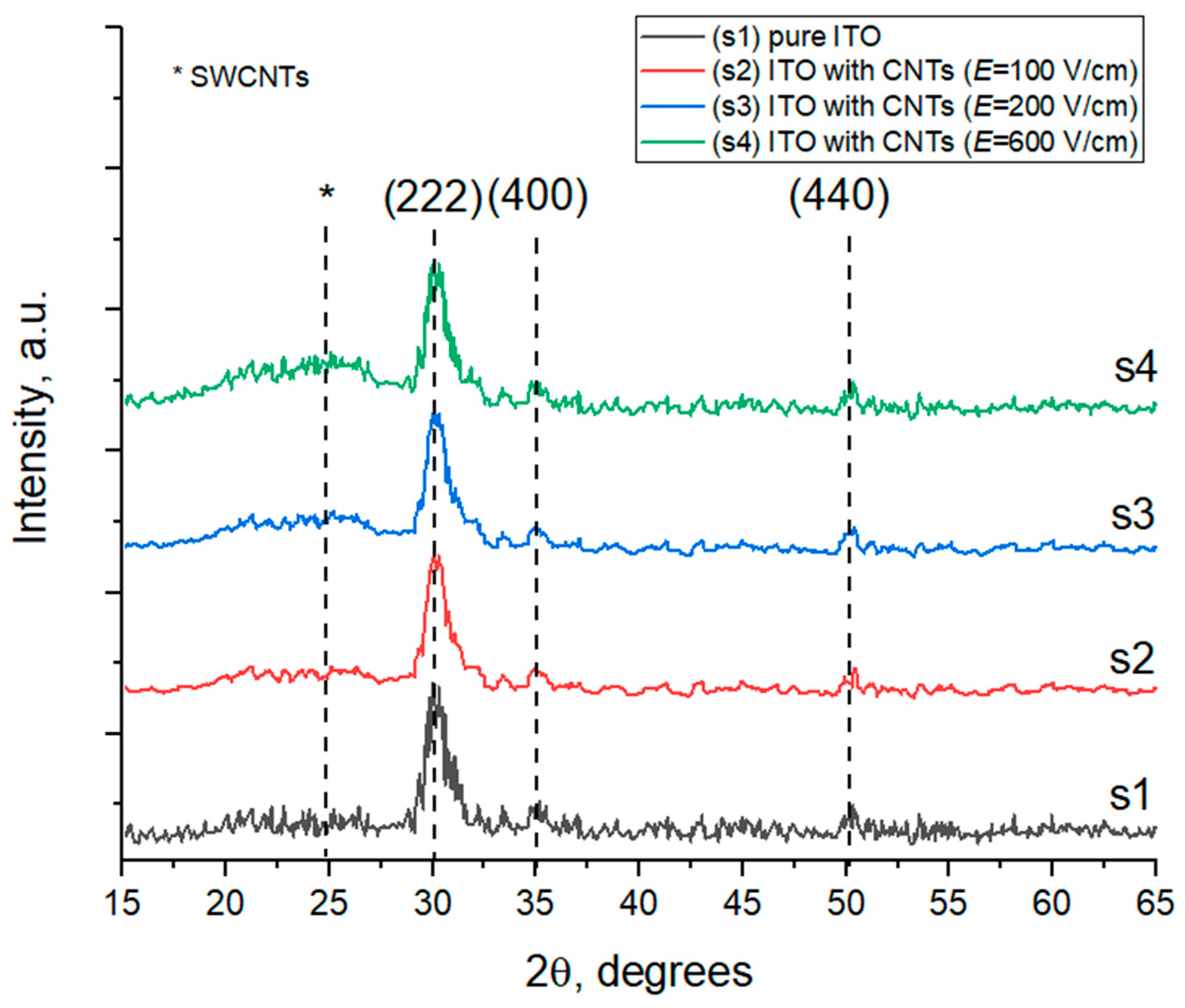
Analyzing the data from the XRD experiment (Table 4), one can postulate that in the case of acceleration in the control electric field (depends on E), the kinetic energy of CNTs rises during the LOD, so more particles have enough energy for the implantation into the ITO lattice.
(3)
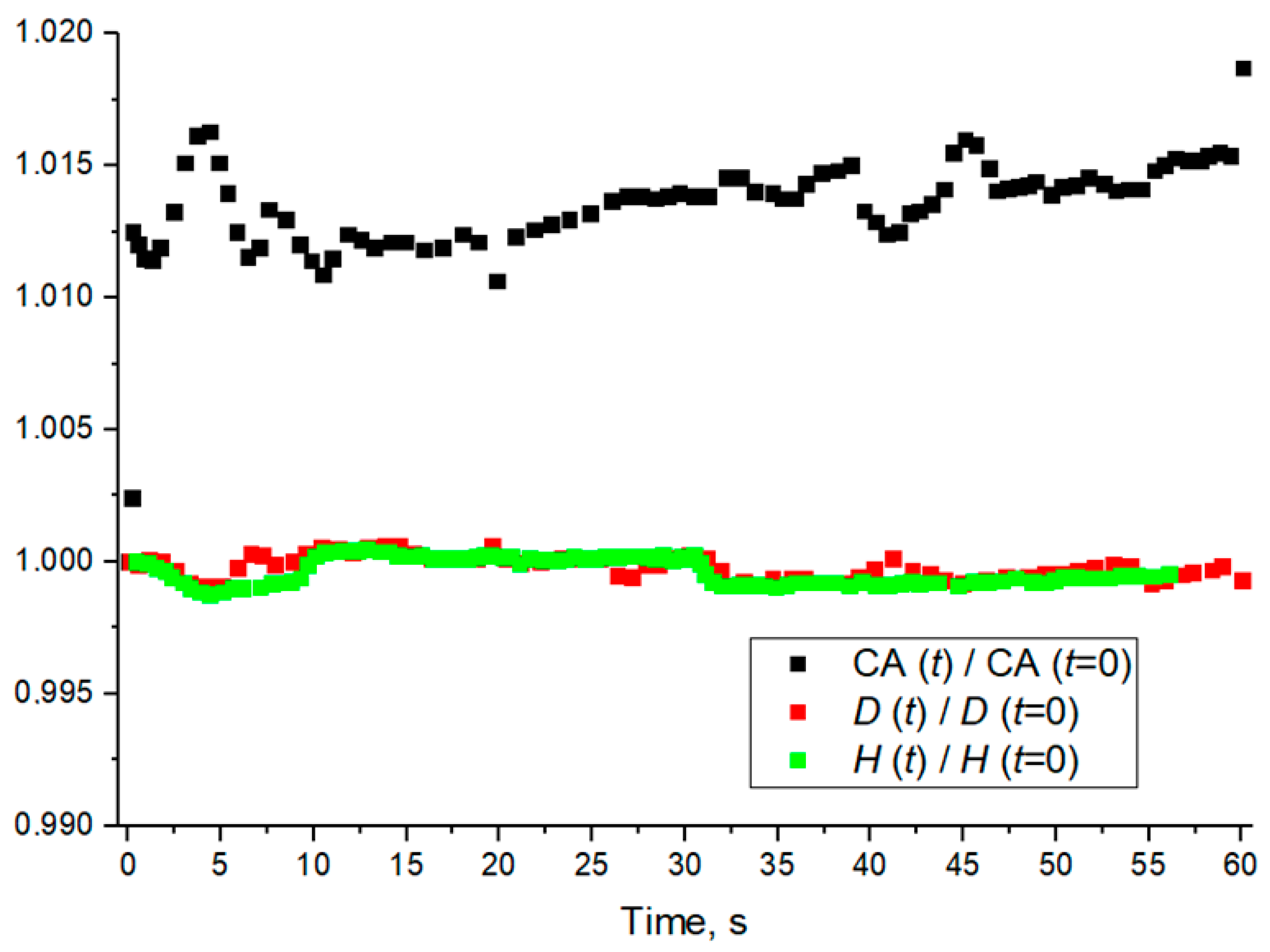
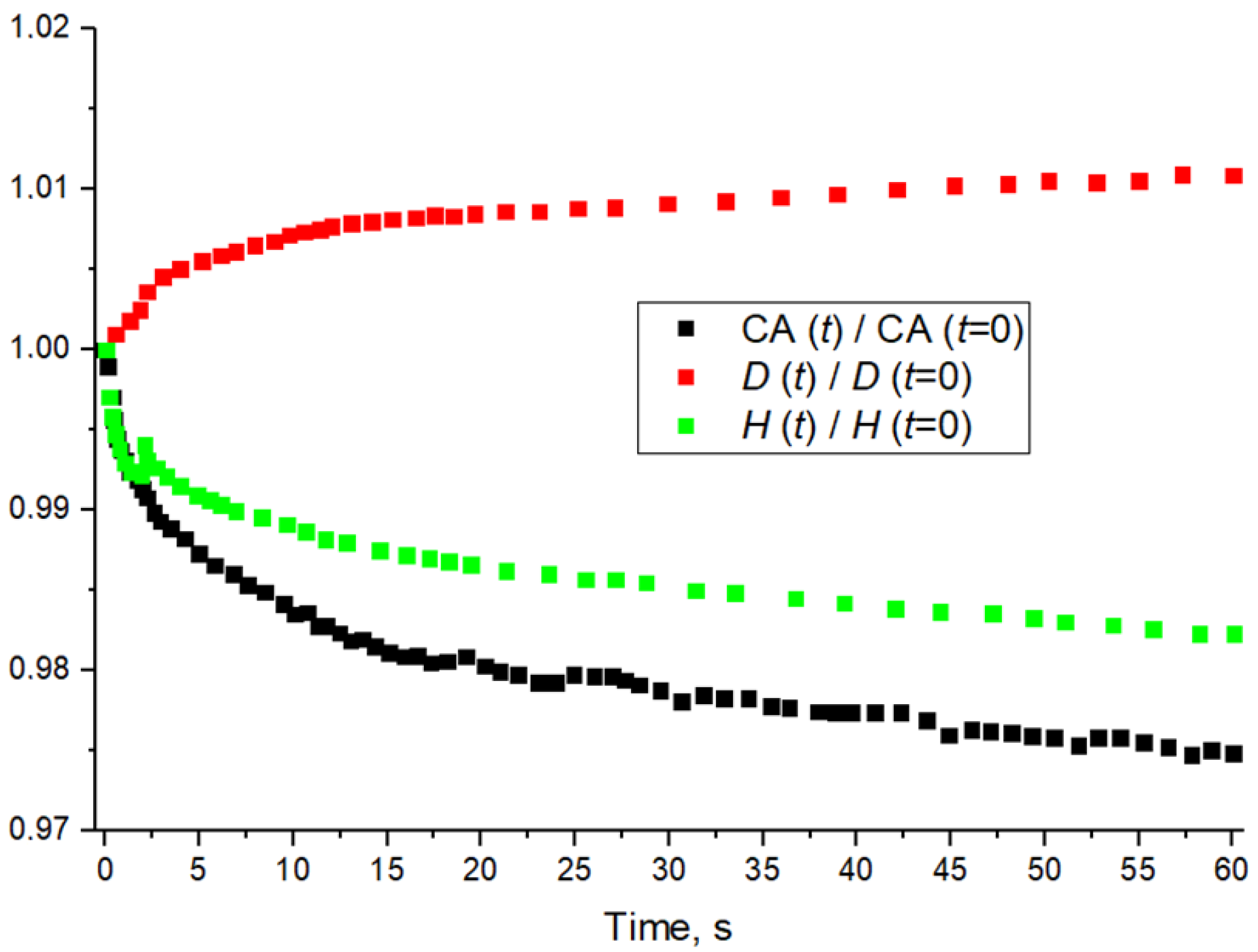
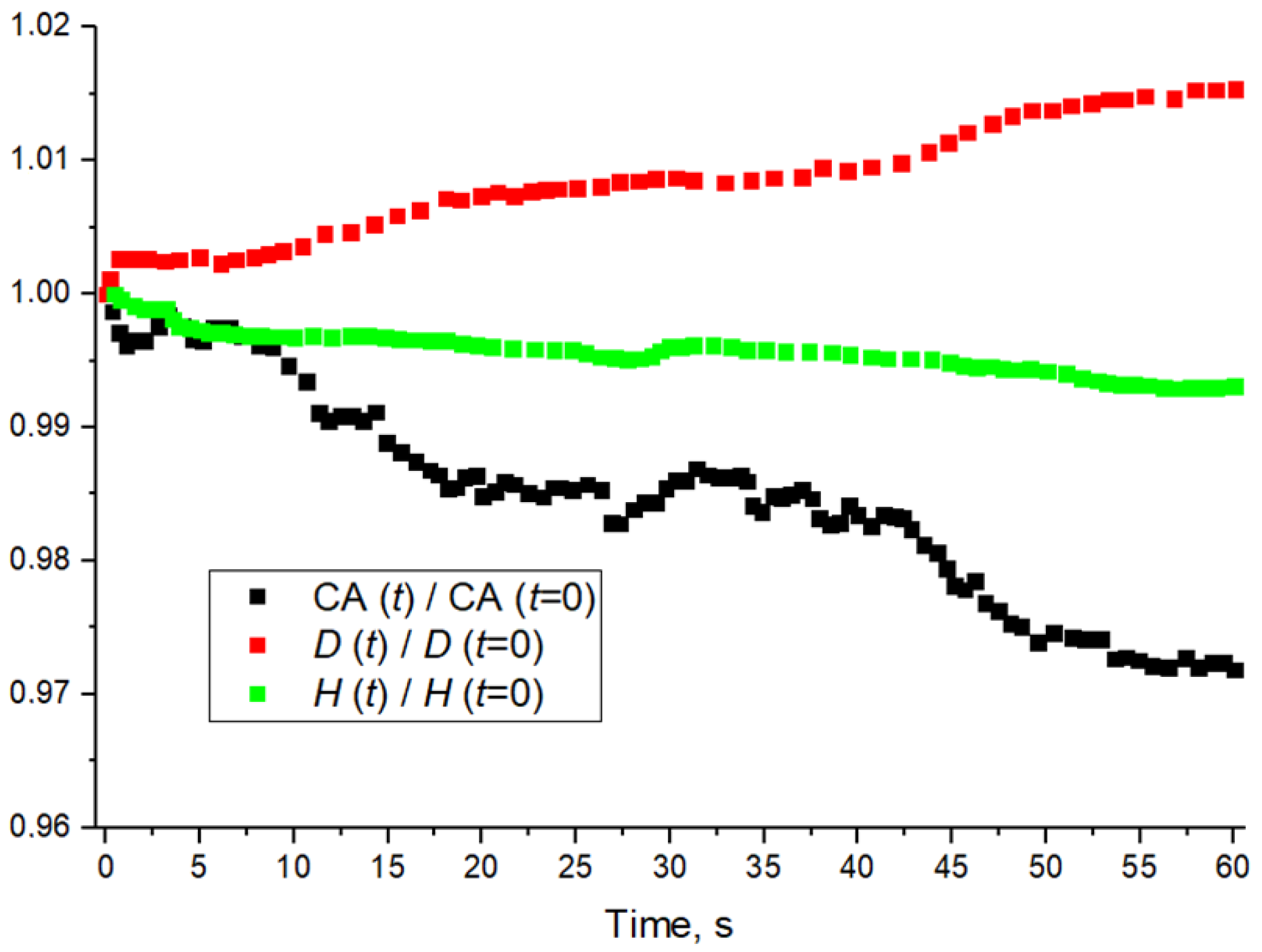
Via the dynamic wetting angle measurements of the “5CB- ITO” interfaces (Figure 3, Figure 4, Figure 5, Figure 6 and Figure 7), the principal difference mechanisms of the “viscous liquid—thin film” interactions were demonstrated. Due to this aspect, the ITO/CNT structures are potentially interesting technical decisions for microfluidics applications (as an alternative for ITO-based structures).
(4)
In terms of the liquid crystal (LC) technologies, the ITO/CNT structures allow the pre-tilt orientation to be switched (Table 4), which is useful for LC-based electro-optical modulators. Of course, given the fact that LC structures (LC display elements, LC convertor, LC modulator, etc.) function, as a rule, when they are placed between two polarizers, it is necessary to take into account the loss in transmission of the radiation passing through the LC layer.
(5)
All experiments and results obtained are well visualized. Consequently, many of these experiments can be recommended for the educational process in universities and schools.
In the next steps, it is reasonable to consider the influence of laser ablation and surface electromagnetic wave processing on the morphology of the ITO with CNTs—for issues related to the electro-optics, waterproof coatings, and the formation of microfluid channels. According to the liquid crystal device applications, consideration of the interfaces “ITO/CNTs—liquid crystals with the nanoparticles” is also required for the issues related to the mesophase orientation. Indeed, it would be interesting to consider the effect of the conducting ITO coatings structured with shungites or graphene oxides on the orientation ability of LC molecules.

Author Contributions

Conceptualization, resources, funding acquisition, formal analysis, review and editing, project administration, management of students and postgraduates, N.K.; methodology, software, validation, investigation, writing—original draft preparation, A.T.; investigation, M.I. All authors have read and agreed to the published version of the manuscript.

Funding

This research has been partially supported by the Russian Science Foundation, grant No. 24-23-00021.

Institutional Review Board Statement

Not applicable.

Informed Consent Statement

Not applicable.

Data Availability Statement

Publicly available data on laser-oriented CNTs deposition can be found in the patent: Kamanina, N.V.; Vasilyev, P.Y.; Studeonov, V.I. Optical Coating Based on Oriented in the Electric Field CNTs for the Optical Devises, Micro- and Nanoelectronics under the Conditions When the Interface: Solid Substrate-Coating Can Be Eliminated. RU Patent 2 405 177 C2, 23.12.2008.

Acknowledgments

The authors would like to thank their colleagues from the Lab for Photophysics at Vavilov State Optical Institute and colleagues from the Nuclear Physics Institute for the productive discussions at the seminars. The results of this work were partially presented in the International Conference “Applied Optics” (2022, St. Petersburg, Vavilov State Optical Institute), in the International Conference “SPbOPEN 2023” (2023, St. Petersburg, Higher School of Economics/Polytechnic University/Alferov University) and in the International Conference “Materials Science and Nanotechnology” (MSN-2023, Ural Federal University, Modern Nanotechnology Centre, Ekaterinburg, Russia, August 2023).

Conflicts of Interest

The authors have no conflict of interest.

References

  1. Zhang, K.; Zhu, F.; Huan, C.H.A.; Wee, A.T.S. Effect of hydrogen partial pressure on optoelectronic properties of indium tin oxide thin films deposited by radio frequency magnetron sputtering method. J. Appl. Phys. 1999, 86, 974–980. [Google Scholar] [CrossRef]
  2. Adurodija, F.O.; Izumi, H.; Ishihara, T.; Yoshioka, H.; Motoyama, M.; Murai, K. Influence of substrate temperature on the properties of indium oxide thin films. J. Vac. Sci. Technol. A 2000, 18, 814–818. [Google Scholar] [CrossRef]
  3. Kim, H.; Gilmore, C.M.; Pique, A.; Horwitz, J.S.; Mattoussi, H.; Murata, H.; Kafafi, Z.H.; Chrisey, D.B. Electrical, optical, and structural properties of indium–tin–oxide thin films for organic light-emitting devices. J. Appl. Phys. 1999, 86, 6451–6461. [Google Scholar] [CrossRef]
  4. Kerkache, L.; Layadi, A.; Mosser, A. Effect of oxygen partial pressure on the structural and optical properties of dc sputtered ITO thin films. J. Alloys Compd. 2009, 18, 46–50. [Google Scholar] [CrossRef]
  5. Socol, M.; Preda, N.; Rasoga, O.; Costas, A.; Stanculescu, A.; Breazu, C.; Gherendi, F.; Socol, G. Pulsed Laser Deposition of Indium Tin Oxide Thin Films on Nanopatterned Glass Substrates. Coatings 2019, 9, 19. [Google Scholar] [CrossRef]
  6. Ferhati, H.; Djeffal, F.; Benhaya, A. Optimized high-performance ITO/Ag/ITO multilayer transparent electrode deposited by RF magnetron sputtering. Superlattices Microstruct. 2019, 129, 176–184. [Google Scholar] [CrossRef]
  7. Fonollo-Rubio, R.; Placidi, M.; Hoelscher, T.; Thomere, A.; Li-Kao, Z.J.; Guc, M.; Izquierdo-Roca, V.; Scheer, R.; Perez-Rodriguez, A. Characterization of the Stability of Indium Tin Oxide and Functional Layers for Semitransparent Back-Contact Applications on Cu(in,Ga)Se2 Solar Cells. Solar RPL 2022, 6, 2101071. [Google Scholar] [CrossRef]
  8. Sahoo, A.K.; Kang, S.-Y.; Yu, P.; Pan, C.-L. Enhanced Optically–Excited THz Wave Emission by GaAs Coated with a Rough ITO Thin Film. Coatings 2023, 13, 461. [Google Scholar] [CrossRef]
  9. Sohmer, M.; Yudco, S.; Etgar, L. Mesoporous indium tin oxide perovskite solar cells in bifacial configuration. J. Phys. Energy 2022, 4, 045008. [Google Scholar] [CrossRef]
  10. Wan, C.; Qu, A.; Deng, L.; Liu, X.; Wu, C. Preparation of an electrochemical biosensor based on indium tin oxide and its performance in detecting antibiotic resistance genes. Microchem. J. 2022, 182, 107953. [Google Scholar] [CrossRef]
  11. Uludag, I.; Sezginturk, M.K. Ultrasensitive and Cost-Effective Detection of Neuropeptide-Y by a Disposable Immunosensor: A New Functionalization Route for Indium-Tin Oxide Surface. Biosensors 2022, 12, 925. [Google Scholar] [CrossRef] [PubMed]
  12. Tramarin, L.; Casquel, R.; Gil-Rostra, J.; Gonzalez-Martinez, M.A.; Herrero-Labrador, R.; Murillo, A.M.M.; Laguna, M.F.; Banuls, M.-J.; Gonzalez-Elipe, A.R.; Holgado, M. Design and Characterization of ITO-Covered Resonant Nanopillars for Dual Optical and Electrochemical Sensing. Chemosensors 2022, 10, 393. [Google Scholar] [CrossRef]
  13. Silah, H.; Erkmen, C.; Demir, E.; Uslu, B. Modified indium tin oxide electrodes: Electrochemical applications in pharmaceutical, biological, environmental and food analysis. Trends Anal. Chem. 2021, 141, 116289. [Google Scholar] [CrossRef]
  14. Lebedev, D.; Ezhov, R.; Heras-Domingo, J.; Comas-Vives, A.; Kaeffer, N.; Willinger, M.; Solans-Monfort, X.; Huang, X.; Pushkar, Y.; Coperet, C. Atomically Dispersed Iridium on Indium Tin Oxide Efficiently Catalyzes Water Oxidation. ACS Cent. Sci. 2022, 6, 1189–1198. [Google Scholar] [CrossRef]
  15. Chen, M.; Cao, X.; Chang, K.; Wang, R. A novel electrochemical non-enzymatic glucose sensor based on Au nanoparticle-modified indium tin oxide electrode and boronate affinity. Electrochim. Acta 2021, 368, 137603. [Google Scholar] [CrossRef]
  16. Kamanina, N.V.; Kukharchik, A.A.; Kuzhakov, P.V.; Zubtcova, Y.u.A.; Stepanov, R.O.; Baryshnikov, N.V. Modification of the conductive ITO layer by carbon nanotubes for orientation of liquid crystals in electro-optical optical information conversion devices. Liq. Cryst. Appl. 2015, 15, 109–118. [Google Scholar] [CrossRef]
  17. Kamanina, N.V.; Kukharchik, A.A.; Kuzhakov, P.V.; Zubtsova, Y.u.A.; Andraud, C.; Kajzar, F. Structural, optical and mechanical properties of nanostructured inorganic materials: Possible applications in biomedicine. Nonlinear Opt. Quantum Opt. 2015, 47, 131–138. [Google Scholar]
  18. Kamanina, N.V.; Likhomanova, S.V.; Zubtsova, Y.u.A.; Kuzhakov, P.V.; Zimnukhov, M.A.; Vasil’ev, P.Y.; Studenov, V.I. Surface modification of materials using laser-oriented nanostructuring. J. Opt. Technol. 2018, 85, 722–728. [Google Scholar] [CrossRef]
  19. Sousa, M.G.; da Cuncha, A.F. Optimization of low temperature RF-magnetron sputtering of indium tin oxide films for solar cell applications. Appl. Surf. Sci. 2019, 484, 257–264. [Google Scholar] [CrossRef]
  20. Bhorde, A.; Waykar, R.; Nair, S.; Borate, H.; Pandharkar, S.; Aher, R.; Waghmare, A.; Vairale, P.; Naik, D.; Jadkar, S. Room Temperature Synthesis of Transparent and Conducting Indium Tin Oxide Films with High Mobility and Figure of Merit by RF-Magnetron Sputtering. J. Electron. Mater. 2019, 48, 7192–7202. [Google Scholar] [CrossRef]
  21. Yang, S.; Sun, B.; Liu, Y.; Zhu, J.; Song, J.; Hao, Z.; Zeng, X.; Zhao, X.; Shu, Y.; Chen, J.; et al. Effect of ITO target crystallinity on the properties of sputtering deposited ITO films. Ceram. Int. 2020, 46, 6342–6350. [Google Scholar] [CrossRef]
  22. Singh, G.; Sheokand, H.; Ghosh, S.; Srivastava, K.V.; Ramkumar, J.; Ramakrishna, S.A. Excimer laser micromachining of indium tin oxide for fabrication of optically transparent metamaterial absorbers. Appl. Phys. A 2019, 125, 23. [Google Scholar] [CrossRef]
  23. Kamanina, N.; Toikka, A.; Gladysheva, I. ITO conducting coatings properties improvement via nanotechnology approach. Nano Express 2021, 2, 010006. [Google Scholar] [CrossRef]
  24. Kamanina, N.V.; Vasilyev, P.Y.; Studeonov, V.I. Optical Coating Based on Oriented in the Electric Field CNTs for the Optical Devises, Micro- and Nano-Electronics under the Conditions When the Interface: Solid Substrate-Coating Can Be Eliminated. RU Patent 2,405,177 C2, 23 December 2008. [Google Scholar]
  25. Ozkartal, A. Characterization of the ITO/p-Si/Al contacts produced by thermal evaporation. Vacuum 2019, 168, 108799. [Google Scholar] [CrossRef]
  26. Jain, P.; Singh, S.; Pundir, S.K. Synthesis of Highly Transparent Indium Tin Oxide Thin Films Using Vacuum Evaporation Technique. J. Nanosci. Nanotechnol. 2020, 20, 3845–3853. [Google Scholar] [CrossRef]
  27. Hosen, M.M.; Atique Ullah, A.K.M.; Haque, M.M.; Abdur Rahim, S.M.; Abdus Sobahan, K.M.; Khan, M.N.I. Optical and electrical properties of crystalline indium tin oxide thin film deposited by vacuum evaporation technique. Optoelectron. Lett. 2019, 15, 356–359. [Google Scholar] [CrossRef]
  28. Kim, H.; Horwitz, J.S.; Kushto, G.; Pique, A.; Kafafi, Z.H.; Gilmore, C.M.; Chrisey, D.B. Effect of film thickness on the properties of indium tin oxide thin films. J. Appl. Phys. 2000, 88, 6021–6025. [Google Scholar] [CrossRef]
  29. Sun, K.; Yang, C.; Zhang, D.; Jin, D.; Wei, Y.; Yuan, H. Effects of ambient high-temperature annealing on microstructure, elemental composition, optical and electrical properties of indium tin oxide films. Mater. Sci. Eng. B 2022, 276, 115534. [Google Scholar] [CrossRef]
  30. Besbes, S.; Ben Ouada, H.; Davenas, J.; Ponsonnet, L.; Jaffrezic, N.; Alcouffe, P. Effect of surface treatment and functionalization on the ITO properties for OLEDs. Mater. Sci. Eng. C 2006, 26, 505–510. [Google Scholar] [CrossRef]
  31. Rong, X.; Han, J.; Tian, X.; Li, L.J.Z.; Xing, R.; Shen, L.; Duan, L.; Dong, G. Modification of Indium Tin Oxide Surface with HCl for Source/Drain Electrodes in Organic Thin Film Transistors. Adv. Mater. Technol. 2022, 7, 2101487. [Google Scholar] [CrossRef]
  32. El Nahrawy, A.M.; Abou Hammad, A.B.; Youssef, A.M.; Mansour, A.M.; Othman, A.M. Thermal, dielectric and antimicrobial properties of polystyrene-assisted/ITO: Cu nanocomposites. Appl. Phys. A 2019, 125, 46. [Google Scholar] [CrossRef]
  33. Mei, F.; Huang, J.; Yuan, T.; Li, R. Effect of cerium doping on the microstructure and photoelectric properties of Ce-doped ITO films. Appl. Surf. Sci. 2020, 509, 144810. [Google Scholar] [CrossRef]
  34. Gartner, M.; Anastasescu, M.; Calderon-Moreno, J.M.; Nicolescu, M.; Stroescu, H.; Hornoiu, C.; Preda, S.; Predoana, L.; Mitrea, D.; Covei, M.; et al. Multifunctional Zn-Doped ITO Sol–Gel Films Deposited on Different Substrates: Application as CO2-Sensing Material. Nanomaterials 2022, 12, 3244. [Google Scholar] [CrossRef]
  35. Umeyama, T.; Imahori, H. Isomer Effects of Fullerene Derivatives on Organic Photovoltaics and Perovskite Solar Cells. Acc. Chem. Res. 2019, 52, 2046–2055. [Google Scholar] [CrossRef]
  36. Lin, H.-S.; Jeon, I.; Chen, Y.; Yang, X.-Y.; Nakagawa, T.; Maruyama, S.; Manzhos, S.; Matsuo, Y. Highly Selective and Scalable Fullerene-Cation-Mediated Synthesis Accessing Cyclo[60]fullerenes with Five-Membered Carbon Ring and Their Application to Perovskite Solar Cells. Chem. Mater. 2019, 31, 8432–8439. [Google Scholar] [CrossRef]
  37. Brabec, C.J.; Padinger, F.; Sariciftci, N.S.; Hummelen, J.C. Photovoltaic properties of conjugated polymer/methanofullerene composites embedded in a polystyrene matrix. J. Appl. Phys. 1999, 85, 6866–6972. [Google Scholar] [CrossRef]
  38. Golobostanfard, M.R.; Mohammadi, S.; Abdizadeh, H.; Baghchesara, M.A. Incorporating Carbon Nanotubes in Sol–Gel Synthesized Indium Tin Oxide Transparent Conductive Films. Langmuir 2014, 30, 11785–11791. [Google Scholar] [CrossRef]
  39. Koo, J.; Lee, S.; Cho, S. Effect of Additives on the Properties of Printed ITO Sensors. J. Korean Phys. Soc. 2017, 71, 335–339. [Google Scholar] [CrossRef]
  40. Kamanina, N.; Toikka, A.; Kvashnin, D. Nanostructuration Impact on the Basic Properties of the Materials: Novel Composite Carbon Nanotubes on a Copper Surface. J. Compos. Sci. 2022, 6, 181. [Google Scholar] [CrossRef]
  41. Kamanina, N.; Toikka, A.; Barnash, Y.; Kuzhakov, P.; Kvashnin, D. Advanced and Functional Structured Ceramics: MgF2 and ZnS. Materials. 2022, 15, 4780. [Google Scholar] [CrossRef]
  42. Kamanina, N.; Toikka, A.; Valeev, B.; Kvashnin, D. Carbon Nanotubes Use for the Semiconductors ZnSe and ZnS Material Surface Modification via the Laser-Oriented Deposition Technique. C 2021, 7, 84. [Google Scholar] [CrossRef]
  43. Kamanina, N.V.; Vasil’ev, P.Y.; Studeonov, V.I.; Usanov Yu, E. Strengthening transparent conductive coatings and “soft” materials of the IR range when nanotechnologies are used. J. Opt. Technol. 2008, 75, 67–68. [Google Scholar] [CrossRef]
  44. Kamanina, N. Carbon Nanotube Coatings Role in Transparency, Mechanical Hardness, and Wetting Angle Increase. Coatings 2022, 12, 1279. [Google Scholar] [CrossRef]
  45. Tsai, H.-Y.; Hsu, C.-N.; Li, C.-R.; Lin, Y.-H.; Hsiao, W.-T.; Huang, K.-C.; Yen, J.A. Surface Wettability and Electrical Resistance Analysis of Droplets on Indium-Tin-Oxide Glass Fabricated Using an Ultraviolet Laser System. Micromachines 2021, 12, 44. [Google Scholar] [CrossRef]
  46. Song, Z.-R.; Zeng, J.; Zhou, J.-L.; Yan, B.-Y.; Gu, Z.; Wang, H.-F. Optimization of Electrode Patterns for an ITO-Based Digital Microfluidic through the Finite Element Simulation. Micromachines 2022, 13, 1563. [Google Scholar] [CrossRef]
  47. Nsabimana, J.; Wang, Y.; Ruan, Q.; Li, T.; Shen, H.; Yang, C.; Zhu, Z. An electrochemical method for a rapid and sensitive immunoassay on digital microfluidics with integrated indium tin oxide electrodes coated on a PET film. Analyst 2021, 146, 4473–4479. [Google Scholar] [CrossRef]
  48. Owens, D.K.; Wendt, R.C. Estimation of the surface free energy of polymers. J. Apply. Polym. Sci. 1969, 13, 1741–1747. [Google Scholar] [CrossRef]
  49. Toosi, S.F.; Moradi, S.; Hatzikiriakos, S.G. Fabrication of Micro/Nano Patterns on Polymeric Substrates Using Laser Ablation Methods to Control Wettability Behaviour: A Critical Review (Chapter 2). Prog. Adhes. Adhes. 2018, 3, 53–75. [Google Scholar] [CrossRef]
  50. Good, R.J. Contact angle, wetting, and adhesion: A critical review. J. Adhes. Sci. Technol. 1992, 6, 1269–1302. [Google Scholar] [CrossRef]
  51. Rebinder, P.A. Superfical Phenomena in Dispersed Systems; Colloid Chemistry; Nauka: Moscow, Russia, 1978; pp. 300–332. (In Russian) [Google Scholar]
  52. Summ, B.D.; Goryunov, Y.V. Phys-Chemical Foundations of Wetting and Spreading; Himiya: Moscow, Russia, 1976; 232p. (In Russian) [Google Scholar]
  53. Kamanina, N.V.; Toikka, A.S.; Barnash, Y.a.V.; Redka, D.N.; Lihkomanova, S.V.; Zybtsova, Y.u.A.; Kyzhakov, P.V.; Jovanovic, Z.; Jovanovic, S. Functioning features of liquid crystalline cells doped with CoFe2O4 nanoparticles. Liq. Cryst. Their Appl. 2022, 22, 83–91. [Google Scholar] [CrossRef]
  54. Kamanina, N.V.; Zubtsova, Y.A.; Toikka, A.S.; Likhomanova, S.V.; Zak, A.; Tenne, R. Temporal Characteristics of Liquid Crystal Cell with WS2 Nanoparticles: Mesophase Sensitization and Relief features. Liq. Cryst. Their Appl. 2020, 20, 34–40. [Google Scholar] [CrossRef]
  55. Sofi, A.H.; Shah, M.A.; Asokan, K. Structural, Optical and Electrical Properties of ITO thin films. J. Electron. Mater. 2018, 47, 1344–1352. [Google Scholar] [CrossRef]
  56. Kerkache, L.; Layadi, A.; Dogheche, E.; Remiens, D. Physical properties of RF sputtered ITO thin films and annealing effect. J. Phys. D Appl. Phys. 2006, 39, 184–189. [Google Scholar] [CrossRef]
  57. Kim, J.H.; Jeon, K.A.; Kim, G.H.; Lee, S.Y. Electrical, structural, and optical properties of ITO thin films prepared at room temperature by pulsed laser deposition. Appl. Surf. Sci. 2006, 252, 4834–4837. [Google Scholar] [CrossRef]
  58. Merck. Sigma-Aldrich: Carbon Nanotube Single-Walled, 704121. Available online: https://www.sigmaaldrich.com/RU/en/product/aldrich/704121 (accessed on 15 December 2023).
  59. Mitsuyama, R.; Tadera, S.; Kyakuno, H.; Suzuki, R.; Ishii, H.; Nakai, Y.; Miyata, Y.; Yanagi, K.; Kataura, H.; Maniwa, Y. Chirality fingerprinting and geometrical determination of single-walled carbon nanotubes: Analysis of fine structure of X-ray diffraction pattern. Carbon 2014, 75, 299–306. [Google Scholar] [CrossRef]
  60. Miyata, Y.; Yanagi, K.; Maniwa, Y.; Tanaka, T.; Kataura, H. Diameter Analysis of Rebundled Single-Wall Carbon Nanotubes Using X-ray Diffraction: Verification of Chirality Assignment Based on Optical Spectra. J. Phys. Chem. C 2008, 112, 15997–16001. [Google Scholar] [CrossRef]
  61. Futaba, D.N.; Yamada, T.; Kobashi, K.; Yumura, M.; Hata, K. Macroscopic wall number analysis of single-walled, double-walled and few-walled carbon nanotubes by X-ray diffraction. J. Am. Chem. Soc. 2011, 133, 5716–5719. [Google Scholar] [CrossRef]
  62. Ferreira, S.H.; Morais, M.; Nunes, D.; Oliveira, M.J.; Rovisco, A.; Pimentel, A.; Águas, H.; Fortunato, E.; Martins, R. High UV and Sunlight Photocatalytic Performance of Porous ZnO Nanostructures Synthesized by a Facile and Fast Microwave Hydrothermal Method. Materials 2021, 14, 2385. [Google Scholar] [CrossRef] [PubMed]
  63. Muslimov, A.E.; Asvarov, A.S.; Shabanov, N.C.; Kanevsky, V.M. The influence of topographic defects on the superhydrophobic properties of coatings based on ZnO. Tech. Phys. Lett. 2020, 46, 15–18. (In Russian) [Google Scholar] [CrossRef]
  64. Jain, N.; Sharma, S.; Puri, N.K. Investigation of charge transport mechanism in hydrothermally synthesized reduced graphene oxide (rGO) incorporated zinc oxide (ZnO) nanocomposite films. J. Mater. Sci. Mater. Electron. 2022, 33, 1307–1323. [Google Scholar] [CrossRef]
  65. Bukhari, S.N.U.S.; Shah, A.A.; Bhatti, M.A.; Tahira, A.; Channa, I.A.; Shah, A.K.; Chandio, A.D.; Mahdi, W.A.; Alshehri, S.; Ibhupoto, Z.H.; et al. Psyllium-Husk-Assisted Synthesis of ZnO Microstructures with Improved Photocatalytic Properties for the Degradation of Methylene Blue (MB). Nanomaterials 2022, 12, 3568. [Google Scholar] [CrossRef] [PubMed]
  66. Nosidlak, N.; Jaglarz, J.; Vallati, A.; Dulian, P.; Jurzecka-Szymacha, M.; Gierałtowska, S.; Seweryn, A.; Wachnicki, Ł.; Witkowski, B.S.; Godlewski, M. The Optical Properties of Thin Film Alloys of ZnO, TiO2 and ZrO2 with Al2O3 Synthesised Using Atomic Layer Deposition. Coatings 2023, 13, 1872. [Google Scholar] [CrossRef]
Figure 1. SEM images of the ITO modifications: (a) pure ITO; (b) ITO with CNTs (E = 200 V/cm).
Coatings 14 00178 g001
Figure 2. Atomic force profile of the ITO modifications: (a) pure ITO; (b) ITO with CNTs (E = 100 V/cm); (c) ITO with CNTs (E = 200 V/cm); (d) ITO with CNTs (E = 600 V/cm).
Coatings 14 00178 g002
Figure 3. The wetting angle hysteresis of ITO modification for the distilled water drops.
Coatings 14 00178 g003
Figure 4. XRD data of the laser-oriented modifications of ITO thin films: s1—pure ITO; s2—ITO with CNTs (E = 100 V/cm); s3—ITO with CNTs (E = 200 V/cm); s4—ITO with CNTs (E = 600 V/cm).
Coatings 14 00178 g004
Figure 5. The temporal dynamic of the contact angle (CA), drop diameter (D) and height (H) for the system “5CB-pure ITO”.
Coatings 14 00178 g005
Figure 6. The temporal dynamic of the contact angle (CA), drop diameter (D) and height (H) for the “5CB-ITO with CNTs (E = 100 V/cm)” system.
Coatings 14 00178 g006
Figure 7. The possible mechanism of the height and volume of the 5CB drop on the ITO with the CNT surface changing: (a) the moment of the contact of the drop with the surface (left) and the absorption of the drop by the surface with the formation of air bubbles (right); (b) droplet evaporation, air–droplet interface before the air bubbles crossing (left) and after (right).
Coatings 14 00178 g007
Figure 8. The temporal dynamic of the contact angle (CA), drop diameter (D) and height (H) for the “5CB-ITO with CNTs (E = 200 V/cm)” system.
Coatings 14 00178 g008
Figure 9. The temporal dynamic of the contact angle (CA), drop diameter (D) and height (H) for the “5CB-ITO with CNTs (E = 600 V/cm)” system.
Coatings 14 00178 g009
Table 1. Values of free tension components for used liquids in the wetting angle measurements.
Liquidγlp, mN/mγld, mN/mγl, mN/m
Water48.124.172.2
Toluene1.327.228.5
Table 2. Calculated root mean square roughness of the ITO modifications from the AFM data.
SampleII Order FittingIII Order Fitting
AverageStandard DeviationAverageStandard Deviation
Pure ITO11.64.74.41.7
ITO with CNTs
(E = 100 V/cm)
13.42.67.66.4
ITO with CNTs
(E = 200 V/cm)
51.19.825.45.4
ITO with CNTs
(E = 600 V/cm)
86.513.117.84.4
Table 3. Comparison of Young’s angles and SFE components of the ITO modifications.
SampleYoung’s Angle, °Surface Free Energy, mJ/m2
WaterToluenePolarDispersive
Pure ITO85.3517.38.222.2
ITO with CNTs
(E = 100 V/cm)
115.6524.90.829.2
ITO with CNTs
(E = 200 V/cm)
95.6522.71.325.0
ITO with CNTs
(E = 600 V/cm)
119.519.11.831.4
Table 4. XRD peaks of the ITO thin films.
LabelStructure(222)(400)(440)
2θ, Deg.FWHM, Deg.2θ, Deg.FWHM, Deg.2θ, Deg.FWHM, Deg.
s1Pure ITO30.1881.14135.0530.77750.3071.027
s2ITO + CNTs (E = 100 V/cm)30.1831.12135.0350.87450.3041.184
s3ITO + CNTs (E = 200 V/cm)30.1811.13335.0020.70250.2921.128
s4ITO + CNTs (E = 600 V/cm)30.1651.37335.0661.26850.2391.140
Table 5. Contact angles of 5CB drop at various times on surfaces of ITO modifications.
SampleMoment of Contact (t = 0 s)Saturation
Condition
1 min Later
(t = 60 s)
Pure ITO39.538.35 (t = 2.9 s)38.25
ITO with CNTs
(E = 100 V/cm)
52.152.8 (t = 4.8 s) 153.15
ITO with CNTs
(E = 200 V/cm)
60.158.95 (t = 2.7 s)58.6
ITO with CNTs
(E = 600 V/cm)
58.558.4 (t = 1.6 s)56.85
1 Contact angle has no saturation; for these conditions, the transition “absorption–spreading” was observed.
Disclaimer/Publisher’s Note: The statements, opinions and data contained in all publications are solely those of the individual author(s) and contributor(s) and not of MDPI and/or the editor(s). MDPI and/or the editor(s) disclaim responsibility for any injury to people or property resulting from any ideas, methods, instructions or products referred to in the content.

