Abstract
The disintegration of a continuous metallic thin film leads to the formation of isolated islands, which can be used for the preparation of plasmonic structures. The transformation mechanism is driven by a thermally accelerated diffusion that leads to the minimalization of surface free energy in the system. In this paper, we report the results of our study on the disintegration of gold thin film and the formation of nanoislands on silicon substrates, both pure and with native silicon dioxide film. To study the processes leading to the formation of gold nanostructures and to investigate the effect of the oxide layer on silicon diffusion, metallic film with a thickness of 3 nm was deposited by molecular beam epitaxy (MBE) technique on both pure and oxidized silicon substrates. Transformation of the thin film was observed by low-energy electron microscopy (LEEM) and a scanning electron microscope (SEM), while the nanostructures formed were observed by atomic force microscope (AFM) method. Structural investigations were performed by low-energy electron diffraction (LEED) and X-ray photoelectron spectroscopy (XPS) methods. Our experiments confirmed a strong correlation between the formation of nanoislands and the presence of native oxide on silicon substrates.
1. Introduction
Continuous solid metallic nanometric thin films can be meta- or unstable after deposition. This results in disintegration (dewetting) of the continuous layer into isolated nanoislands [1,2,3,4]. That process can be observed at temperatures well below the melting point of the nanolayer material, even at room temperature. The transformation mechanism is driven by a thermally accelerated diffusion that leads to the minimalization of surface free energy in the system [5,6,7,8]. Thin films, especially those with nanometer-scale thicknesses, have a relatively high surface energy and a large interfacial area with the substrate. This can create a driving force for the film to undergo dewetting and finally to form isolated islands. This process is governed by the balance between the energy required to create new surfaces (surface tension) and the energy gained by reducing the total interfacial area (interfacial tension) [9,10,11,12]. However, even if the thermodynamics of the system are known, there is no clear step-by-step explanation of the microscopic mechanism and kinetics of the dewetting process. Drawing from our previous experiments with gold, silver, and bimetallic Au-Ag alloyed nanostructures, we can explain the growth of metallic islands from thin films as the nucleation of holes on the film’s surface [13,14,15]. These holes appear at the grain borders, preferably at the triple junctions, so-called T-junctions, of boundaries [16,17,18,19]. Additionally, the nucleation of holes can be accelerated by surface melting or premelting, especially in a region with a lower film thickness at grain boundaries [20,21,22]. Then, a thin layer of liquid phase can cover solid grains, which accelerates disintegration of the thin film. The holes expand and the material diffuses, creating both raised ridges and grooves in the places of grain boundaries. These structures transform into isolated islands. Finally, as a result of melting, isolated and irregularly shaped islands evolve into spherical droplets. Melting occurs at temperatures well below the melting point of the bulk material, which is in line with theory [13,23,24]. It should be noted that the process can become more complicated when a eutectic forms between the thin film and the substrate. It could play a key role, especially in nanoscale systems, when both the eutectic temperature drastically decreases and the eutectic composition changes, with size reduction [25,26,27,28]. Disintegration of the metallic films could be a problem; for example, during electrical measurements in a wide range of temperatures, which was described by Wójcik et al. [29]. On the other hand, dewetting may lead to the formation of plasmonic nanostructures, so-called plasmonic platforms, which has been described in more detail in our previous publications [13,14,23,30,31,32,33].
In this work, we report the results of our study on the disintegration of gold thin film and the formation of nanoislands. To study the effect of silicon diffusion on processes of dewetting and the formation of gold nanostructures, thin metallic Au films were deposited on silicon substrates with and without the native oxide film. The disintegration process was measured in two ways: by analyzing SEM images of annealed samples, as well as during in situ measurements by LEEM and LEED.
2. Materials and Methods
The gold films were deposited by molecular beam epitaxy (MBE) method. For the future SEM measurements, two 2 inch Si wafers were first heated under a vacuum of 2 × 10⁻⁷ mbar in the load-lock chamber of the MBE system for 3 h at 150 °C to remove adsorbed gases. Next, one of them was annealed under UHV in the growth chamber at ~1000 °C to remove the native oxide film, as monitored by reflection high-energy electron diffraction (RHEED) technique (k-Space Associates, Inc., Dexter, MI, USA). When cooling the wafer to ~830 °C, the RHEED pattern changed from 1 × 1 to 7 × 7, which clearly indicated a clean surface of Si(111) substrate. Then, deposition of nominally 2.8 nm thick Au film was performed on both substrates at room temperature with the rate of 0.6 nm/min. A resistively heated source of Au was used and pressure in the growth chamber during Au deposition was below 3 × 10⁻⁹ mbar. Moreover, evaporated thin films were annealed in a furnace for selected time and temperatures. The results of thermal treatment were observed by the FEI Quanta FEG 250 Scanning Electron Microscope (SEM) (FEI, Hillsboro, OR, USA) operating at 10 kV. For the in situ LEEM and LEED observations, a second series of gold films was prepared and deposited on two types of substrates: precleaned (111) silicon and silicon covered by native oxide. The Si(111) substrates had been flashed under UHV to obtain the clean surface characterized by the (7 × 7) reconstruction. The cleaning procedure was described in our previous work [34]. Silicon wafers with native oxide had been heated at 140 °C in order to remove absorbed water. The MBE deposition process was conducted at room temperature and a pressure below 3 × 10⁻¹⁰ mbar. Sixteen monolayers of Au were deposited from the resistively heated crucible with a rate of 0.2 mL/min. The evaporation rate had been determined during previous experiments [35] and additionally confirmed by the atomic force microscope (AFM) measurement on a step created by masking the thin film. The thickness and topography of the samples was investigated by Atomic Force Microscope NT-MDT Ntegra (NT-MDT, Moscow, Russia) in a contact mode. In situ observations of the thermal disintegration of the thin films were performed by the Elmitec Low-Energy Electron Microscope (LEEM) and the low-energy electron diffraction (LEED) (Elmitec, Clausthal-Zellerfeld, Germany) method during sample annealing under vacuum conditions. Additionally, X-ray photoemission spectroscopy (XPS) (ScientaOmicron, Uppsala, Sweden) and the energy-dispersive X-ray spectrometer (EDS) (Ametek, Berwin, PA, USA) for elemental analysis of nanoislands were used.
3. Results
The thickness of gold films evaporated on silicon substrate was determined by AFM method. The profile was measured on a step created by masking the film during evaporation. A typical profile line scan is presented in Figure 1. Measurements showed that an average thickness of 16 mL film is equal to ca. 3 nm. It should be noted that the thickness value is obtained by averaging several height profiles to eliminate random errors. Furthermore, it should be noted that we evaporated nominally 16 mL and the layer thickness is calculated by taking 1 mL Au as the distance between the (111) Au planes. This applies to the situation where Au is deposited on pure Si. On the other hand, in the case of an amorphous substrate the same amount of Au is evaporated, as on pure Si, but the Au grows in amorphous form. It is difficult to determine its thickness in relation to monolayers. It is also impossible to determine what orientation the layers are in during growth.
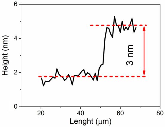
Figure 1.
Thickness profile of 16 ML of Au evaporated on Si substrate.
The disintegration of the Au films was observed by LEEM. Measurements were performed in situ during heating under vacuum conditions. It was noticed that during heating grain boundaries appeared on a continuous film. When the temperature ramped from RT up to ca. 415 K the first voids were observed. Figure 2 shows an LEEM image of a hole at a multiple junction between grains. This could be considered as the beginning of the growth of voids and the starting point of the disintegration of the thin film. Our microscopic observation is perfectly in line with the literature data [16,17,18,19]. Further disintegration of the gold film is shown in the sequence of LEEM images presented in Figure 3. As seen, upon heating the voids grew and initially irregular-shaped gold structures were formed. Similar results were obtained by Święch et al., during observations of the disintegration of submonolayer gold film on silicon [36]. The process of the formation of isolated gold or silver islands was described in detail in our previous work, e.g., in [13,14].
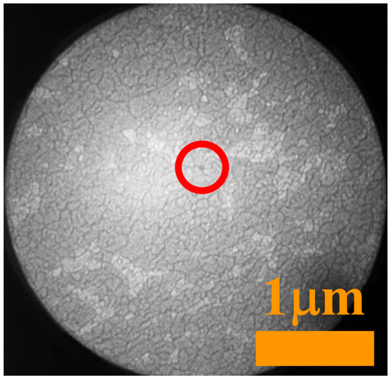
Figure 2.
LEEM image of the 16 mL Au film evaporated on Si, annealed at 415 K. A void at a multiple junction between grains is marked by the circle.
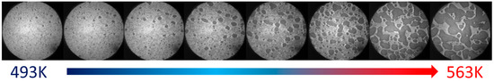
Figure 3.
In situ LEEM images of the 16 mL Au film evaporated on a pure Si substrate, annealed at various temperatures. The diameter of the circular field is 5 μm.
The growth process and temperature-induced disintegration of the 16 ML thick Au layer deposited on both clean Si and native silicon oxide substrates were followed by low-energy electron diffraction (LEED). The large blurry spot observed in Figure 4a–d in the vicinity of the (0, 0) spot is associated with inelastic back-scattered electrons and can be considered as a background. Figure 4a shows a typical diffraction pattern of the Si(111)-(7 × 7) reconstructed surface that we observe for an atomically clean and well-ordered surface of Si(111). In contrast to the clean Si surface, the native silicon oxide reveals an amorphous character, which is manifested by the absence of diffraction spots (not shown). Figure 4b shows the diffraction pattern collected after deposition of the Au layer with a thickness of 16 mL on the clean Si substrate. During the deposition of the Au layer, a significant diffusion of Si atoms from the substrate across the Au layer is observed. The diffused Si atoms segregate on the surface of the Au layer, forming a weak-ordered low-buckled phase of silicene at room temperature, which is observed as a blurry ring of diffraction spots. In this case, heating the sample to a temperature close to the temperature of decomposition of the Au layer leads to the formation of a well-ordered planar phase of silicene on the top of the Au layer [37,38]. The formation of silicene in such a system is beyond the scope of this manuscript and a detailed description of such a process has been already published elsewhere [35]. The Au layer deposited on the amorphous native silicon oxide also has an amorphous character and again no diffraction spots are observed (not shown). Figure 4c,d show diffraction patterns collected after temperature-induced disintegration of the Au layer deposited on clean Si and native Si oxide, respectively. In the first case (4c), the hexagonal diffraction pattern corresponds to the Au-induced Si(111)-() surface reconstruction, which indicates that during the dewetting process of the Au layer some Au atoms remain on the Si surface, forming the () reconstruction. Interestingly, in the second case, despite the amorphous character of Si oxide film, the same diffraction pattern of the Si(111)-() Au reconstructed surface is observed as in the previous case. The occurrence of the reconstructed silicon surface can be explained by the etching of silicon oxide, where Au droplets catalyze the decomposition of silicon dioxide, as reported here [39,40]. It also needs to be mentioned that for both cases only the Au-()-Si(111) diffraction pattern is observed. Thus, taking into account the strictly surface sensitivity of the LEED method, the surface of Au droplets is amorphous; hence, there are no extra diffraction spots. After slow cooling to RT, a transition from Si(111)-() to Si(111)-() reconstruction is observed for both considered cases (not shown).
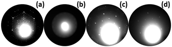
Figure 4.
LEED pattern of Si(111)-(7 × 7) surface (a). Diffraction image collected after deposition of 16 mL thick Au layer on clean Si substrate (b). LEED patterns corresponding to disintegrated Au layer deposited on both clean Si surface (c) and native Si oxide (d), collected at temperatures of 663 K and 857 K, respectively. The images were collected with electron energy of 33.7 eV (a), 14.2 eV (b), and 45.7 eV (c,d).
A comparison of the mechanisms responsible for the formation of nanometric Au islands on clean and oxidized Si surfaces was performed by observation of the annealing effect with an SEM. Gold thin film that evaporated on both types of substrates were annealed in a furnace for 15 min at temperatures in a range of 500 K up to 800 K, then cooled and images were obtained with an SEM. A strong dependence of the surface morphology of the samples on the annealing temperature and type of substrate can be observed on the SEM images presented in Figure 5. Observations for structures formed on pure silicon substrates are in line with the previous ones, as presented in Figure 3. However, the presence of native silicon oxide film drastically changes the effects of annealing. The obtained structures are much smaller and more spherical than the islands grown on deoxidized Si. There are two possible explanations of these differences. First, the surface tensions of gold on silicon and silicon oxide are different, which means that wetting by gold is more favorable on clean Si than on silicon oxide-covered substrate. In addition, the diffusion and exchange of species could be blocked at the Au-Si or Au-silicon oxide interface. It is well established already that enrichment of the gold film with silicon reduces the contact angle [41], which leads to the spreading of isolated Au-Si islands on the silicon surface instead of the formation of spherical droplets of pure gold.
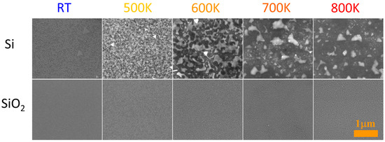
Figure 5.
SEM images of the 3 nm gold film deposited on silicon (111) (top panel) and silicon oxide substrates (bottom panel) and annealed for 15 min at various temperatures. Additionally, images of as-deposited (RT) films are presented. The scale bar is the same for all images.
In order to highlight the differences resulting from the various states of substrate surfaces, Figure 6 shows high-magnification SEM images of Au deposit after 15 min long annealing at 600 K. Additionally, Figure 7 presents similar SEM images of Au films annealed at 600 K for various times, from 5 min up to 15 min. As seen, for films deposited on the pure silicon surface an increase in annealing temperature results in the formation of bigger and more visible structures. EDS point measurements confirmed a perfect removal and agglomeration in the formation of nanoislands of gold. Additionally, triangular islands are visible, as a result of lateral growth of Si (111) structures [41,42]. On the contrary, for samples prepared on native silicon oxide film their surface morphology does not change significantly and hemispherical nanostructures are well-visible for each annealing time (Figure 7). For comparison, in Figure 8a the AFM image of well-formed nanostructures on a substrate with native oxide is presented. Nanoislands were formed as a result of annealing the 16 ML film up to 857 K during LEEM and LEED observations in a vacuum chamber. The obtained hemispherical nanoislands uniformly covered the whole substrate’s area. On the basis of AFM investigations, the average size of nanostructures was found to be ca. 80 nm in both horizontal and vertical axes. A histogram with a size distribution is shown in Figure 8b. The histogram was prepared on the basis of AFM observations. It can be seen that the nanostructures are significantly larger than those presented in Figure 6 and Figure 7. This is due to different annealing conditions. The heating rate was much smaller during LEEM and LEED observations than during annealing in a furnace. Finally, the heating took longer, which resulted in the formation of bigger structures. A strong influence of heating parameters on the size of nanostructures was observed in our previous works, e.g., [13,14,15].
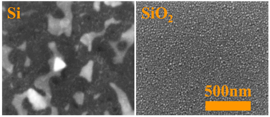
Figure 6.
SEM images of the 3 nm gold film deposited on clean silicon (111) (left panel) and silicon with native silicon oxide (right panel) substrates annealed for 15 min at 600 K. The scale bar is the same for both images.
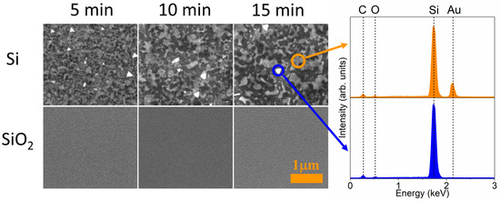
Figure 7.
SEM images of the 3 nm gold film deposited on silicon (111) and silicon oxide substrates and annealed for 5, 10, and 15 min at 600 K (left panel). Additionally, EDS point spectra are presented (right panel).
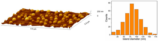
Figure 8.
AFM image of isolated gold nanoislands on a silicon with native oxide formed by the annealing of metallic thin film at temperature 857 K (left panel) and the island size histogram calculated for the same sample (right panel).
XPS method was used to determine the chemical composition and valence state of silicon and gold in structures. Both types of samples were measured and then evaporated on pure silicon and silicon with silicon oxide. The spectra were measured immediately after Au deposition (Figure 9a,b) and after annealing at 600 K (Figure 9c,d). For each structure, two characteristic, for metallic gold, peaks at 83.9 eV and 87.6 eV are visible. They correspond to Au4f5/2 and Au 4f7/2 signals. The positions and shapes of Au4f peaks seem to be similar for as-deposited films (spectra a and b), while for annealed samples some asymmetry on the high-energy side (at ca. 90 eV) can be noticed. It could be related to the additional gold–silicide compound that appears on a surface [43,44]. Its presence is obvious for structures formed on clean silicon due to silicon diffusion from the substrate. The presence of the Au-Si compound in samples with native oxide film could be explained by the etching of the oxide layer by liquid gold droplets, which was observed by LEED. Then, diffusion of Si atoms could start. Additionally, spectra for annealed samples exhibit the presence of a mix of metallic silicon and silicon oxide signals, with more metallic phases for structures evaporated on clean Si. The presence of silicon oxide in this case is related to fast oxidation in the air of the silicon surface.
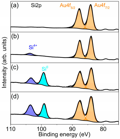
Figure 9.
High-resolution XPS spectra for Si2p and Au4f regions, recorded for: (a) 16 mL of gold evaporated on silicon substrate, (b) 16 mL of gold evaporated on silicon substrate with native oxide, (c) nanostructures obtained as a result of annealing at 600 K for 15 min of gold film deposited on Si, (d) nanostructures obtained as a result of annealing at 600 K for 15 min of gold film deposited on Si with native oxide.
On the basis of measurements and performed analysis, we described the mechanism of the disintegration of metallic thin films. It could be concluded that the process of the disintegration of gold films occurs in various modes, depending on the substrate. In the case of pure silicon substrates, interface diffusion could play a bigger role in the process than for substrates with native silicon oxide. Silicon dioxide is a well-known and widely used diffusion barrier [45]. One of our important new findings is that only the etching of the silicon oxide layer by liquid gold starts the diffusion process. It is reported that substrates play a key role in the process of the disintegration of metallic film, due to various surface tensions that have an influence on wetting properties [13,46,47]. The rate of diffusion must also be taken into account when considering the disintegration process. It is clear that the kind of substrate has an important influence on the size and shape of formed nanoislands. It could be useful for the design and production of optical active structures, where plasmonic properties strongly depend on nanostructure dimensions [48]. Our previous studies exhibit potential for tailoring plasmon resonance positions by change of, e.g., initial film thickness [13,14,15]. Here, we have shown an alternative method of changing the dimensions of the plasmonic structures.
4. Conclusions
Our microscopic and structural studies have shown various mechanisms of the disintegration of gold film on clean Si and Si with native oxide substrates. The disintegration of continuous film starts at a multiple grain junction, which was perfectly illustrated by LEEM. Thermal dewetting of the metallic thin films, deposited on both types of substrates, leads to the formation of nanoislands. However, the final shape and size of the islands strongly depends on the presence of native oxide on the silicon substrate. It was noticed that wetting of the deoxidized silicon substrate by gold is more preferable than in the case of the silicon oxide-covered substrate. Moreover, diffusion could be blocked by silicon oxide in the beginning phase of the disintegration of gold film. Additionally, an etching effect of the native silicon oxide by gold droplets was observed by LEED investigations and confirmed by XPS method.
Author Contributions
M.Ł.: conceptualization; methodology; data curation; formal analysis; investigation; validation; supervision; visualization; writing—original draft preparation; and writing—review and editing. P.D.: methodology; formal analysis; investigation; and writing—original draft preparation. M.G.: investigation. P.O.: investigation. J.K.: methodology and investigations. M.S.: methodology and investigations. A.P. investigation. Z.R.Z.: methodology and supervision. R.Z.: methodology and supervision. W.S.: supervision. B.K.: supervision and writing—review and editing. All authors have read and agreed to the published version of the manuscript.
Funding
This work was partially supported by the NCN grant 2021/43/D/ST7/01936 (M.S.) and by Gdańsk University of Technology by the DEC- 11/1/2022/IDUB/I3b/Ag grant under the ARGENTUM-‘Excellence Initiative-Research University’ program (M.Ł.).
Institutional Review Board Statement
Not applicable.
Informed Consent Statement
Not applicable.
Data Availability Statement
The data that support the findings of this study are available from the corresponding author upon reasonable request.
Acknowledgments
LEED and LEEM observations were performed during the scientific stay of M.Ł. at Maria Curie-Skłodowska University, Lublin. The stay was financially supported by the Division of Nanomaterials Physics, Institute of Nanotechnology and Materials Engineering, Gdansk University of Technology.
Conflicts of Interest
The authors declare no conflict of interest.
References
- Giermann, L.; Thompson, C.V. Solid-state dewetting for ordered arrays of crystallographically oriented metal particles. Appl. Phys. Lett. 2005, 86, 121903. [Google Scholar] [CrossRef]
- Wang, D.; Shaaf, P. Thermal dewetting of thin Au films deposited onto line-patterned substrates. J. Mater. Sci. 2012, 47, 1605–1608. [Google Scholar] [CrossRef]
- Ruffino, F.; Grimaldi, M.G. Self-organized patterned arrays of Au and Ag nanoparticles by thickness-dependent dewetting of template-confined films. J. Mater. Sci. 2014, 49, 5714–5729. [Google Scholar] [CrossRef]
- Preston, A.S.; Hughes, R.A.; Demille, T.B.; Rey Davila, V.M.; Neretina, S. Dewetted nanostructures of gold, silver, copper and palladium with enhanced faceting. Acta Mater. 2019, 165, 15–25. [Google Scholar] [CrossRef]
- Toliopoulos, D.; Fedorov, A.; Bietti, S.; Bollani, M.; Bonera, E.; Ballabio, A.; Isella, G.; Bouabdellaoui, M.; Abbarchi, M.; Tsukamoto, S.; et al. Solid-State Dewetting Dynamics of Amorphous Ge Thin Films on Silicon Dioxide Substrates. Nanomaterials 2020, 10, 2542. [Google Scholar] [CrossRef] [PubMed]
- Wakayama, Y.; Tagami, T.; Tanaka, S.I. Three-dimensional islands of Si and Ge formed on SiO2 through crystallization and agglomeration from amorphous thin films. Thin Solid Films 1999, 350, 300. [Google Scholar] [CrossRef]
- Cheynis, F.; Leroy, F.; Müller, P. Dynamics and instability of solid-state dewetting. Comptes Rendus Phys. 2013, 14, 578. [Google Scholar] [CrossRef]
- Thompson, C.V. Solid-State Dewetting of Thin Films. Annu. Rev. Mater. Res. 2012, 42, 399–434. [Google Scholar] [CrossRef]
- Atiya, G.; Chatain, D.; Mikhelashvili, V.; Eisenstein, G.; Kaplan, W.D. The role of abnormal grain growth on solid-state dewetting kinetics. Acta Mater. 2014, 81, 304–314. [Google Scholar] [CrossRef]
- Temmyo, J. Semiconductor Nanostructures, Self-organization of. In Encyclopedia of Materials: Science and Technology; Buschow, K.H.J., Cahn, R.W., Flemings, M.C., Ilschner, B., Kramer, E.J., Mahajan, S., Veyssière, P., Eds.; Elsevier: Amsterdam, The Netherlands, 2001; pp. 8335–8339. [Google Scholar]
- Danielson, D.T.; Sparacin, D.K.; Michel, J.; Kimerling, L.C. Surface-energy-driven dewetting theory of silicon-on-insulator agglomeration. J. Appl. Phys. 2006, 100, 083507. [Google Scholar] [CrossRef]
- Srolovitz, D.J.; Goldiner, M.G. The Thermodynamics and Kinetics of film agglomeration. JOM 1995, 47, 31–36. [Google Scholar] [CrossRef]
- Łapiński, M.; Kozioł, R.; Cymann, A.; Sadowski, W.; Kościelska, B. Substrate Dependence in the Formation of Au Nanoislands for Plasmonic Platform Application. Plasmonics 2020, 15, 101–107. [Google Scholar] [CrossRef]
- Kozioł, R.; Łapiński, M.; Syty, P.; Koszelow, D.; Sadowski, W.; Sienkiewicz, J.E.; Kościelska, B. Evolution of Ag nanostructures created from thin films: UV–vis absorption and its theoretical predictions. Beilstein J. Nanotechnol. 2020, 11, 494–507. [Google Scholar] [CrossRef] [PubMed]
- Kozioł, R.; Łapiński, M.; Syty, P.; Sadowski, W.; Sienkiewicz, J.E.; Nurek, B.; Maraloiu, V.A.; Kościelska, B. Experimental tuning of AuAg nanoalloy plasmon resonances assisted by machine learning method. Appl. Surf. Sci. 2021, 567, 150802. [Google Scholar] [CrossRef]
- Addab, Y.; Kini, M.K.; Courtois, B.; Savan, A.; Ludwig, A.; Bozzolo, N.; Scheu, C.; Dehm, G.; Chatain, D. Microstructure evolution and thermal stability of equiatomic CoCrFeNi films on (0001) α-Al2O3. Acta Materi. 2020, 200, 908–921. [Google Scholar] [CrossRef]
- Kaplan, W.D.; Chatain, D.; Wynblatt, P.; Carter, W.C. A review of wetting versus adsorption, complexions, and related phenomena: The rosetta stone of wetting. J. Mater. Sci. 2013, 48, 5681–5717. [Google Scholar] [CrossRef]
- Amram, D.; Klinger, L.; Gazit, N.; Gluska, H.; Rabkin, E. Grain boundary grooving in thin films revisited: The role of interface diffusion. Acta Mater. 2014, 69, 386–396. [Google Scholar] [CrossRef]
- Shaffir, E.; Riess, I.; Kaplan, W.D. The mechanism of initial de-wetting and detachment of thin Au films on YSZ. Acta Mater. 2009, 57, 248–256. [Google Scholar] [CrossRef]
- Ewing, G.E. Thin Film Water. J. Phys. Chem. B 2004, 108, 15953–15961. [Google Scholar] [CrossRef]
- Dai, C.; Saidi, P.; Song, H.; Yao, Z.; Daymond, M.R.; Hoyt, J.J. A test of a phenomenological model of size dependent melting in Au nanoparticles. Acta Mater. 2017, 136, 11–20. [Google Scholar] [CrossRef]
- Chen, J.; Fan, X.; Liu, J.; Gu, C.; Shi, Y.; Singh, D.J.; Zheng, W. Heating-Rate and Particle-Size Effects on Melting Process of Au Nanoparticles. J. Phys. Chem. C 2020, 124, 7414–7420. [Google Scholar] [CrossRef]
- Gapska, A.; Łapiński, M.; Syty, P.; Sadowski, W.; Sienkiewicz, J.E.; Kościelska, B. Au–Si plasmonic platforms: Synthesis, structure and FDTD simulations. Beilstein J. Nanotechnol. 2018, 9, 2599–2608. [Google Scholar] [CrossRef] [PubMed]
- Zhao, Z.J.; Ahn, J.; Ko, J.; Jeong, Y.; Bok, M.; Hwang, S.H.; Kang, H.-J.; Jeon, S.; Choi, J.; Park, I.; et al. Shape-Controlled and Well-Arrayed Heterogeneous Nanostructures via Melting Point Modulation at the Nanoscale. ACS Appl. Mater. Inter. 2021, 13, 3358–3368. [Google Scholar] [CrossRef]
- Chu, M.Z.; Zhang, C.; Liang, X.H.; Hu, C.H.; Ma, G.T.; Fang, R.Y.; Tang, C. Melting and phase diagram of Au-Cu alloy at nanoscale. J. Alloys Compd. 2022, 891, 162029. [Google Scholar] [CrossRef]
- Chu, M.Z.; Qin, Y.Z.; Xiao, T.; Shen, W.; Su, T.; Hu, C.H.; Tang, C. Thermodynamic reassessment of the Ag–Cu phase diagram at nano-scale. Calphad 2021, 72, 102233. [Google Scholar] [CrossRef]
- Gladkikh, N.T.; Bogatyrenko, S.I.; Kryshtal, A.P.; Anton, R. Melting point lowering of thin metal films (Me = In, Sn, Bi, Pb) in Al/Me/Al film system. Appl. Surf. Sci. 2003, 219, 338–346. [Google Scholar] [CrossRef]
- Bahloul-Hourlier, D.; Perrot, P. Thermodynamics of the Au-Si-O System: Application to the Synthesis and Growth of Silicon-Silicon dioxide Nanowires. J. Phs. Eqil Diff. 2007, 28, 150–157. [Google Scholar] [CrossRef]
- Wójcik, N.A.; Barczyński, R.J. The Influence of Thin Gold Electrodes on the High-Temperature Impedance of Oxide Glasses. Coatings 2022, 12, 784. [Google Scholar] [CrossRef]
- Łapiński, M.; Kozioł, R.; Zawadzka, A.; Sadowski, W.; Kościelska, B. Thermal dewetting as a method of surface modification of the gold thin films for surface plasmon resonance based sensor applications. Mater. Today Commun. 2022, 32, 104066. [Google Scholar] [CrossRef]
- Łapiński, M.; Synak, A.; Gapska, A.; Bojarski, P.; Sadowski, W.; Kościelska, B. New plasmonic platform for enhanced luminescence of valrubicin. Opt. Mater. 2018, 83, 225–228. [Google Scholar] [CrossRef]
- Łapiński, M.; Kozioł, R.; Syty, P.; Patela, S.; Sienkiewicz, J.E.; Sadowski, W.; Kościelska, B. Tuning of the plasmon resonance location in Au nanostructures coated with a ultrathin film of Al2O3–Optical measurements and FDTD simulations. Surf. Sci. 2023, 733, 122289. [Google Scholar] [CrossRef]
- Łapiński, M.; Kozioł, R.; Skubida, W.; Winiarz, P.; Elhassan, R.M.Y.; Sadowski, W.; Kościelska, B. Transformation of bimetallic Ag–Cu thin films into plasmonically active composite nanostructures. Sci. Rep. 2023, 13, 10107. [Google Scholar] [CrossRef] [PubMed]
- Kopciuszyński, M.; Zdyb, R.; Jałochowski, M. Influence of Si(111) surface superstructure on quantum size effect in Au films. Appl. Surf. Sci. 2014, 304, 40–43. [Google Scholar] [CrossRef]
- Jaroch, T.; Zdyb, R. Temperature-Dependent Growth and Evolution of Silicene on Au Ultrathin Films—LEEM and LEED Studies. Materials 2022, 15, 1610. [Google Scholar] [CrossRef] [PubMed]
- Święch, W.; Bauer, E.; Mundschau, B. A low-energy electron microscopy study of the system Si(111)-Au. Surf. Sci. 1991, 253, 283–296. [Google Scholar] [CrossRef]
- Jaroch, T.; Krawiec, M.; Zdyb, R. Layered Heterostructure of Planar and Buckled Phases of Silicene. 2D Mater. 2021, 8, 035038. [Google Scholar] [CrossRef]
- Hijazi, H.; Leroy, F.; Monier, G.; Grégoire, G.; Gil, E.; Trassoudaine, A.; Dubrovskii, V.G.; Castelluci, D.; Isik Goktas, N.; LaPierre, R.R.; et al. Dynamics of Gold Droplet Formation on SiO2/Si(111) Surface. J. Phys. Chem. C 2020, 124, 11946. [Google Scholar] [CrossRef]
- Naidich, Y.V.; Zhuravlev, V.; Krasovskaya, N. The wettability of silicon carbide by Au–Si alloys. Mater. Sci. Eng. A 1998, 245, 293–299. [Google Scholar] [CrossRef]
- Ressel, B.; Prince, K.C.; Heun, S.; Homma, Y. Wetting of Si surfaces by Au–Si liquid alloys. J. Appl. Phys. 2003, 93, 3886–3892. [Google Scholar] [CrossRef]
- Voigtländer, B.; Kawamura, M.; Paul, N.; Cherepanov, V. Formation of Si/Ge nanostructures at surfaces by self-organization. J. Phys. Condens. Matter. 2004, 16, S1535. [Google Scholar] [CrossRef]
- Kosolobov, S.S.; Aseev, A.L.; Latyshev, A.V. In Situ Study of Interaction of Oxygen with the Si(111) Surface by Ultrahigh-Vacuum Reflection Electron Microscopy. Semiconductors 2001, 35, 1038–1044. [Google Scholar] [CrossRef]
- Datta, D.P.; Siva, V.; Varma, S.; Kanjilal, D.; Sahoo, P.K. Ion induced dewetting of Au–Si on a SiO2 surface: Composite nanodot evolution and wettability transition. Phys. Chem. Chem. Phys. 2016, 18, 29955–29960. [Google Scholar] [CrossRef] [PubMed]
- Sahu, G.; Joseph, B.; Lenka, H.P.; Kuiri, P.K.; Pradhan, A.; Mahapatra, D.P. MeV Au irradiation induced nanoparticle formation and recrystallization in a low energy Au implanted Si layer. Nanotechnology 2007, 18, 495702. [Google Scholar] [CrossRef] [PubMed]
- Trempa, M.; Sturm, F.; Kranert, C.; Schanke, S.; Reimann, C.; Friedrich, J.; Schenk, C. Impact of different SiO2 diffusion barrier layers on lifetime distribution in multi-crystalline silicon ingots. J Cryst. Growth 2020, 532, 125378. [Google Scholar] [CrossRef]
- Pusztai, P.; Puskás, R.; Varga, E.; Erdőhelyi, A.; Kukovecz, Á.; Kónya, Z.; Kiss, J. Influence of gold additives on the stability and phase transformation of titanate nanostructures. Phys. Chem. Chem. Phys. 2014, 16, 26786–26797. [Google Scholar] [CrossRef]
- Chu, J.; Liu, X.; Zhang, X.; Zhang, J.; Xiao, J.; Chen, X.; Xu, J. Annealing temperature dependence of mechanical and structural properties of chromium-gold films on the silica glass substrate. Thin Solid Films 2023, 774, 139849. [Google Scholar] [CrossRef]
- Kang, M.; Park, S.G.; Jeong, K.H. Repeated Solid-state Dewetting of Thin Gold Films for Nanogap-rich Plasmonic Nanoislands. Sci. Rep. 2015, 5, 14790. [Google Scholar] [CrossRef]
Disclaimer/Publisher’s Note: The statements, opinions and data contained in all publications are solely those of the individual author(s) and contributor(s) and not of MDPI and/or the editor(s). MDPI and/or the editor(s) disclaim responsibility for any injury to people or property resulting from any ideas, methods, instructions or products referred to in the content. |
© 2023 by the authors. Licensee MDPI, Basel, Switzerland. This article is an open access article distributed under the terms and conditions of the Creative Commons Attribution (CC BY) license (https://creativecommons.org/licenses/by/4.0/).