Abstract
Lead-based ternary-chalcogenide thin films of the (PbTe)1−x(PbS)x system were obtained using the plasma-enhanced chemical-vapor-deposition (PECVD) technique under conditions of a nonequilibrium low-temperature argon plasma of an RF discharge (40.68 MHz) at a reduced pressure (0.01 Torr). High-purity elements were directly used as starting materials, namely Pb, S and Te. Plasma–chemical synthesis was carried out on the surface of c-sapphire and silicon substrate. The physicochemical properties of the films were studied using various analytical methods. The dependence of the Seebeck coefficient, resistivity and power factor on the structural properties and composition has been studied. The thermoelectric characteristics were found to be dependent on film composition. Upon the selection of optimal sulfur concentration, one can increase the power factor compared to single-phase PbS or PbTe films.
1. Introduction
Chalcogenide compounds are multifunctional materials with a number of practical applications. One can mention papers devoted to chalcogenides applications as mid-IR light detectors [1,2], photocatalytic materials [3,4,5,6] and thermoelectric power sources [7,8,9,10]. A set of the recent papers aimed to investigate thin-film lead ternary chalcogenides. The films were obtained via sputter deposition from a solution, physical vapor deposition, molecular beam and liquid phase epitaxy [11]. Among the mentioned techniques, the plasma-enhanced CVD (PECVD) method is distinguished by some unique capabilities, such as the possibility of depositing the film on any substrate (unlike epitaxial techniques) and compatibility with the whole set of standard lithography processes [12]. Previously, we have demonstrated the applicability of the PECVD technique for synthesizing complex chalcogenides [13,14].
The thermoelectric application of chalcogenides has been the subject of intense investigation since the 1950s [7]. Such interest is driven by a unique combination of electrical and thermal properties. Over the past 10 years, the number of publications on this subject has even tripled, for example [8,9,10]. Thermoelectricity implies the conversion of thermal energy into electrical energy when creating a temperature gradient (∆T) on opposite faces of a material. The value of thermo-voltage (UTE) in the case of a linear temperature gradient is given by the expression:
where is the Seebeck coefficient, which is a characteristic property of a material. The thermoelectric conversion efficiency is determined by the dimensionless thermoelectric figure of merit (ZT):
where T is the averaged temperature over the hot and cold faces of the sample, ρ is the resistivity and λ is the thermal conductivity.
A number of papers (e.g., [15,16,17]) report that thin films possess lowered thermal conductivity compared to their bulk counterparts. The Seebeck coefficient in thin films is, on the contrary, lower than that of bulk analogues. The general mechanism for the decrease in is a decrease in carrier mobility due to greater surface states’ contribution into carrier scattering [17,18,19]. However, the thermal conductivity decrease prevails the smaller , allowing one to achieve high values of ZT > 1. For that reason, the development of synthesis technologies for thin-film thermoelectric energy converters is considered an urgent task. In particular, great success has been achieved within bismuth telluride films, for example, in [20,21,22].
It should be emphasized that the output power of thin-film thermoelectric generators does not exceed the level of μW; thus, thin-film materials are mostly considered high-efficiency generators for low-power applications. For a comprehensive description of thin-film thermoelectric material efficiency, it is preferable to use the power factor (W) along with ZT as follows:
In the present paper, we mostly focus on investigating power factor W and its dependence on thin-film synthesis parameters.
From the point of view of thermoelectric applications, the most attractive representatives of AIVBVI compounds are PbS, PbSe and PbTe. Those are narrow-gap semiconductors with gap widths of 0.39 eV, 0.27 eV and 0.32 eV, respectively [23]. Such materials are usually considered low-temperature thermoelectric converters in a range of up to 500 K. One can cite a rather large number of papers devoted to the investigation of thermoelectric properties of either bulk [24,25] or thin-film [26,27,28,29,30] lead chalcogenides. Most recent papers are devoted to studying some approaches to improve the thermoelectric parameters of thin-film PbS or PbTe. Ref. [26] reports on the influence of oxidation on the ZT value, while ref. [29] is devoted to the investigation of the thickness dependence of the thermoelectric figure of merit. Some progress has been achieved through nanostructuring. For example, paper [27] has demonstrated an enhancement of the thermoelectric properties of films with incorporated PbSe quantum dots. In ref. [30], an increase in ZT value has been shown in film containing nano-size inclusions of the β-PbS2:Ga phase.
Despite noticeable progress in the development of thermoelectric chalcogenides, the practical implementation of such films is very limited. The main direction of further development is the modulation of the phase composition of the material by introducing additional atoms into the crystal lattice. In our previous work [31], we showed an increase in the power factor of PECVD-grown Pb0.05Se0.1Te0.85/Al2O3 film with respect to the PbTe/Al2O3 system. A similar approach has been discussed in a review paper [32]. The idea was developed towards an even more complicated PbTe-PbSe-PbS system. The initial results of such solutions were demonstrated for bulk nanocomposites with high doping levels [33]. The key feature of composition discussed is the extremely low thermal conductivity due to the mismatch of phonon spectra of the PbTe and PbS phases. The disadvantage of this approach was strong carrier scattering at the interphase boundaries, which led to a decrease in the Seebeck coefficient and an increase in resistivity. The result of an increase in ZT was unreasonably insignificant, taking into account technological difficulties in the synthesis of a four-component composition. The most breakthrough thermoelectric characteristics were obtained for (PbTe)z−x(PbSe)y(PbS)x pseudo-ternary compounds with a high ratio of PbS phase with respect to PbTe [7,8,9,10]. According to [10], the increase in (PbSe)y phase content up to y ~ 0.35 yields an increase in the equilibrium solubility limit of the PbS phase in PbTe. This approach yielded a great reduction in thermal conductivity; however, the abovementioned problem of interfacial carrier scattering causing a decrease in the Seebeck effect has not yet been solved.
The next step in improving the thermoelectric characteristics of lead chalcogenides might consist of a replacement of the PbSe phase by Pb-S-Te compounds. Such compounds are poorly discussed in the literature. Only a limited number of papers can be cited, for example, ref. [34], which is devoted to the investigation of mechanical properties of bulk PbSxTe1−x [35]. The phase diagram of such a composition has been studied in detail and presented, for example, in [7].
The thermoelectric properties of such compounds have not been investigated for either bulk or for thin-film materials to the best of our knowledge. The purposes of this work are to propose a new approach for the synthesis of (PbTe)1−x(PbS)x ternary lead chalcogenides and to establish the relationship between the growth parameters and thermoelectric properties of these materials.
2. Materials and Methods
A sketch of the experimental PECVD system is shown in Figure 1. The principle of operation of the set-up was described in detail in [13,14].
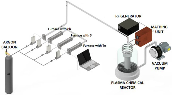
Figure 1.
Schematic of the plasma-enhanced CVD synthesis set-up.
The plasma–chemical reactor is a pear-shaped quartz vessel connected to a vacuum pumping system by a stainless-steel flange. An external inductor was placed on the narrow part of the plasma–chemical reactor. The reactor was equipped with a substrate holder made in the form of a cooled/heated pedestal for substrate positioning prior to film deposition. The substrate temperature in all experiments was about 15 °C.
The initial high-purity lead and chalcogens were loaded into quartz evaporators equipped with an external heater and a thermocouple for temperature control. Plasma-forming gas (Ar) was passed at a constant rate through evaporators heated above the melting point of the loaded precursors. The gas flow was set with high precision using gas-flow controllers. The amount and ratio of the reagents supplied to the plasma discharge were kept constant during the experiments. The deposition of (PbTe)1−x(PbS)x films was carried out under the following conditions: lead source temperature was 700 °C; sulfur temperature was 130 °C; tellurium temperature was 440 °C; total pressure in the reactor was 0.01 Torr; and total flow rate was 30 mL/min. The ratio of sulfur and tellurium in the grown films was controlled by changing the discharge power (60 W and 100 W). The precursor components were supplied into the reaction zone in the form of molecules (Pb, S8, Te2). Plasma discharge led to precursor atomization, resulting in better homogenization of grown film. Homogenization efficiency in turn depends on the discharge power.
The silicon (100) and c-sapphire (100) substrates with dimensions of 10 × 10 × 1 mm3 were used for film deposition. The purpose of the selection of these types of substrates is due to interest in studying the film growth under the following conditions:
(a) high lattice mismatch between both PbS and PbTe (4.936 Å, 6.460 Å) and silicon (5.430 Å);
(b) c-cut sapphire with a half-lattice parameter (6496 Å) almost matching PbTe but with large mismatch with PbS. A selection of sapphire substrates was additionally motivated by the task of separate consideration of (PbTe)1−x(PbS)x thermoelectric properties. The sapphire substrate was highly resistive, thus making no contribution to either entire system conductivity or the Seebeck coefficient. Low thermal conductivity of sapphire makes it possible to create sufficient values of the temperature gradient without the use of special tools for supplying and removing heat flux.
The chemical composition study of the fabricated samples was carried out by X-ray microanalysis using an X-MaxN 20 (Oxford Instruments, Japan, Kyoto) energy-dispersive elemental analysis set-up, implemented on the basis of JSM IT-300LV scanning electron microscope (JEOL), and by X-ray photoelectron spectroscopy (XPS) on an Omicron Multiprobe RM complex (Omicron Nanotechnology GmbH, Germany, Taunusstein). EDX measurements were carried out under conditions of high vacuum and an accelerating voltage of 20 kV.
To excite the emission of photoelectrons using the XPS technique, Mg Kα radiation was used. During the experiment, photoelectron lines were recorded as O 1s, C 1s, Pb 4f, Te 3d and S 2p. The analysis area diameter was 3 mm. The pressure of the residual gases was kept in the chamber at 5 × 10⁻⁹ mbar. To obtain information about the composition of the film, the surface of the layers was subjected to etching with Ar+ ions with an energy value of 1 kV. During this procedure, the pressure in the chamber was 4 × 10⁻⁶ mbar. The angle between the ion gun axis and the normal axis to the sample surface was 45°. The ion current registered on the sample during etching was 0.9 µA/cm2. The temperature of the sample during the entire experiment did not exceed 50–60 °C. The calculated thickness of the removed layer was about 2 nm.
The Seebeck coefficient was measured upon the controlled generation of a temperature gradient (ΔT) on the edges of the structure under study. The sample was placed on two independent graphite stoves (heater), and the heating of each was controlled independently using K-type control thermocouples, which were connected to TRM101-PID controllers (Figure 2). The free ends of the thermocouples were thermostatted in a vacuum connector with a stabilized temperature Troom.
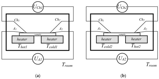
Figure 2.
Seebeck coefficient measurement scheme: the temperature gradient is created in the forward (a) and reverse directions (b), respectively.
The K-type measuring thermocouples (Chi, Ai) attached on top of the structures were used to record the resulting distribution of the thermal field. During the measurement process, the thermoelectric signal was recorded by measuring the voltage between the legs of chromel (UCh1) and alumel (UA1); this removed the parasitic contributions from the thermoelectric signal (Figure 2a). In order to take the asymmetry of the thermal contact between the tables into account, the same gradient of −ΔT was created in the opposite direction, and corresponding values of the thermopower UCh2 and UA2 were recorded (Figure 2b). The entire registration process was carried out in automatic mode using the L-CARD E14-140-MD data collection system. The measurement error of the Seebeck coefficient was ~5%. Detailed information on the Seebeck coefficient measurement can be found in [17,18,31].
The electrical resistance of the investigated thin films was also recorded by measuring the I-V characteristic with a classical two-contact circuit. Resistance recording was carried out upon keeping the temperatures of two stages equal. More details on the technique can be found in [17,18,34]. The measurement error for resistivity was ~1%.
The measurements of the Seebeck coefficient and resistivity were carried out in the temperature range of 50–275 °C. The power factor was calculated by Equation (3). The power factor calculation error was ~10%.
The concentration of carriers was measured by recording the magnetic field dependence of the Hall resistance. During these measurements a sample was placed into a magnetic field induced by an electromagnet. An electric current was passed through the sample and Hall resistance was recorded using a Keithley-2401 current source and voltage meter. The magnetic field was measured using an InSb-based Hall sensor using an L-Card E14-140MD data acquisition system. The measurements were carried out at 300 K. The concentration and mobility calculation error was ~3%.
3. Results and Discussion
3.1. Elemental Analysis and Scanning Electron Microscopy
The surface of all (PbTe)1−x(PbS)x samples was uniform, matte and gray. An increase in the sulfur content was accompanied by a change in the surface shade from dark gray to light gray (silver). The average layer thickness was 400–600 nm in the case of an average deposition time of 1 h.
Table 1 presents the results of X-ray microanalysis of thin-film samples depending on the plasma power and the type of substrate used. As can be seen from the data presented in Table 1, both the plasma power and the substrate material affect the macrocomposition of the fabricated films. An increase in the discharge power from 60 to 100 W led to an increase in sulfur content and, accordingly, to a decrease in tellurium content. The S content increases from 3 to 10 at.% for the sapphire substrate and from 5 to 12 at.% for the silicon substrate. Thus, samples grown on a silicon substrate include some higher ratio of sulfur compared to films grown under similar conditions on sapphire (with respect to the accuracy of the analytical method). Such an effect is probably due to the difference in Pb, Te and S incorporation efficiency in growing films driven by different lattice mismatches between Si(sapphire) and (PbTe)1−x(PbS)x.

Table 1.
Synthesis conditions and film compositions (PbTe)1−x(PbS)x.
The dependence of film composition on discharge power is believed to be due to the differences in the dissociation energies of the precursor components (Pb, S8, and Te2), resulting in different efficiencies of Pb, S8, and Te2 decomposition upon power modulation.
Figure 3a–d shows scanning electron microscopy images of (PbTe)1−x(PbS)x films on silicon and sapphire substrates. Grains with sharply defined edges are evenly distributed over the surface on all lead-based ternary-chalcogenide films. It should be emphasized that neither crack-type defects, detachments or point holes were revealed in the films. The presented SEM images yield the conclusion that the synthesized materials are polycrystalline, while the morphology of the resulting structures is affected by both the plasma power and the substrate material.
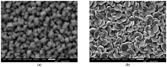
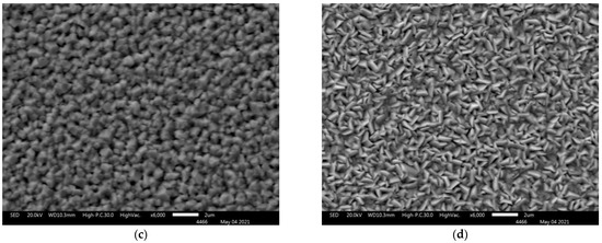
Figure 3.
SEM images of (PbTe)1−x(PbS)x films of various compositions: sample 1 (a), sample 2 (b), sample 3 (c), sample 4 (d).
With the plasma power increase, the average grain size decreased from 1 μm to 500 nm in the case of the sapphire substrate (Figure 3a,b correspondingly) and from 2 μm to 1 μm in the case of the silicon substrate (Figure 3c,d). Such an effect is attributed to the increase in the intensity of ion etching of the surface with plasma power increase. The ion etching leads to the removal of weakly bound fragments from the surface.
The EDX spectrum of the investigated (PbTe)0.76(PbS)0.24 film is shown in Figure 4a, and the corresponding XPES spectrum is shown in Figure 4b. In both spectra, the peaks corresponding to Pb, Te and Se are revealed. The EDX spectrum includes the lines of oxygen and Al, which is likely a signal from the Al2O3 substrate. The oxidation of Te and S can also be the origin of O line, which can be seen from the XPES data.
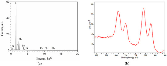
Figure 4.
The EDX (a) and XPS (b) spectra of investigated (PbTe)0.76(PbS)0.24 film.
Analysis of the Te 3d and S 2p photoelectronic lines using the procedure [36] and reference data from [37,38] allowed us to establish S-Pb and Te-Pb chemical bonds in the system, while the ratio of the concentrations of these bonds was 1 to 3, which is in good agreement with the EDX data. One should also note the presence of oxygen-containing S and Te bonds; the concentration of such compounds decreased sharply deep in the structure.
3.2. Results of XRD Phase Analysis
Figure 5b shows a distinctive XRD pattern for films of the (PbTe)1−x(PbS)x system. The films represent a two-phase system containing PbS and PbTe phases. To confirm this conclusion, Figure 5 shows the XRD curves for pure PbS (Figure 5a) and PbTe (Figure 5c).
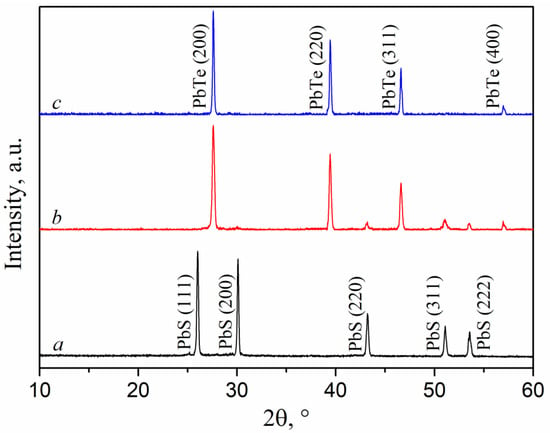
Figure 5.
XRD curves of (PbTe)1−x(PbS)x films on sapphire of various compositions: (a) PbS, (b) (PbTe)0.94(PbS)0.06, (c) PbTe. Standard pdf card for PbS is PDF#05-0592; for PbTe, it is DF#38-1435.
The orientation of lead telluride crystallites in the (200) direction remained unchanged after a small amount of sulfur was introduced. On the contrary, high tellurium content (x = 0.06) led to a change in the preferred PbS crystallite orientation from (111) for pure lead sulfide to (311) for (PbTe)1−x(PbS)x films. The lattice constants of PbS and PbTe were calculated using the standard formulae given, for example, in [39]. The obtained values were approximately 5.93 and 6.46 Å, respectively, which is in good agreement with the literature data.
These values are consistent with the literature data; moreover, they remain unchanged regardless of film composition. In addition, the PbTe phase was subjected to a decrease in the size of crystallites, an increase in the density of dislocations, and microdeformations upon the introduction of either tellurium into lead sulfide or sulfur into lead telluride. In particular, crystallite size decreased from about 45 to 30 nm, the dislocation density increased from 0.48 × 10¹⁵ to 0.97 × 10¹⁵ m−2, and microdeformation increased from 0.0071 to 0.0101. The dislocation density was calculated from XDR spectra using the technique described earlier in [39]. In the case of the PbS phase, reliable estimation of the crystallites’ parameters turned out to be complicated because of the very low intensity of the reflections observed. However, estimation of the (311) reflection half-width yielded an assumption that crystallite size also decreased.
The effect of substrate type on the diffraction patterns of (PbTe)1−x(PbS)x films is shown in Figure 6a,b. For both substrates under study, a two-phase system consisting of PbS and PbTe was revealed. However, in the case of the sapphire substrate, PbTe crystallites were predominantly oriented in the (200) direction, while for a film deposited on silicon, the (220) direction was dominant (Figure 6b). Another peculiarity revealed was a shift in the diffraction maxima from PbTe towards larger angles detected for the film grown on the silicon substrate. Such a shift indicates compression of the crystal lattice of lead telluride in comparison with the film grown on the sapphire substrate. The calculated lattice constants of crystallites in the PbTe films deposited on sapphire and silicon were 6.46 and 6.44 Å, respectively. The lattice parameter of PbS crystallites and their preferred orientation were, on the contrary, found to be independent on a substrate type. Finally, the sizes of the crystallites of both phases were slightly higher in films grown on the silicon substrate.
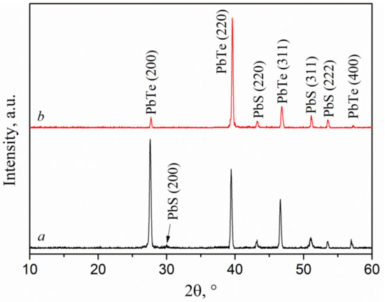
Figure 6.
XRD curves of (PbTe)1−x(PbS)x films deposited on sapphire with x = 0.06 (a) and silicon with x = 0.1 (b).
3.3. Thermoelectric Properties of the Films
One important condition for investigating the transport and thermoelectric characteristics of thin-film samples is the negligible electrical conductivity of the substrate. Otherwise, due to much greater thickness compared to the film, the substrate can make a decisive contribution to the properties under study [18]. The resistivity of the silicon substrate used was 3000 Ohm/cm2 and the thickness was 300 μm. The substrate resistance was thus 1000 Ohm/cm2, which is comparable with the resistance of the investigated film (>200 Ohm/cm2). Thus, in the case of a silicon substrate, shunting the thin-film layer upon heating is unavoidable. For this reason, the thermoelectric properties are further considered only for the films grown on sapphire. A series of samples with sulfur content varying from 0 at.% to 15 at.% was fabricated. The list of the investigated samples is presented in Table 2.

Table 2.
List of studied films grown on sapphire with indication of transport parameters at T = 300 K.
The mobility and concentration of carriers in the films under study were calculated from the magnetic field dependence of the Hall resistance (Table 2). Film thickness was estimated using atomic force microscopy by measuring the step height at the boundary of the sapphire surface covered and uncovered with a film. Such a step is usually formed within the film growth process because the material is not being deposited on the area shadowed by a substrate holder. The measured thickness of the films was 0.5 ± 0.1 μm.
From the magnetic field dependence of the Hall Effect, it was found that all films were of p-type conductivity. From the data in Table 2, it can be seen that the introduction of sulfur led to a decrease in the resistivity of the film. An increase in sulfur concentration was accompanied with an increase in carrier concentration. This is believed to be due to the high sensitivity of the PbS phase to electrically active defects, which are the source of additional holes [40]. The carrier mobility in sample 1 significantly exceeded the values obtained for samples 2–4, which is associated with additional carrier scattering at interfaces.
The measured temperature dependences of resistivity and the Seebeck coefficient are shown in Figure 7a,b, respectively. The measured values were used to calculate the temperature dependences of a power factor (Figure 7c). From the temperature dependence of resistivity (Figure 7a), it can be seen that all structures demonstrated a semiconductor nature of conductivity, i.e., the resistance decreased with the increase in temperature. A maximum temperature dependence of the Seebeck coefficient in the range of 75–175 °C was revealed for the entire batch.
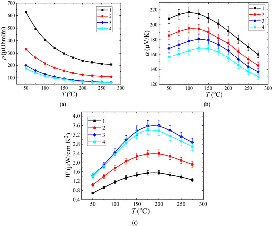
Figure 7.
Experimentally obtained temperature dependences of resistivity (a), Seebeck coefficient (b), power factor (c).
The value of the Seebeck coefficient was positive over the entire measured temperature range. This is consistent with the p-type conductivity revealed from the Hall effect measurement. The decrease in the Seebeck coefficient at high temperatures is associated with an increased contribution of intrinsic conductivity. The absolute values of the Seebeck coefficient correlate well with the resistivity value for all samples. For example, sample 1, possessing the highest resistivity among the batch (Figure 7a line 1), demonstrated the highest-value Seebeck coefficient in the entire temperature range (Figure 7b line 1). In sample 4, the lowest resistivity was accompanied with the lowest Seebeck coefficient (Figure 7a,b correspondingly). Resistivity was found to depend nonmonotonically on the sulfur content in the films. Sulfur content increased from 0 at.% (sample 1) to 5 at.% (sample 2) and led to a sharp decrease in resistivity (Figure 7a, lines 1 and 2). A further increase in sulfur content to 15 at.% led to much smaller decrease in resistivity (Figure 7a, lines 3 and 4).
Similar behavior was revealed for the temperature dependence of the Seebeck coefficient (Figure 7b). We should note that the sulfur content also affected the position of the Seebeck coefficient maximum on temperature dependence. In sample 1, the maximal Seebeck coefficient was obtained at 100 °C (Figure 7a line 1), while in sample 4, the maximum point was 150 °C (Figure 7a line 4). Such a shift is attributed to the increasing contribution of the PbS phase to the current transfer through the film. It is known from [23] that the PbS bandgap is by 70 meV higher than that of PbTe. Thus, PbS incorporation into PbTe yielded not only an increase in the thermoelectric power factor, but also a shift in the operating temperature range towards higher temperatures.
The highest power factor value of W ~ 3.6 μW/cm2·K was obtained in sample 3, which included 10 at.% of sulfur (Figure 7d line 3). The obtained maximum value of the power factor exceeds the values reported in [31]. The decrease in sulfur content to 5 at.% in sample 2 led to decrease in the power factor compared to the 10 at.% sample. The Seebeck coefficient increase (Figure 7a line 2) was fully compensated by a great increase in resistivity (Figure 7c line 2). Single-phase PbTe sample 1 was characterized by the lowest power factor among the batch (Figure 7c line 1), which was due to a greatly increased resistivity value (Figure 6a line 1). Thus, it is shown that a two-phase thin film can possess enhanced thermoelectric characteristics compared to a homogeneous single-phase film, despite the additional role of interfacial carrier scattering. An even greater increase in sulfur content up to 15 at.% yielded a further decrease in resistivity (Figure 7a line 4). However, this was accompanied by an even greater reduction in Seebeck coefficient (Figure 7b line 4), which in total led to a power factor decrease (Figure 7d line 4). A decrease in mobility and an increase in the carrier concentration can also be noted (Table 2).
Table 3 compares the maximum value of the power factor of sample 1 (PbTe) with a number of data from the literature for samples with a comparable composition and doping level.

Table 3.
Comparison of the power factor of sample 1 with literature data.
From Table 3, it can be seen that the data obtained are in good agreement with the literature, which indicates the reliability of the results obtained. Therefore, there is an optimum sulfur concentration that yields the highest power factor values. Further optimization of the thermoelectric figure of merit in such films can be achieve the introduction of a dopant.
4. Conclusions
The semiconductor (PbTe)1−x(PbS)x layers were grown on sapphire and silicon substrates. Structural investigation of the fabricated layers was carried out. The features of (PbTe)1−x(PbS)x film growth on sapphire substrates were shown; in particular, an investigation of the temperature dependences on the thermoelectric properties of the films was carried out. A strong influence of the stoichiometric composition both on the type of structure and the thermoelectric properties was shown.
Author Contributions
Investigation, writing—review and editing, Y.M.K.; Conceptualization and resources, L.A.M.; Supervision, M.V.D.; writing—original draft preparation, D.G.F., M.A.K., Y.P.K., I.L.K. and R.N.K.; Investigation, A.V.Z. and D.A.Z. All authors have read and agreed to the published version of the manuscript.
Funding
The work was supported by the Ministry of Science and Higher Education of the Russian Federation [FSWR-2023-0024]. X-ray microanalysis and scanning electron microscopy were performed using the equipment of the Center for Collective Usage “New Materials and Resource-Saving Technologies” (Research Institute of Chemistry, Lobachevsky State University of Nizhny Novgorod).
Institutional Review Board Statement
Not applicable.
Informed Consent Statement
Not applicable.
Data Availability Statement
Data presented in this article are available upon request from the corresponding author.
Conflicts of Interest
The authors declare no conflict of interest.
References
- Wang, B.; Zhong, S.P.; Zhang, Z.B.; Zheng, Z.Q.; Zhang, Y.P.; Zhang, H. Broadband photodetectors based on 2D group IVA metal chalcogenides semiconductors. Appl. Mater. Today 2019, 15, 115–138. [Google Scholar] [CrossRef]
- Xu, Y.; Li, R.; Bai, S.; Li, Y.; Jia, Z.; Yang, Y.; Cui, E.; Yao, F.; Wang, D.; Lei, C.; et al. Chalcogenide-based narrowband photodetectors for imaging and light communication. Adv. Funct. Mater. 2022, 33, 2212523. [Google Scholar] [CrossRef]
- Tayyab, M.; Liu, Y.; Liu, Z.; Xu, Z.; Yue, W.; Zhou, L.; Lei, J.; Zhang, J. A new breakthrough in photocatalytic hydrogen evolution by amorphous and chalcogenide enriched cocatalysts. Chem. Eng. J. 2023, 455, 140601. [Google Scholar] [CrossRef]
- Tshimangadzo, S.M.; Philiswa, N.N. Review on metal chalcogenides and metal chalcogenide-based nanocomposites in photocatalytic applications. Chem. Afr. 2023, 19, e01509. [Google Scholar]
- Ali, S.A.; Ahmad, T. Chemical strategies in molybdenum-based chalcogenides nanostructures for photocatalysis. Int. J. Hydrog. Energy 2022, 47, 29255–29283. [Google Scholar] [CrossRef]
- Li, J.; Jimenez-Calvo, P.; Paineau, E.; Ghazzal, M.N. Metal chalcogenides-based heterojunctions and novel nanostructures for photocatalytic hydrogen evolution. Catalysts 2020, 10, 89. [Google Scholar] [CrossRef]
- Yamini, S.A.; Wang, H.; Gibbs, Z.M.; Pei, Y.; Dou, S.X.; Snyder, G.J. Chemical composition tuning in quaternary p-type Pb-chalcogenides—A promising strategy for enhanced thermoelectric performance. Phys. Chem. Chem. Phys. 2014, 16, 1835–1840. [Google Scholar] [CrossRef]
- Yamini, S.A.; Wang, H.; Gibbs, Z.M.; Pei, Y.; Mitchell, D.R.G.; Dou, S.X.; Snyder, G.J. Thermoelectric performance of tellurium-reduced quaternary p-type lead–chalcogenide composites. Acta Mater. 2014, 80, 365–372. [Google Scholar] [CrossRef]
- Yamini, S.A.; Patterson, V.; Santos, R. Band-gap nonlinearity in lead chalcogenide (PbQ, Q = Te, Se, S) alloys. ACS Omega 2017, 2, 3417–3423. [Google Scholar] [CrossRef]
- Manettas, A.; Santos, R.; Ferreres, X.R.; Yamini, S.A. Thermoelectric performance of single-phase p-type quaternary (PbTe)0.65−x(PbSe)0.35(PbS)x alloys. ACS Appl. Energy Mater. 2018, 1, 1898–1903. [Google Scholar] [CrossRef]
- Hone, F.G.; Ampong, F.K.; Nkum, R.K.; Boakye, F. Band gap engineering in lead sulphur selenide (PbS1−xSex) thin films synthesized by chemical bath deposition method. J. Mater. Sci. Mater. Electron. 2017, 28, 2893–2900. [Google Scholar]
- Kudryashov, M.; Mochalov, L.; Nezdanov, A.; Kornev, R.; Logunov, A.; Usanova, D.; Mashin, A.; De Filpo, G.; Gogova, D. A novel plasma-based method for synthesis of As-Se-Te films: Impact of plasma parameters on the structure, composition, and optical properties. Superlattices Microstruct. 2019, 128, 334–341. [Google Scholar] [CrossRef]
- Mochalov, L.; Logunov, A.; Prokhorov, I.; Sazanova, T.; Kudrin, A.; Yunin, P.; Zelentsov, S.; Letnianchik, A.; Starostin, N.; Boreman, G.; et al. Plasma-chemical synthesis of lead sulphide thin films for near-IR photodetectors. Plasma Chem. Plasma Process. 2020, 41, 493. [Google Scholar] [CrossRef]
- Mochalov, L.; Logunov, A.; Markin, A.; Kitnis, A.; Vorotyntsev, V. Characteristics of the Te-based chalcogenide films dependently on the parameters of the PECVD process. Opt. Quantum Electron. 2020, 52, 197. [Google Scholar] [CrossRef]
- Kumanek, B.; Janas, D. Thermal conductivity of carbon nanotube networks: A review. J. Mater. Sci. 2019, 54, 7397–7427. [Google Scholar] [CrossRef]
- Tambasov, I.A.; Voronin, A.S.; Evsevskaya, N.P.; Kuznetsov, Y.M.; Luk’yanenko, A.V.; Tambasova, E.V.; Gornakov, M.O.; Dorokhin, M.V.; Loginov, Y.Y. Experimental study of the thermal conductivity of single-walled carbon nanotube-based thin films. Phys. Solid State 2020, 6, 1090–1094. [Google Scholar] [CrossRef]
- Dorokhin, M.V.; Kuznetsov, Y.M.; Lesnikov, V.P.; Zdoroveishchev, A.V.; Demina, P.B.; Erofeeva, I.V. Studies of thermoelectric properties of superlattices based on manganese silicide and germanium. Phys. Solid State 2019, 12, 2348–2352. [Google Scholar] [CrossRef]
- Erofeeva, I.V.; Dorokhin, M.V.; Lesnikov, V.P.; Kuznetsov, Y.M.; Zdoroveyshchev, A.V.; Pitirimova, E.S. Thermoelectric effects in nanoscale layers of manganese silicide. Semiconductors 2017, 11, 1403–1408. [Google Scholar] [CrossRef]
- Orlova, D.S.; Rogacheva, E.I. Galvanomagnetic properties of thin films of bismuth, doped with tellurium. Nanosyst. Nanomater. Nanotech. 2009, 2, 487–493. (In Russian) [Google Scholar]
- Park, N.-W.; Lee, W.-Y.; Yoon, Y.-S.; Kim, G.-S.; Yoon, Y.-G.; Lee, S.-K. Achieving out-of-plane thermoelectric figure of merit ZT = 1.44 in a p-type Bi2Te3/Bi0.5Sb1.5Te3 superlattice film with low interfacial resistance. ACS Appl. Mater. Interfaces 2019, 11, 38247–38254. [Google Scholar] [CrossRef]
- Zheng, Z.-H.; Shi, X.-L.; Ao, D.-W.; Liu, W.-D.; Li, M.; Kou, L.-Z.; Chen, Y.-X.; Li, F.; Wei, M.; Liang, G.-X.; et al. Harvesting waste heat with flexible Bi2Te3 thermoelectric thin film. Nat. Sustain. 2022, 6, 180–191. [Google Scholar] [CrossRef]
- Zheng, D.; Jin, H.; Liao, Y.; Ji, P. Bi2Te3 nanowires tuning PEDOT:PSS structure for significant enhancing electrical transport property. Mater. Lett. 2023, 338, 134019. [Google Scholar] [CrossRef]
- Lach-hab, M.; Papaconstantopoulos, D.A.; Mehl, M.J. Electronic structure calculations of lead chalcogenides PbS, PbSe, PbTe. J. Phys. Solids 2002, 63, 833–841. [Google Scholar] [CrossRef]
- Pei, Y.; LaLonde, A.; Iwanaga, S.; Snyder, G.J. High thermoelectric figure of merit in heavy hole dominated PbTe. Energy Environ. Sci. 2011, 4, 2085–2089. [Google Scholar] [CrossRef]
- Heremans, J.P.; Jovovic, V.; Toberer, E.S.; Saramat, A.; Kurosaki, K.; Charoenphakdee, A.; Yamanaka, S.; Snyder, G.J. Enhancement of thermoelectric efficiency in PbTe by distortion of the electronic density of states. Science 2008, 321, 554–557. [Google Scholar] [CrossRef] [PubMed]
- Rogacheva, E.I.; Krivulkin, I.M.; Nashchekina, O.N.; Sipatov, A.Y.; Volobuev, V.V. Effect of oxidation on the thermoelectric properties of PbTe and PbS epitaxial films. Appl. Phys. Lett. 2001, 78, 1661–1663. [Google Scholar] [CrossRef]
- Yang, D.; Lu, C.; Yin, H.; Herman, I.P. Thermoelectric performance of PbSe quantum dot films. Nanoscale 2013, 5, 7290–7296. [Google Scholar] [CrossRef]
- Yan, Q.; Chen, H.; Zhou, W.; Hng, H.H.; Boey, F.Y.C.; Ma, J. A simple chemical approach for PbTe nanowires with enhanced thermoelectric properties. Chem. Mater. 2008, 20, 6298–6300. [Google Scholar] [CrossRef]
- Rogacheva, E.I.; Nashchekina, O.N.; Vekhov, Y.O.; Dresselhaus, M.S.; Cronin, S.B. Effect of thickness on the thermoelectric properties of PbS thin films. Thin Solid Films 2003, 423, 115–118. [Google Scholar] [CrossRef]
- Geethu, R.; Jacob, R.; Shripathi, T.; Okram, G.S.; Ganesan, V.; Tripathi, S.; Fatima, A.; Sreenivasan, P.V.; Urmila, K.S.; Pradeep, B.; et al. Optoelectronic and thermoelectric properties in Ga doped β-PbS2 nanostructured thin films. Appl. Surf. Sci. 2012, 258, 6257–6260. [Google Scholar] [CrossRef]
- Mochalov, L.A.; Kuznetsov, Y.M.; Dorokhin, M.V.; Fukina, D.G.; Knyazev, A.V.; Kudryashov, M.A.; Kudryashova, Y.P.; Logunov, A.A.; Mukhina, O.V.; Zdoroveyshchev, A.V.; et al. Thermoelectrical properties of ternary lead chalcogenide plumbum-selenium-tellurium thin films with excess of tellurium prepared by plasma-chemical vapor deposition. Thin Solid Films 2020, 752, 139244. [Google Scholar] [CrossRef]
- Chen, X.; Zhou, Z.; Lin, Y.-H.; Nan, C. Thermoelectric thin films: Promising strategies and related mechanism on boosting energy conversion performance. J. Mater. 2020, 6, 494–512. [Google Scholar] [CrossRef]
- Ibanez, M.; Zamani, R.; Gorsse, S.; Fan, J.; Ortega, S.; Cadavid, D.; Morante, J.R.; Arbiol, J.; Cabot, A. Core-shell nanoparticles as building blocks for the bottom-up production of functional nanocomposites: PbTe-PbS thermoelectric properties. ACS Nano. 2013, 7, 2573–2586. [Google Scholar] [CrossRef] [PubMed]
- Dorokhin, M.V.; Kuznetsov, Y.M.; Demina, P.B.; Erofeeva, I.V.; Zavrazhnov, A.Y.; Boldin, M.S.; Lantsev, E.A.; Popov, A.A.; Boryakov, A.V.; Zdoroveyshchev, A.V.; et al. High-efficiency spark plasma sintered Ge0.3Si0.7:P thermoelectric energy converters with silicone phosphide as a source of phosphorus doping. Nanoscale Microscale Thermophys. Eng. 2023, 27, 125–134. [Google Scholar] [CrossRef]
- Othman, M.S. Mechanical response of PbSSe, PbSTe ternary and PbSnSTe quaternary alloys at high pressure. ARO-Sci. J. Koya Univ. 2020, 8, 29–33. [Google Scholar] [CrossRef]
- Boryakov, A.V.; Surodin, S.I.; Kryukov, R.N.; Nikolichev, D.E.; Zubkov, S.Y. Spectral fit refinement in XPS analysis technique and its practical applications. J. Electron Spectrosc. Relat. Phenom. 2018, 50, 1443–1448. [Google Scholar] [CrossRef]
- Crist, B.V. Handbooks of Monochromatic XPS Spectra: The Elements and Native Oxides; XPS International Inc.: Ames, IA, USA, 1999; Volume 1. [Google Scholar]
- Crist, B.V. Handbooks of Monochromatic XPS Spectra: Commercially Pure Binary Oxides and a Few Common Carbonates and Hydroxides; XPS International LLC: Mountain View, CA, USA, 2005; Volume 2. [Google Scholar]
- Shyju, T.S.; Anandhi, S.; Sivakumar, R.; Gopalakrishnan, R. Studies on lead sulfide (PbS) semiconducting thin films deposited from nanoparticles and Its NLO application. Int. J. Nanosci. 2014, 1, 1450001. [Google Scholar] [CrossRef]
- Li, W.; Fang, C.; Dijkstra, M.; Huis, M. The role of point defects in PbS, PbSe and PbTe: A first principles study. J. Phys. Condens. Matter. 2015, 27, 355801. [Google Scholar] [CrossRef]
- Bala, M.; Gupta, S.; Tripathi, T.S.; Varma, S.; Tripathi, S.K.; Asokan, K.; Avasthi, D.K. Enhancement of thermoelectric power of PbTe:Ag nanocomposite thin films. RSC Adv. 2015, 5, 33. [Google Scholar] [CrossRef]
- Gupta, S.; Agarwal, D.C.; Tripathi, S.K.; Neeleshwar, S.; Panigrahi, B.K.; Jacquot, A.; Lenoir, B.; Avasthi, D.K. Superiority of ion irradiation over annealing for enhancing the thermopower of PbTe thin films. Radiat. Phys. Chem. 2013, 86, 6–9. [Google Scholar] [CrossRef]
- Karthikeyan, V.; Surjadi, J.U.; Wong, J.C.K.; Kannan, V.; Lam, K.-H.; Chen, X.; Lu, Y.; Roy, V.A.L. Wearable and flexible thin film thermoelectric module for multi-scale energy harvesting. J. Power Sources 2020, 455, 227983. [Google Scholar] [CrossRef]
- Ahmad, K.; Almutairi, Z.; Wan, C. Thermoelectric properties of PbTe-based graphene nanocomposite. J. Mater. Sci. Mater. Electron. 2020, 31, 20996–21004. [Google Scholar] [CrossRef]
Disclaimer/Publisher’s Note: The statements, opinions and data contained in all publications are solely those of the individual author(s) and contributor(s) and not of MDPI and/or the editor(s). MDPI and/or the editor(s) disclaim responsibility for any injury to people or property resulting from any ideas, methods, instructions or products referred to in the content. |
© 2023 by the authors. Licensee MDPI, Basel, Switzerland. This article is an open access article distributed under the terms and conditions of the Creative Commons Attribution (CC BY) license (https://creativecommons.org/licenses/by/4.0/).