Article

High-Performance Ultra-Broadband Absorber for Polarized Long-Wavelength Infrared Light Trapping

1
Key Laboratory of Optical System Advanced Manufacturing Technology, Changchun Institute of Optics, Fine Mechanics and Physics, Chinese Academy of Sciences, Changchun 130033, China
2
University of Chinese Academy of Sciences, Beijing 100039, China
3
School of Optoelectronic Science and Engineering, Science and Technology, Soochow University, Suzhou 215006, China
4
Collaborative Innovation Center of Suzhou Nano, Science and Technology, Soochow University, Suzhou 215006, China
5
Key Lab of Advanced Optical Manufacturing Technologies of Jiangsu Province, Soochow University, Suzhou 215006, China
6
Key Lab of Modern Optical Technologies of Education Ministry of China, Soochow University, Suzhou 215006, China
*
Author to whom correspondence should be addressed.
Coatings 2022, 12(8), 1194; https://doi.org/10.3390/coatings12081194
Submission received: 16 July 2022 / Revised: 10 August 2022 / Accepted: 11 August 2022 / Published: 16 August 2022
(This article belongs to the Section Plasma Coatings, Surfaces & Interfaces)

Abstract

:
Conventional infrared polarization imaging and detection systems are normally complex, bulky, and expensive, since rare existing absorber components possess polarization selectivity, especially in the long-wavelength infrared (LWIR) range. In this study, we propose a novel high-performance metamaterial absorber with ultra-broadband high absorption and polarization selectivity in the entire LWIR atmospheric window. The absorber can realize an absorptance higher than 90% with a 4750 nm bandwidth due to different surface plasmons coupled with optical phonons. It exhibits precise polarization-selective absorption at the target wavelength; specifically, it can selectively trap TM-polarized light while restricting the absorption of TE-polarized light. In addition, the designed metamaterial exhibits remarkable spectral stability when the geometric parameters of the microstructure change, which is of great benefit in its manufacturing process. The proposed ultra-thin absorber provides a promising approach to simplify LWIR imaging and detection systems and further improve their performance.

Graphical Abstract

1. Introduction

Metamaterials are artificially constructed periodic sub-wavelength microstructures that can effectively manipulate the phase, amplitude, and polarization of electromagnetic waves and achieve novel functions that are not available in natural materials [1,2,3]. In general, surface plasmons (SPs) can be excited when electromagnetic waves are incident on a microstructure and can be categorized into propagating surface plasmons (PSPs) at the metal–dielectric interface and localized surface plasmons (LSPs) around metallic nanostructures [4]. The optical properties of SPs can be modulated by the shape, size, and material of the microstructures. Metamaterials based on SPs have achieved a variety of novel physical characteristics, such as negative refraction [5,6], negative reflection [7], super-resolution [8], metalens [9,10], and a zero refractive index [11]. This is significant in the design of plasmonic devices and has important applications in many fields, such as optical stealth [12], holography [13,14], optical communication [15], and sensing [16].
In recent years, absorbers based on metamaterials have been extensively investigated [17,18]. Metamaterial absorbers can selectively absorb incident electromagnetic waves at the nanoscale and modulate key parameters such as the response band, transmittance, and intensity [19,20], breaking through the limitations of conventional absorbers and triggering promising applications in detectors [21], thermal emitters [22], thermal imaging [23,24], and energy harvesting [25]. Previous research investigated the design of various structures to improve absorptance, including metal gratings [26,27], multilayer structures [28,29], nanoparticles [30], nanocubes [21], and nanoholes [31,32]. However, these studies usually focus on broadening the absorption peak and are insufficient for meeting the growing demand of polarization imaging. Conventional polarization imaging technologies pair pixels of an uncooled focal plane array with polarizers and place a 2 × 2 array of polarizers in front of a unit consisting of four pixels (the transmission axis of each polarizer is placed at 0°, 45°, 90°, and 135°) to measure intensity [33]. Nevertheless, additional polarizers make the optical system inevitably complex and bulky, leading not only to high costs but also to the degradation of the detector’s performance. Furthermore, in the long-wavelength infrared (LWIR) atmospheric window of 8000–14,000 nm, there are very few reports on polarization-selective absorbers. Designing an ultra-broadband high-absorption and polarization-selective absorber covering the entire LWIR is consequently necessary.
In this paper, we propose a novel high-performance metamaterial absorber. Compared with conventional absorbers, our absorber can simultaneously achieve ultra-broadband high absorption and polarization selectivity in the entire LWIR atmospheric window. First, we designed a metal-insulator-metal (MIM) absorber with grating resonators and adopted a high-optical-loss metal, chromium (Cr), as the resonators and bottom to achieve relatively narrow, single-peak absorption of TM-polarized light. In the designed microstructure, we observed the phenomena of propagating surface plasmon resonance (PSPR) and localized surface plasmon resonance (LSPR). Furthermore, we investigated a high-performance absorber with a three-layer stack dielectric: silicon nitride (Si3N4)-silicon (Si)-silicon nitride (Si3N4). It presented high absorption, ultra-broadband, and polarization selectivity, as the PSPs and LSPs excited by the resonance of the MIM absorber are coupled to the optical phonons of high-dispersion dielectrics. In addition, we found that the absorber possesses excellent spectral stability when adjusting the geometric parameters of the microstructure, which is beneficial to its manufacturing process.

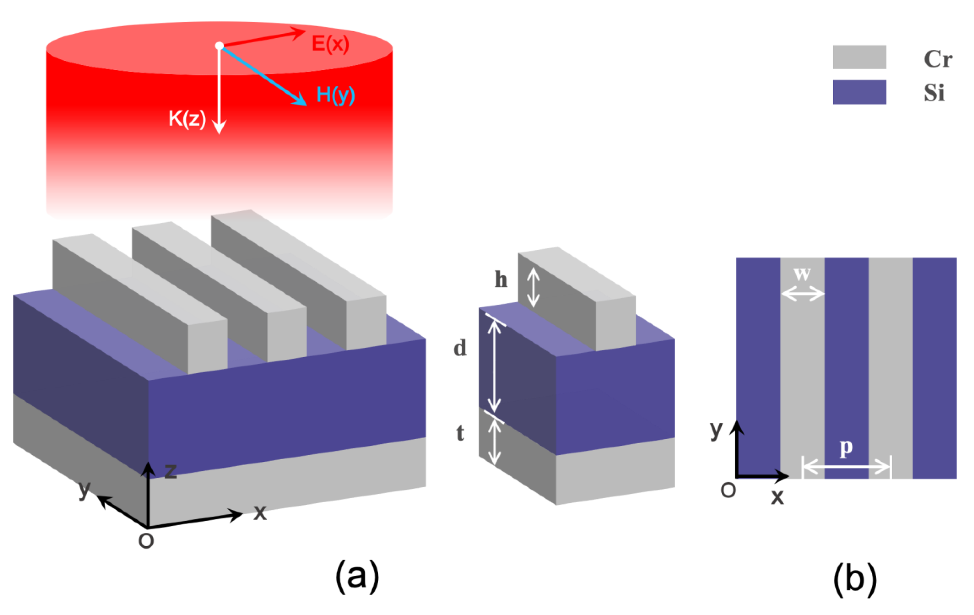
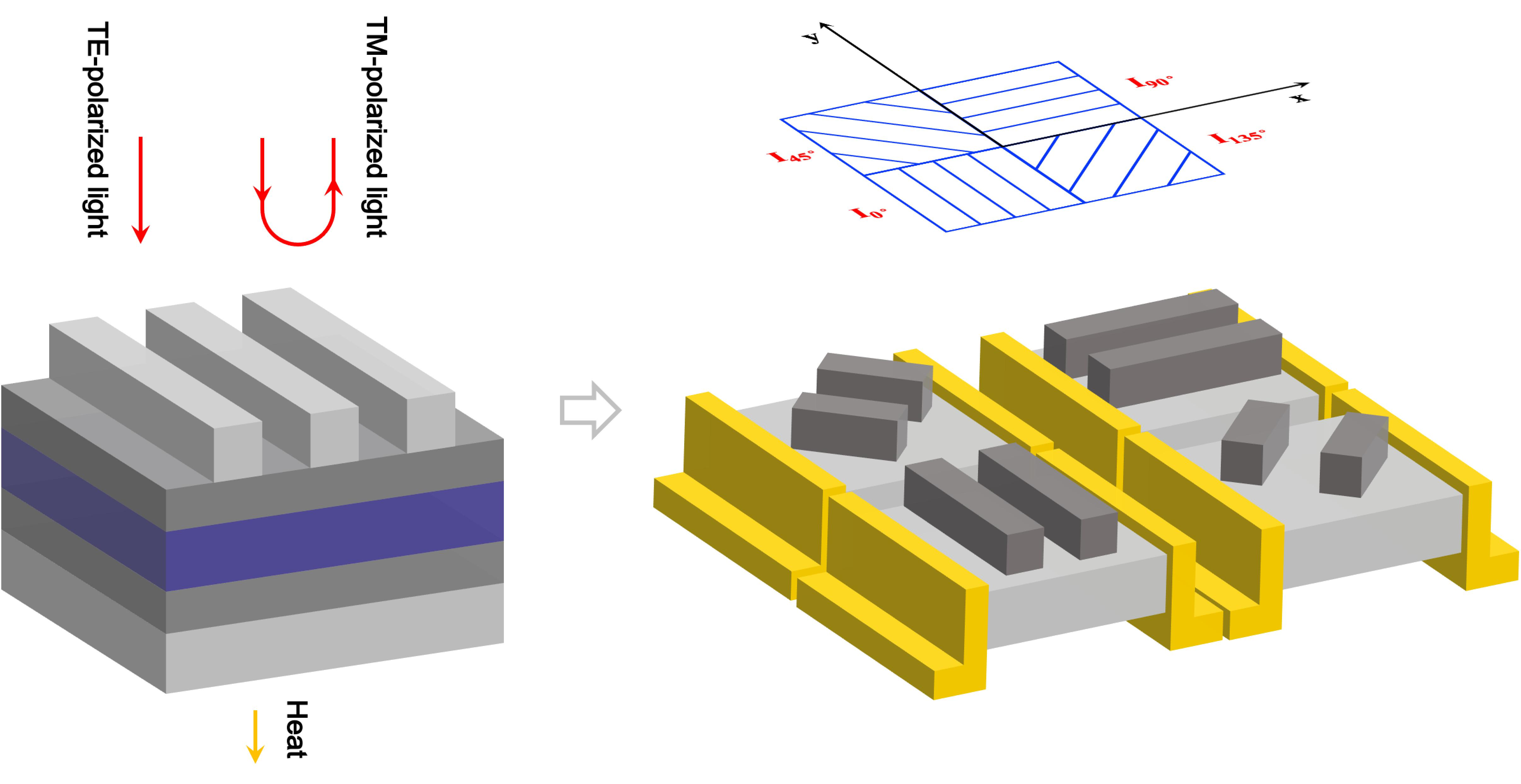
2. Structural Design and Methods

In order to achieve high-performance polarization imaging and detection, the absorber must operate at broadband wavelengths with polarization selectivity and high absorption. For this purpose, we developed a series of designs.
We first developed a MIM absorber that comprises upper metal resonators, a metal plane bottom, and a dielectric layer in the middle, as depicted in Figure 1. Based on previous studies [34,35], we chose a metal grating resonator, which acts well as a polarization selector for selectively trapping incident TM- and TE-polarized light. In terms of material selection, we chose Cr for both the resonators and the plane bottom. On the one hand, chromium (Cr) exhibits plasmon resonance in the infrared range, enabling absorption enhancement [36]; on the other hand, as a high-loss metal, Cr has a particularly large refractive index imaginary part, which makes Cr suitable for light absorption [37,38]. In the metamaterial design, we combine the plasmonic behavior and intrinsic loss of Cr to achieve high absorption in ultra-broadband. In particular, the Cr grating resonators play an important role in the process of LSP excitation; specifically, the incident light excites the LSPR of the resonators, so it is limited around the resonator and produces a near-field enhancement effect, which greatly improves the interaction between light and materials and further enhances the absorption. The middle dielectric layer is formed by the commonly used Si material, which can be well integrated into detection and imaging devices.
The selection of metamaterial parameters is determined by specific design requirements, such as target wavelength, resonant bandwidth, and response intensity. Each component of the metamaterial has its corresponding function, which is affected by these parameters as well. To design a MIM absorber to maximize absorption in LWIR, we numerically found an optimum set of dimension values. The absorber structure can be described by the following geometrical parameters: the thicknesses of the resonator, dielectric layer, and bottom layer are denoted by h, d, and t, respectively, and the period is p. It can be seen that the total thickness of the absorber is 622 nm, which is less than one-tenth of the central operating wavelength. In terms of fabrication, its ultra-thin thickness makes the proposed absorber less costly and easier to manufacture, as well as contributes to the improvement of the detector performance.
The absorber was numerically simulated by the finite-difference time-domain algorithm. To examine the performance of the metamaterial, we simulated one unit cell of the proposed periodic microstructure. In the simulation process, the periodical boundary conditions were set along the x-direction, and the open boundary condition was set along the y-direction. The light source was a plane wave with normal incidence from the air. Mesh spacings were 2 nm in all dimensions. The permittivity of Cr and Si was extracted from the Palik database [39]. Moreover, the parameters of the metamaterial were optimized to ensure that the absorption efficiency and bandwidth were as good as possible. Here, the absorptance (A) of the microstructure can be calculated through the simulated reflectance (R) and transmittance (T): A = 1 − R − T.

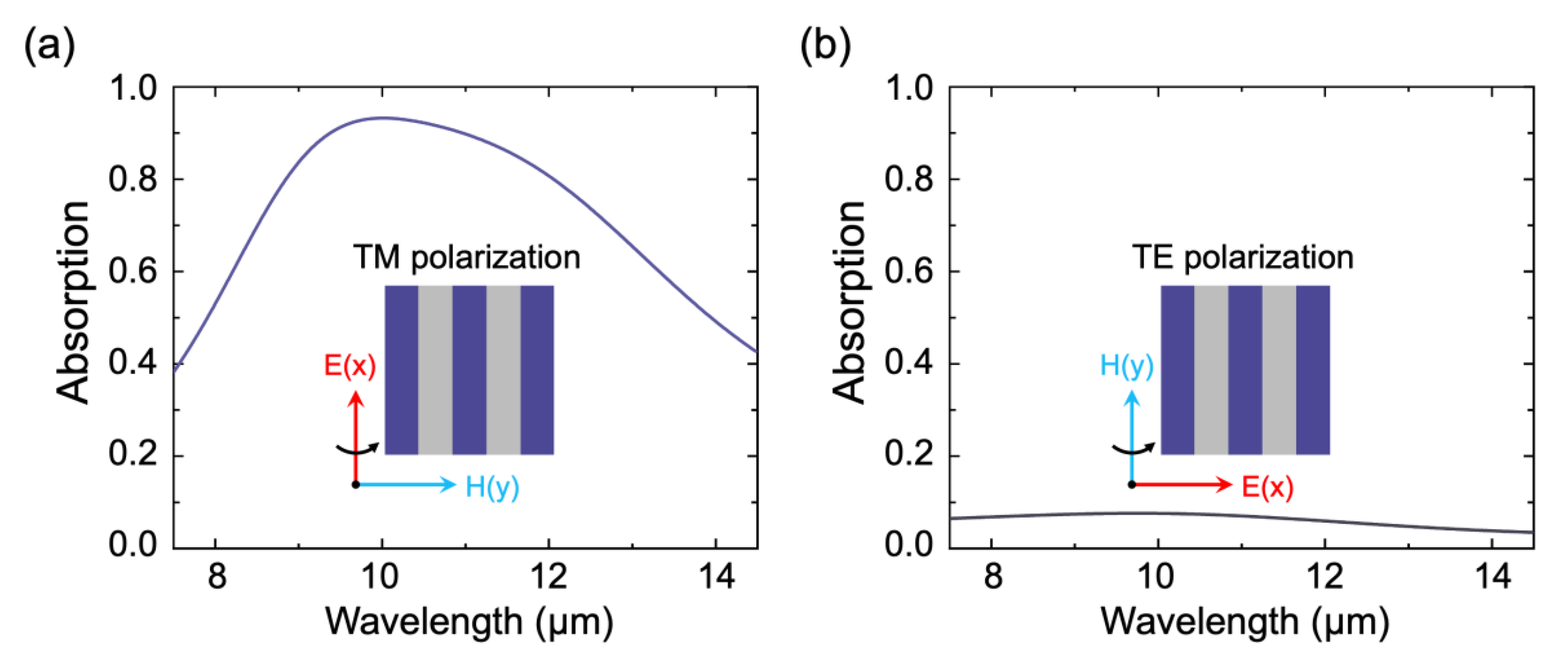
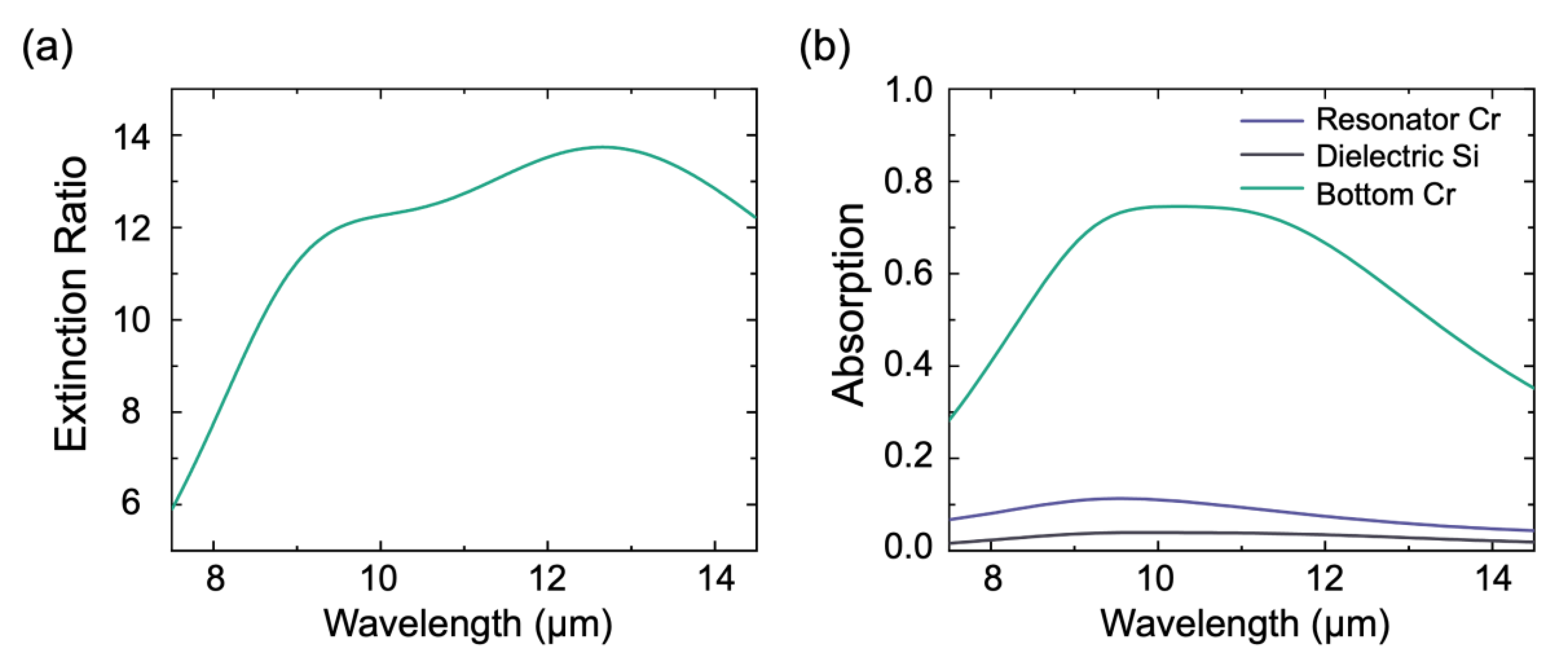
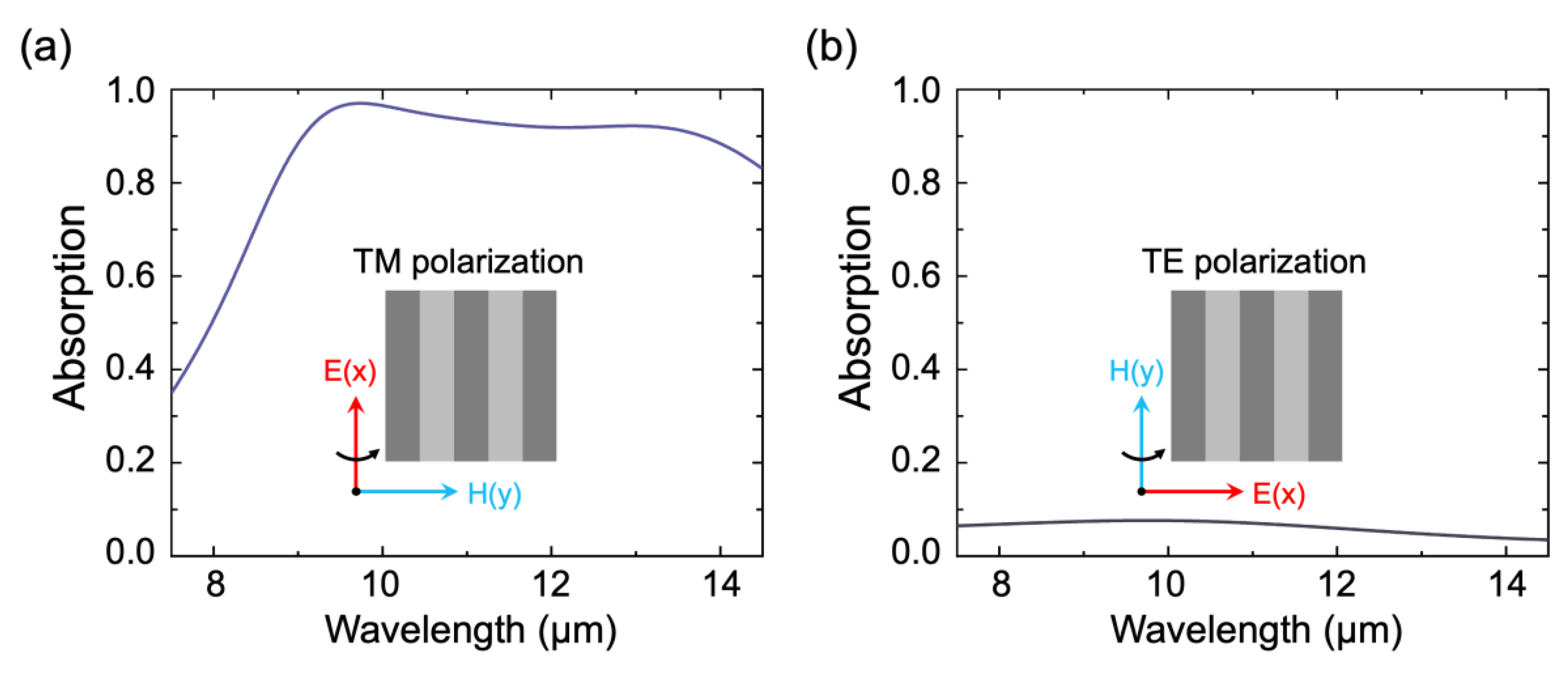
3. Results and Discussion

The absorption spectra of the absorber are shown in Figure 2a,b. Under TM-polarized light, the absorber has an absorption peak located at 10.0 µm, and the absorptance reaches 93.2%, as shown in Figure 2a by the purple solid line. In contrast to this, under TE-polarized light, there is almost no absorption in the entire LWIR atmospheric window.
The polarization extinction ratio, an index that directly describes polarization performance, is defined as [40]:
E R ( λ ) = A T M ( λ ) A T E ( λ )
where A T M ( λ ) and A T E ( λ ) are the absorptances under TM- and TE-polarized light, respectively. The corresponding polarization extinction ratio is shown in Figure 3a, and the average extinction ratio of the absorber reaches 11.92 in the LWIR atmospheric window.
To explain the physical mechanism of TM-polarized light absorption, we calculated the absorption of each layer in the microstructure, as shown in Figure 3b. The involved equation can be expressed as [41]:
Q ( ω ) = 1 2 × ω × Im ( ε ) × E 2 ( ω )
in which ω is the angular frequency, Im ( ε ) is the imaginary part of the dielectric permittivity, and E ( ω ) is the local electric field. Here, the electric field intensity used in the calculation is the relative value extracted from the simulation results below (see Figure 4a,b); thus, Q ( ω ) , as calculated by Equation (2), is not the actual value but instead the relative distribution. The results presented in Figure 3b illustrate that the absorption is mainly generated in the bottom layer (Cr). The absorption of Cr is induced by the excitation of PSPs at the interface of the metal plane bottom and the dielectric layer, and the absorption induced by LSPs is generated in both the grating resonators and metal plane bottom.
To further analyze this optical property, the electromagnetic field distribution at the absorption peak was numerically simulated. As shown in Figure 4a, we found that at 10.0 µm, the electric field is mainly concentrated on the edge of the metal grating resonators, which match the characteristics of the LSP. It can be judged that the absorption peak at 10.0 µm is caused by the enhancement of the localized electromagnetic field of the SPs. Specifically, under TM-polarized light, the LSPs of the grating structure are excited and then coupled to the dielectric layers and the metal plane bottom.
Next, as shown in Figure 4b, at 10.0 µm, the magnetic field is mainly distributed in the dielectric layer below the resonators, which can be attributed to the excitation of PSPs by the wave vector increment provided by the grating coupling and plasmonic resonant cavity. Specifically, the PSP is excited at the metal–dielectric interface and coupled through the resonant cavity to the metal plane bottom, which in turn changes the optical response and generates high absorption. This optical property can be expressed theoretically by the following equations [42]:
k = k 0 sin θ + i × 2 π p
k P S P = k 0 ε m ε d ε m + ε d
Equation (3) is the Bragg coupling condition, in which k 0 = ω C = 2 π λ is the free-space wave vector, θ is the angle of the incident electromagnetic wave, integer i is the diffraction order of the grating, and p is the grating period. Equation (4) indicates the wave vector of the PSPs; ε m and ε d are the dielectric constants of the metal and insulator medium, respectively. Only when k = k P S P does the incident electromagnetic wave couple to PSPs. In summary, the physical mechanism of the high absorption of TM-polarized light at 10.0 µm is attributed to the simultaneous excitation of PSPR and LSPR.
In contrast to narrowband absorbers, achieving a high-performance absorber with ultra-broadband high absorption is challenging. Numerous studies have been carried out to integrate multiple resonances horizontally or vertically into a single metamaterial cell to increase the intensity and bandwidth of absorption. Here, we present a unique approach to stacking dielectrics.
High-dispersion dielectrics such as silicon dioxide, silicon nitride, silicon carbide, and aluminum arsenide have intrinsic vibrational modes (optical phonons) in the infrared range [43,44]. We stacked a high-dispersion dielectric with a conventional dielectric and actively utilized the LSPs and PSPs excited by the resonance of the MIM absorber to couple them with the optical phonons of the dielectric, thus achieving a high-performance absorber with ultra-broadband and polarization selectivity.
We propose an absorber with a three-layer stack dielectric, Si3N4-Si-Si3N4, as shown in Figure 5. The total thickness of the absorber (772 nm) is still very thin, and the period of the absorber remains constant (800 nm). The corresponding structural parameters and numerical simulation results are shown in Table 1. The ultra-thin thickness and ultra-short cycle time help to improve the sensitivity of the detector.
The absorption spectra of the Cr-Si3N4-Si-Si3N4-Cr absorber are shown in Figure 6a-b. From the simulation results, under TM-polarized light, the absorber achieved a high absorption of 87.2% in a broadband wavelength range from 8 µm to 14 µm, covering the entire LWIR atmospheric window. Specifically, there is a 4750 nm bandwidth with an absorptance higher than 90%. As the solid purple line in Figure 6a shows, there are two absorption peaks in the simulated wavelength, located at 9.7 µm and 13.1 µm, respectively, and the corresponding absorptances reach 96.5% and 97.1%. Figure 7a shows the corresponding polarization extinction ratio of the proposed absorber, in which the absorber exhibits a high extinction ratio in a broadband wavelength range from 8 to 14 µm, and the average extinction ratio in the absorber reaches 13.50.
To better understand the absorption mechanism under TM-polarized light, we calculated the contribution of each layer in the structure to the incident light absorption by Equation (2), which is shown in Figure 7b, and numerically simulated the distribution of the electromagnetic field at absorption peaks, as shown in Figure 8a–d. We found that there is only a slight difference in the electromagnetic field distributions at p1 and p2. For a more accurate determination, we focused on the calculation results of the absorption of incident light by each layer of the structure. We found that the absorption is mainly generated in the bottom layer (Cr) and dielectric layer (Si3N4). Based on the results, we can conclude that the absorption in the bottom layer (Cr) is attributed to the simultaneous excitation of PSPR and LSPR, which is consistent with the first MIM absorber. In addition, the high absorption for the dielectric layer (Si3N4) originates from its own intrinsic vibrational modes (optical phonons), which coincides with our design. Specifically, the designed microstructure is composed of a high-dispersion dielectric with MIM absorbers, in which LSPs and PSPs excited by the resonance of the MIM absorber are coupled to the optical phonons of the dielectric, thereby modifying the optical response to further broaden the absorption band and improving the absorptance. This is why the proposed absorber exhibits ultra-broadband high-absorption behavior.
Finally, we evaluated the influence of the microstructure period tolerance on the absorption characteristics with respect to its manufacturing. With the development of microfabrication technologies, metamaterials can usually be fabricated by film deposition, photolithography, and ion-beam etching, among other techniques. Specifically, the multilayer structure of the proposed metamaterials can be prepared by magnetron sputtering or electron beam evaporation, while the upper grating array can be prepared by existing nanoprocessing methods, such as electron beam lithography (EBL) and nanoimprinting. These methods are capable of efficient mass production, but a considerable loss of absorber performance due to minor processing errors is inevitable. Here, the spectral stability of the designed absorber was evaluated, as shown in Figure 9. We analyzed the influence of geometric parameters on the performance of the proposed absorber. Whether the width of the grating changes (from 450 to 600 nm) or the period of the microstructure changes (from 700 to 1000 nm), the absorber possesses remarkably spectral stability. In this way, the loss of performance in manufacturing can be avoided to the maximum extent, signifying that our absorbers allow minor processing errors in fabrication and enable the performance to be stably maintained.
In order to further demonstrate the excellent performance of the metamaterial absorber designed in this paper, we performed a rough performance assessment, as shown in Figure 10. By comparison, our high-performance metamaterial absorber exhibits the following characteristics: (a) precise polarization-selective absorption in ultra-broadband, which can replace conventional polarizers to avoid the losses of the air gap between surface components and the detector so as to further simplify imaging systems; (b) ultra-thin thickness, which is ideal for directly integrating with detectors and is of great benefit in improving its performance in LWIR detection; and (c) remarkable spectral stability, which allows minor processing errors in manufacturing and enables the performance of the absorber to be maintained. Accordingly, the proposed absorber has great application potential in the future.

4. Conclusions

In summary, we successfully demonstrated a novel high-performance metamaterial absorber based on high-loss metals and high-dispersion dielectrics that exhibits ultra-broadband high absorption and polarization selectivity. In particular, as the excited LSPs and PSPs are coupled to optical phonons, the absorber generates an absorption bandwidth of 4750 nm in the LWIR atmospheric window with an absorption above 90%. In addition, the proposed absorber achieves remarkable spectral stability, which allows minor processing errors in fabrication and enables the performance to be maintained. The period of the metamaterial we designed is only 800 nm, which is significantly beneficial to improve the detection performance in terms of application but, inevitably, increases the requirement for processing accuracy in terms of fabrication. This is where we need to focus our efforts in the future: to explore more effective methods to achieve high-precision and low-cost manufacturing of metamaterials. In terms of potential practical applications, its precise polarization selectivity and ultra-thin thickness make the absorber ideal for integration with detectors. It can simplify imaging systems and improve detection performance simultaneously for gas detection, biosensors, and medical diagnostics.

Author Contributions

Conceptualization, Y.X.; methodology, Y.X.; software, Y.X.; formal analysis, Y.X.; investigation, Y.X. and J.Z.; resources, X.L., J.Z., X.W. (Xiaokun Wang), X.W. (Xiaoyi Wang), J.G. and H.Y.; writing—original draft preparation, Y.X.; writing—review and editing, X.L. and H.Y.; visualization, X.L.; supervision, X.L., X.W. (Xiaokun Wang), X.W. (Xiaoyi Wang), J.G. and H.Y.; project administration, X.L., X.W. (Xiaoyi Wang), J.G. and H.Y.; funding acquisition, J.G. and H.Y. All authors have read and agreed to the published version of the manuscript.

Funding

This work was supported by the National Natural Science Foundation of China (Nos. 61875193 and 62005272).

Institutional Review Board Statement

Not applicable.

Informed Consent Statement

Not applicable.

Data Availability Statement

The authors confirm that the data supporting the findings of this study are available within the article.

Conflicts of Interest

The authors declare no conflict of interest.

References

  1. Kildishev, A.V.; Boltasseva, A.; Shalaev, V.M. Planar Photonics with Metasurfaces. Science 2013, 339, 1289. [Google Scholar] [CrossRef] [PubMed]
  2. Hu, Y.; Wang, X.; Luo, X.; Ou, X.; Li, L.; Chen, Y.; Yang, P.; Wang, S.; Duan, H. All-dielectric metasurfaces for polarization manipulation: Principles and emerging applications. Nanophotonics 2020, 9, 3755–3780. [Google Scholar] [CrossRef]
  3. Cerjan, B.; Gerislioglu, B.; Link, S.; Nordlander, P.; Halas, N.J.; Griep, M.H. Towards scalable plasmonic Fano-resonant metasurfaces for colorimetric sensing. Nanotechnology 2022, 33, 405201. [Google Scholar] [CrossRef] [PubMed]
  4. Chu, Y.; Banaee, M.G.; Crozier, K.B. Double-Resonance Plasmon Substrates for Surface-Enhanced Raman Scattering with Enhancement at Excitation and Stokes Frequencies. ACS Nano 2010, 4, 2804–2810. [Google Scholar] [CrossRef] [PubMed]
  5. Smith, D.R.; Padilla, W.J.; Vier, D.C.; Nemat-Nasser, S.C.; Schultz, S. Composite Medium with Simultaneously Negative Permeability and Permittivity. Phys. Rev. Lett. 2000, 84, 4184–4187. [Google Scholar] [CrossRef] [PubMed]
  6. Shelby, R.A.; Smith, D.R.; Schultz, S. Experimental Verification of a Negative Index of Refraction. Science 2001, 292, 77–79. [Google Scholar] [CrossRef]
  7. Yu, N.; Aieta, F.; Genevet, P.; Kats, M.A.; Gaburro, Z.; Capasso, F. A broadband, background-free quarter-wave plate based on plasmonic metasurfaces. Nano Lett. 2012, 12, 6328–6333. [Google Scholar] [CrossRef]
  8. Fa Ng, N.; Lee, H.; Cheng, S.; Zhang, X. Sub-Diffraction-Limited Optical Imaging with a Silver Superlens. Science 2005, 308, 534–537. [Google Scholar] [CrossRef]
  9. Khorasaninejad, M.; Chen, W.T.; Devlin, R.C.; Oh, J.; Zhu, A.Y.; Capasso, F. Metalenses at visible wavelengths: Diffraction-limited focusing and subwavelength resolution imaging. Science 2016, 352, 1190–1194. [Google Scholar] [CrossRef]
  10. Lin, H.; Xu, Z.Q.; Cao, G.; Zhang, Y.; Jia, B. Diffraction-limited imaging with monolayer 2D material-based ultrathin flat lenses. Light Sci. Appl. 2020, 9, 137. [Google Scholar] [CrossRef]
  11. Huang, X.; Lai, Y.; Hang, Z.H.; Zheng, H.; Chan, C.T. Dirac cones induced by accidental degeneracy in photonic crystals and zero-refractive-index materials. Nat. Mater. 2011, 10, 582–586. [Google Scholar] [CrossRef] [PubMed]
  12. Xu, H.X.; Hu, G.; Wang, Y.; Wang, C.; Wang, M.; Wang, S.; Huang, Y.; Genevet, P.; Huang, W.; Qiu, C.W. Polarization-insensitive 3D conformal-skin metasurface cloak. Light Sci. Appl. 2021, 10, 75. [Google Scholar] [CrossRef] [PubMed]
  13. Zheng, G.; Mühlenbernd, H.; Kenney, M.; Li, G.; Zentgraf, T.; Zhang, S. Metasurface holograms reaching 80% efficiency. Nat. Nanotechnol. 2015, 10, 308–312. [Google Scholar] [CrossRef]
  14. Guo, X.; Zhong, J.; Li, B.; Qi, S.; Li, Y.; Li, P.; Wen, D.; Liu, S.; Wei, B.; Zhao, J. Full-Color Holographic Display and Encryption with Full-Polarization Degree of Freedom. Adv. Mater. 2022, 34, 2103192. [Google Scholar] [CrossRef]
  15. Tao, J.; You, Q.; Li, Z.L.; Luo, M.; Liu, Z.C.; Qiu, Y.; Yang, Y.; Zeng, Y.Q.; He, Z.X.; Xiao, X.; et al. Mass-Manufactured Beam-Steering Metasurfaces for High-Speed Full-Duplex Optical Wireless-Broadcasting Communications. Adv. Mater. 2022, 34, 2106080. [Google Scholar] [CrossRef] [PubMed]
  16. Kim, S.J.; Fan, P.; Kang, J.H.; Brongersma, M.L. Creating semiconductor metafilms with designer absorption spectra. Nat. Commun. 2015, 6, 7591. [Google Scholar] [CrossRef]
  17. Xie, Y.Y.; Ni, P.N.; Wang, Q.H.; Kan, Q.; Briere, G.; Chen, P.P.; Zhao, Z.Z.; Delga, A.; Ren, H.R.; Chen, H.D. Metasurface-integrated vertical cavity surface-emitting lasers for programmable directional lasing emissions. Nat. Nanotechnol. 2020, 15, 125–130. [Google Scholar] [CrossRef]
  18. Iyer, P.P.; Decrescent, R.A.; Mohtashami, Y.; Lheureux, G.; Schuller, J.A. Unidirectional luminescence from InGaN/GaN quantum-well metasurfaces. Nat. Photonics 2020, 14, 1–6. [Google Scholar] [CrossRef]
  19. Landy, N.I.; Sajuyigbe, S.; Mock, J.J.; Smith, D.R.; Padilla, W.J. Perfect metamaterial absorber. Phys. Rev. Lett. 2008, 100, 207402. [Google Scholar] [CrossRef]
  20. Liu, N.; Mesch, M.; Weiss, T.; Hentschel, M.; Giessen, H. Infrared perfect absorber and its application as plasmonic sensor. Nano Lett. 2010, 10, 2342–2348. [Google Scholar] [CrossRef]
  21. Li, W.; Valentine, J. Metamaterial perfect absorber based hot electron photodetection. Nano Lett. 2014, 14, 3510–3514. [Google Scholar] [CrossRef] [PubMed]
  22. Shahsafi, A.; Joe, G.; Brandt, S.; Shneidman, A.V.; Stanisic, N.; Xiao, Y.; Wambold, R.; Yu, Z.; Salman, J.; Aizenberg, J.; et al. Wide-Angle Spectrally Selective Absorbers and Thermal Emitters Based on Inverse Opals. ACS Photonics 2019, 6, 2607–2611. [Google Scholar] [CrossRef]
  23. Tittl, A.; Michel, A.K.; Schaferling, M.; Yin, X.; Gholipour, B.; Cui, L.; Wuttig, M.; Taubner, T.; Neubrech, F.; Giessen, H. A Switchable Mid-Infrared Plasmonic Perfect Absorber with Multispectral Thermal Imaging Capability. Adv. Mater. 2015, 27, 4597–4603. [Google Scholar] [CrossRef] [PubMed]
  24. Zeng, B.; Huang, Z.; Singh, A.; Yao, Y.; Azad, A.K.; Mohite, A.D.; Taylor, A.J.; Smith, D.R.; Chen, H.T. Hybrid graphene metasurfaces for high-speed mid-infrared light modulation and single-pixel imaging. Light Sci. Appl. 2018, 7, 51. [Google Scholar] [CrossRef]
  25. Liu, X.; Trosseille, J.; Mongruel, A.; Marty, F.; Basset, P.; Laurent, J.; Royon, L.; Cui, T.; Beysens, D.; Bourouina, T. Tailoring silicon for dew water harvesting panels. IScience 2021, 24, 102814. [Google Scholar] [CrossRef]
  26. Aydin, K.; Ferry, V.E.; Briggs, R.M.; Atwater, H.A. Broadband polarization-independent resonant light absorption using ultrathin plasmonic super absorbers. Nat. Commun. 2011, 2, 517. [Google Scholar] [CrossRef]
  27. Liu, X.; Gao, J.; Gao, J.; Yang, H.; Wang, X.; Wang, T.; Shen, Z.; Zhen, L.; Liu, H.; Zhang, J. Microcavity electrodynamics of hybrid surface plasmon polariton modes in high-quality multilayer trench gratings. Light Sci. Appl. 2018, 7, 14. [Google Scholar] [CrossRef]
  28. Dixon, K.; Montazeri, A.O.; Shayegannia, M.; Barnard, E.S.; Cabrini, S.; Matsuura, N.; Holman, H.Y.; Kherani, N.P. Tunable rainbow light trapping in ultrathin resonator arrays. Light Sci. Appl. 2020, 9, 194. [Google Scholar] [CrossRef]
  29. Liu, X.; Gao, J.; Wang, Y.; Wang, X.; Yang, H.; Hu, H.; Gao, J.; Bourouina, T.; Cui, T. Simultaneous field enhancement and loss inhibition based on surface plasmon polariton mode hybridization. Nanophotonics 2020, 9, 2809–2816. [Google Scholar] [CrossRef]
  30. Su, Y.-H.; Ke, Y.-F.; Cai, S.-L.; Yao, Q.-Y. Surface plasmon resonance of layer-by-layer gold nanoparticles induced photoelectric current in environmentally-friendly plasmon-sensitized solar cell. Light Sci. Appl. 2012, 1, e14. [Google Scholar] [CrossRef]
  31. Lin, K.-T.; Chen, H.-L.; Lai, Y.-S.; Yu, C.-C. Silicon-based broadband antenna for high responsivity and polarization-insensitive photodetection at telecommunication wavelengths. Nat. Commun. 2014, 5, 3288. [Google Scholar] [CrossRef] [PubMed]
  32. Li, Q.; Li, Z.; Wang, X.; Wang, T.; Liu, H.; Yang, H.; Gong, Y.; Gao, J. Structurally tunable plasmonic absorption bands in a self-assembled nano-hole array. Nanoscale 2018, 10, 19117–19124. [Google Scholar] [CrossRef] [PubMed]
  33. He, C.; He, H.; Chang, J.; Chen, B.; Ma, H.; Booth, M.J. Polarisation optics for biomedical and clinical applications: A review. Light Sci. Appl. 2021, 10, 194. [Google Scholar] [CrossRef] [PubMed]
  34. Zhang, L.; Zheng, Y.; Zhang, J.; Yin, Y.; Li, Q.; Lei, J.; Zhu, Y. Tunable polarization-sensitive, long-wave infrared MDM subwavelength grating structure with wide-angle, narrow-band, and high absorption. Opt. Express 2021, 29, 21473–21491. [Google Scholar] [CrossRef] [PubMed]
  35. Hwang, J.; Ku, Z.; Jeon, J.; Kim, Y.; Kim, D.-K.; Kim, E.K.; Lee, S.J. Polarization-Sensitive and Wide Incidence Angle-Insensitive Fabry–Perot Optical Cavity Bounded by Two Metal Grating Layers. Sensors 2020, 20, 5382. [Google Scholar] [CrossRef]
  36. Gong, Y.; Wang, Z.; Li, K.; Uggalla, L.; Huang, J.; Copner, N.; Zhou, Y.; Qiao, D.; Zhu, J. Highly efficient and broadband mid-infrared metamaterial thermal emitter for optical gas sensing. Opt. Lett. 2017, 42, 4537–4540. [Google Scholar] [CrossRef]
  37. Li, J.; Gan, R.; Guo, Q.; Liu, H.; Xu, J.; Yi, F. Tailoring optical responses of infrared plasmonic metamaterial absorbers by optical phonons. Opt. Express 2018, 26, 16769–16781. [Google Scholar] [CrossRef]
  38. Wang, W.; Qu, Y.; Du, K.; Bai, S.; Tian, J.; Pan, M.; Ye, H.; Qiu, M.; Li, Q. Broadband optical absorption based on single-sized metal-dielectric-metal plasmonic nanostructures with high-ε″ metals. Appl. Phys. Lett. 2017, 110, 101101. [Google Scholar] [CrossRef]
  39. Palik, E.D. Handbook of Optical Constants of Solids II; Academic Press: Cambridge, MA, USA, 1985. [Google Scholar]
  40. Presnar, M.D.; Raisanen, A.D.; Pogorzala, D.R.; Kerekes, J.P.; Rice, A.C. Dynamic Scene Generation, Multimodal Sensor Design, and Target Tracking Demonstration for Hyperspectral/Polarimetric Performance-Driven Sensing. In Proceedings of the SPIE—The International Society for Optical Engineering, Orlando, FL, USA, 26 April 2010; Volume 7672, pp. 218–229. [Google Scholar]
  41. Ferry, V.E.; Sweatlock, L.A.; Pacifici, D.; Atwater, H.A. Plasmonic Nanostructure Design for Efficient Light Coupling into Solar Cells. Nano Lett. 2008, 8, 4391–4397. [Google Scholar] [CrossRef]
  42. Barnes, W.L. Surface plasmon–polariton length scales: A route to sub-wavelength optics. J. Opt. A Pure Appl. Opt. 2006, 8, S87. [Google Scholar] [CrossRef]
  43. Üstün, K.; Turhan-Sayan, G. Wideband long wave infrared metamaterial absorbers based on silicon nitride. J. Appl. Phys. 2016, 120, 203101. [Google Scholar] [CrossRef]
  44. Guo, Q.; Guinea, F.; Deng, B.; Sarpkaya, I.; Li, C.; Chen, C.; Ling, X.; Kong, J.; Xia, F. Electrothermal Control of Graphene Plasmon–Phonon Polaritons. Adv. Mater. 2017, 29, 1700561–1700566. [Google Scholar] [CrossRef] [PubMed]
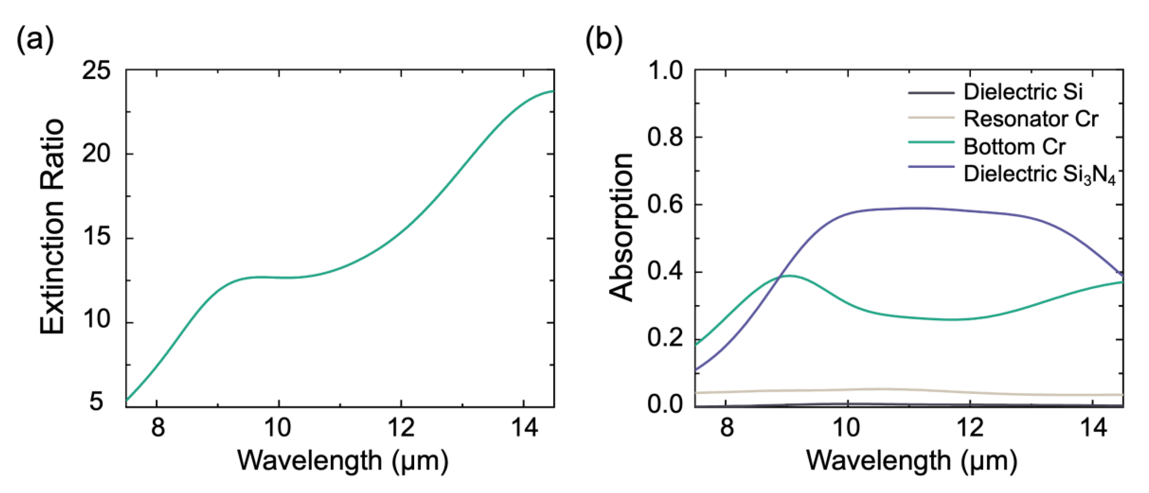
Figure 1. Diagram of metal-insulator-metal (MIM) absorber with p = 800 nm, w = 560 nm, h = 200 nm, d = 400 nm, and t = 22 nm. (a) Three-dimensional schematic of the absorber and (b) cross-section of the absorber along the x-y plane.
Coatings 12 01194 g001
Figure 2. Simulated absorption spectrum of designed MIM absorber under (a) TM- and (b) TE-polarized light.
Coatings 12 01194 g002
Figure 3. (a) Polarization extinction ratio of designed MIM absorber; (b) absorbed energy distribution within each component of absorber structures.
Coatings 12 01194 g003
Figure 4. (a) Electric field distribution at absorption peak at 10.0 µm under TM-polarized light; (b) magnetic field distribution at absorption peak at 10.0 µm under TM-polarized light.
Coatings 12 01194 g004
Figure 5. Diagram of high-performance metamaterial absorber with p = 800 nm, w = 560 nm, h = 200 nm, d = 550 nm, and t = 22 nm.
Coatings 12 01194 g005
Figure 6. Simulated absorption spectrum of designed high-performance metamaterial absorber under (a) TM- and (b) TE-polarized light.
Coatings 12 01194 g006
Figure 7. (a) Polarization extinction ratio of designed absorber; (b) absorbed energy distribution within each component of absorber structures.
Coatings 12 01194 g007
Figure 8. (a) Electric field and (b) magnetic field distribution at absorption peak at 9.7µm under TM-polarized light; (c) electric field and (d) magnetic field distribution at absorption peak at 13.1 under TM-polarized light.
Coatings 12 01194 g008
Figure 9. Simulated absorption behavior for absorber as a function of (a) width of the wire grating and (b) period of the microstructure: as the geometric parameters change, the position of the absorption spectrum is almost insensitive.
Coatings 12 01194 g009
Figure 10. Performance assessment of the MIM absorber and high-performance absorber compared with a conventional absorber.
Coatings 12 01194 g010
Table 1. Comparison of structural parameters and numerical simulation results of designed metamaterials.
MetasurfaceMaterialThicknessSpacer CompositionAbsorption BandwidthAverage AbsorptionMaximum Extinction Ratio
S1Cr
Si
622 nm400 nm Si1580 nm78.2%13.74
S2Cr
Si
Si3N4
772 nm20 nm Si3N4
200 nm Si
330 nm Si3N4
4750 nm87.2%23.72
Publisher’s Note: MDPI stays neutral with regard to jurisdictional claims in published maps and institutional affiliations.

