Article

Fundamental Properties of Transition-Metals-Adsorbed Germanene: A DFT Study

1
Department of Physics/QTC/Hi-GEM, National Cheng Kung University, Tainan 70148, Taiwan
2
Center of General Studies, National Kaohsiung University of Science and Technology, Kaohsiung 811213, Taiwan
3
Department of Energy and Refrigerating Air-Conditioning Engineering, National Kaohsiung University of Science and Technology, Kaohsiung 811213, Taiwan
*
Author to whom correspondence should be addressed.
Coatings 2022, 12(7), 948; https://doi.org/10.3390/coatings12070948
Submission received: 13 May 2022 / Revised: 12 June 2022 / Accepted: 1 July 2022 / Published: 4 July 2022
(This article belongs to the Special Issue 2D Materials-Based Thin Films and Coatings)

Abstract

:
The transition metal (TM)-absorbed germanene systems enriched by strong chemical bonding are investigated using first-principles calculations. Dedicated calculations include the geometry, preferable adsorption sites, atom-dominated band structure, spin–density distributions, spatial charge distribution, and the projected density of states (DOS). The strong multi-orbital chemical bonds between TMs and Ge atoms can create seriously buckled structures and a non-uniform chemical environment, which are responsible for the unusual electronic properties. Of the three chosen systems, the Fe–Ge and Co–Ge ones possess magnetic properties, while the Ni–Ge system exhibits non-magnetic behavior. The orbital-hybridization-induced characteristics are revealed in van Hove singularities of the DOS.

1. Introduction

Following the initial discovery of graphene by mechanical exfoliation of a graphite surface, other group-IV two-dimensional (2D) honeycomb lattice systems such as silicene, germanene, and stanene have attracted considerable attention in theory [1,2,3,4,5] and experiments [6,7,8,9]. It is known that C, Si, Ge, Sn, and Pb belong to the same group IV in the periodic table that can generate the σ , π , and s p 3 chemical bonds because they possess (2s, 2 p x , 2 p y , 2 p z ), (3s, 3 p x , 3 p y , 3 p z ), (4s, 4 p x , 4 p y , 4 p z ), (5s, 5 p x , 5 p y , 5 p z ), and (6s, 6 p x , 6 p y , 6 p z ) orbitals, respectively. Similar to graphene, germanene and silicene have many exceptional properties, such as high carrier mobility and ultrafast optical absorption spectra [10,11], because of their hexagonal honeycomb lattices and Dirac-cone electronic band structure. However, based on the calculations of density functional theory (DFT) for structure optimization, phonon dispersion, and ab initio finite temperature molecular dynamics, the planar honeycomb structure of monolayer silicene/germanene is its least energetic configuration and is not stable (this may be attributed to the larger atomic radius of Si/Ge than that of C), whereas the low-buckled silicene/germanene are thermally stable [12]. The low-buckled honeycomb structure creates s p 2 - s p 3 hybridization rather than pure s p 2 hybridization as in graphene. The greatly enhanced intrinsic spin–orbit coupling causes many important features to be more prominent in germanene than in graphene, e.g., the easily tunable bandgap, quantum anomalous spin Hall effect, and strong valley polarization [13,14,15]. These outstanding features make germanene and silicene potential candidates for a wide range of applications, including field-effect transistors, batteries, sensors, infrared optics, and spintronic/valleytronic devices.
Although germanene has not been found in nature, it can be synthesized by a few methods, such as molecular beam epitaxial (MBE) [16] and topological deintercalation [17]. The production of germanene by the MBE method on different substrates has been reported in several previous studies, but this method still has several drawbacks, including limited extensible space, vertical scale heterogeneity, and the difficulty in transferring synthesized materials from the substrate to a free-standing form. On the other hand, topochemical deintercalation is an effective method for producing 2D silicene and germanene in a free-standing form, thereby overcoming the disadvantages of the MBE method. The successful synthesis of 2D buckled germanene in free-standing form is extremely important because this approach can avoid the interactions with the substrate that could cause unexpected effects. This makes it easier to incorporate germanene into practical products or produce functionalized germanene for possible applications.
In general, the electronic, magnetic, and optical properties of a material can be modified by several techniques, such as chemical adatom adsorption/substitution, introduction of defects/vacancies, and formation of heterojunctions, as well as by applying the gate voltages, magnetic fields, and mechanical strain. Among these, chemical modifications including adsorptions and substitutions are especially effective strategies when applied to 2D materials, because these materials possess a more active surface environment [18,19].
In this work, we investigate Fe-/Co-/Ni-adsorbed germanenes. It is known that TM-adsorbed/doped systems have extensive applications in catalysis, nonlinear optical response, etc. [20,21,22]. Such systems possess a non-uniform chemical environment that enriches the chemical bonds and electric properties, such as the metal/semiconductor behavior and the ferromagnetic, antiferromagnetic, or non-magnetic properties, depending on the type and position of the guest atom. Here, we focus on how a non-uniform chemical environment enriches chemical bonds and electrical properties, which was not explored in depth in previous studies [23,24,25]. To enhance the effects, a higher concentration of TM adatoms is considered (TM:Ge = 1:6). The results are quite different from the results obtained at a relatively lower concentration, e.g., TM:Ge = 1:32 [26,27]. For example, at a lower TM concentration, the low-energy bands of Fe-, Co-, and Ni-Ge systems present a pair of gapped linear bands around the high-symmetric K point, which are contributed by the Ge atoms. Therefore, the systems are metal or direct-gap semiconductors. Such low-lying linear bands are totally absent under a higher TM concentration. Instead, there exist many low-lying oscillating parabolic subbands, which are dominated by the adatoms near E F = 0 and co-dominated by TM and Ge atoms at higher/lower energies. These oscillating parabolic subbands, arising from the more seriously buckled structure and the stronger multi-orbital chemical bonds between the TM and Ge atoms, lead to metal or indirect-gap semiconducting behaviors. The band structures presented in this work display the atom contributions and the spin up/down states simultaneously, which make the unusual energy dispersions easy to understand. Furthermore, the charge density distribution reveals the asymmetrical charge accumulation of the TM-Ge bonds, indicating a non-uniform chemical environment. Most importantly, we present a delicate atom-, orbital-, and spin-decomposed DOS that shows the complete Ge (4s, 4 p x , 4 p y , 4 p z ) and TM (4s, 3 d x y , 3 d y z , 3 d x , 3 d z 2 , 3 d x 2 y 2 ) orbitals; no other papers have presented this detail. We demonstrate that the four/six orbitals of the host and guest atoms may overlap at certain energies, illustrating the multi-orbital hybridizations in any chemical bond. The theoretical framework built from the first-principles simulations is used to understand the significance of chemical bonds in generating rich and unique geometrical structures as well as custom-tailored electronic and magnetic properties. The theoretical predictions about the geometrical structures, band structures, van Hove singularities, and charge/spin–density distributions can be verified through high-resolution scanning tunneling microscopy/transmission electron microscopy (HRSTM/TEM) [28,29], angle-resolved photoemission spectroscopy (ARPES) [30], scanning tunneling spectroscopy (STS) [31], and STM spin excitation spectroscopy [32], respectively.

2. Materials and Methods

The first-principles calculations are based on density functional theory (DFT) [33,34] implemented by the Vienna ab initio simulation package (VASP) [35,36]. The Perdew–Burke–Ernzerhof (PBE) generalized gradient approximation method (GGA) [37] was employed to evaluate the electron–electron Coulomb interactions, while the electron–ion interactions were treated by the projector augmented-wave method [38]. The spin configurations were taken into account to meticulously explore the effects of chemical adsorption on the magnetic properties. The 2D periodic boundary conditions were along the x and y-axes. To avoid the interaction between adjacent unit cells, a vacuum distance along the z-axis was set to 15 Å. The cut-off energies of the wave function expanded by plane waves were chosen to be 500 eV for all calculations. The pristine first Brillouin zone was sampled by 9 × 9 × 1 and 100 × 100 × 1 k-points, respectively, for the geometry optimization and for further evaluations of the electronic and magnetic properties within the Gamma scheme. During the relaxation process, the Hellmann–Feynman force convergence on each atom was set to be 0.01 eV/Å, and the difference of eigenvalues between two simulation steps was less than 10 5 eV. Each system is in its most stable spin state.

3. Results

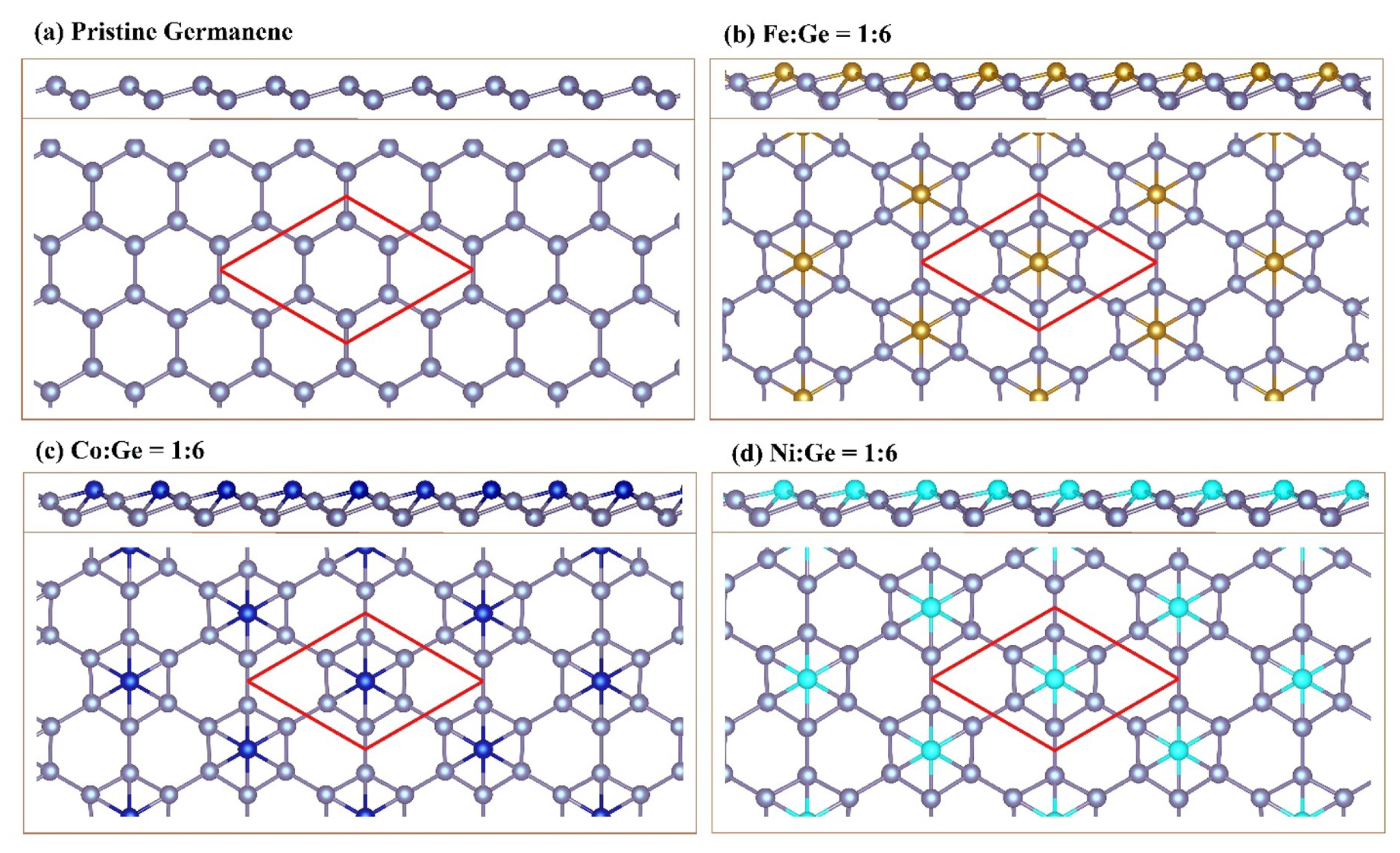
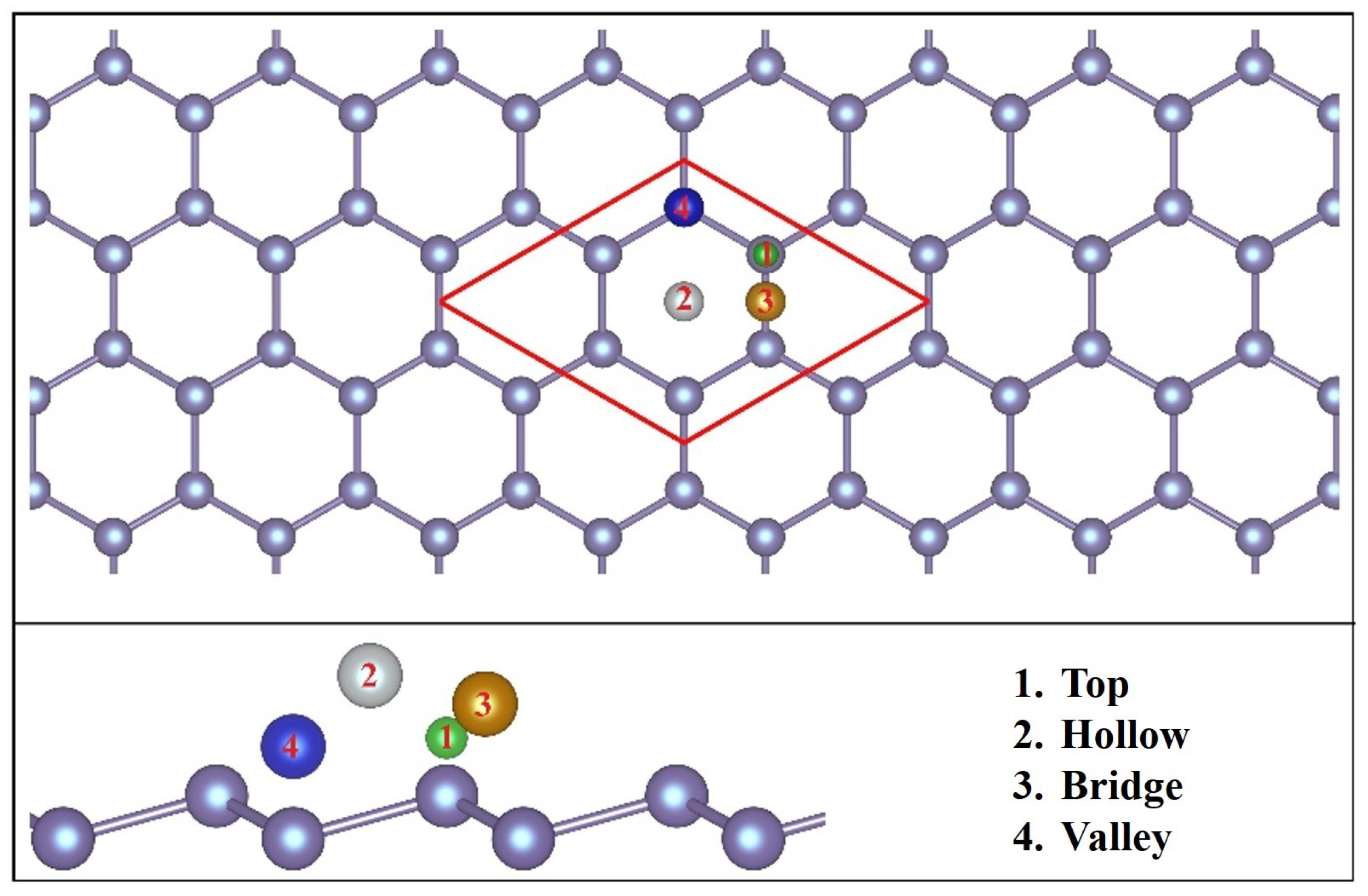
3.1. Geometric Structures
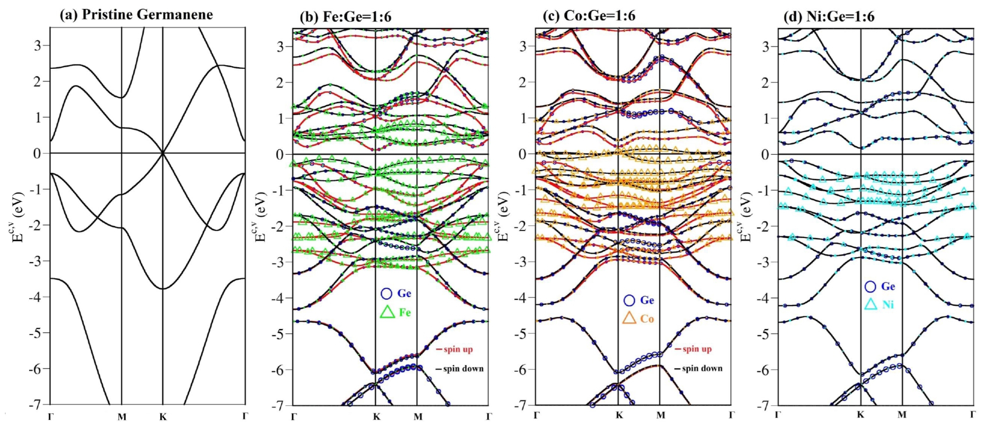
The TM-adsorbed germanene systems were modeled by a 3 × 3 germanene supercell, corresponding to TM:Ge = 1:6, as shown in Figure 1. Figure 2 shows the four possible adsorption sites usually considered in a buckled honeycomb lattice structure [39,40]; they are the top site (on the top of the upper Ge atom), the valley site (on the top of the lower Ge atom), the hollow site (above the center of the honeycomb structure), and the bridge site (on the top of the middle Ge–Ge bond). However, it has been found that if the TM atoms are placed on the bridge site, they always move to the valley position after structural relaxations. Therefore, bridge site adsorption is not achievable in a germanene system. The absorption energy is calculated by E a d s = E T M + E G e E ( G e + T M ) , where E T M , E G e , and E ( G e + T M ) are the total energies of an isolated TM atom, the germanene supercell, and the TM-adsorbed germanene system, respectively. A larger E a d s implies that the site is more favorable for the absorption of the TM on the germanene. Table 1 shows the E a d s of the valley, hollow, and top sites. Obviously, the hollow site is the most favorite site for all three TMs, while the valley site is the second-most-preferable one for Fe, and the top site is the second-most-favorable for Co and Ni. In general, the adsorption energies of the TM-adsorbed germanene systems are larger than those in TM-adsorbed graphene and silicene [39]. This suggests that germanene might be the better candidate to accommodate TM atoms.
The geometrical parameters of TM adatoms on the hollow site (the most energetically favorable) are shown in Table 1. These include the adatom heights over the germanene surface (h), the bond lengths between the adatom and its neighboring Ge atoms (X–Ge) and between two Ge atoms (Ge–Ge), and the buckling heights of the adsorption systems. In general, the Ge–Ge bond lengths and the buckling heights are increased compared to pristine germanene. The adatom height h reveals that among the three TMs, the Ni adatom is the nearest to the germanene surface, leading to the largest buckling (1.35 Å). Because of the buckling structure, there are two values of X–Ge bond length for each adatom. Among the three TMs, Co has the longest X–Ge bond length, while Fe has the longest Ge–Ge bond length. The latter possesses the largest magnetic moment ( μ = 2.73 μ B ). Obviously, the presence of TM atoms causes significant lattice distortions and creates highly asymmetric chemical environments, as shown by the TM–Ge/Ge–Ge bond lengths and the increased buckling. The highly asymmetric chemical environments are expected to generate complicated charge distributions and enrich the electronic properties.

3.2. Energy Bands

The band structures of pristine germanene and the three TM-adsorbed (on hollow sites) germanene systems are presented in Figure 3. In pristine monolayer germanene (Figure 3a), the band structures are characterized by π , σ , and s p 3 bonds. The system exhibits a modified Dirac cone structure at the K point. At low energies, the valence and conduction bands are generally symmetric about E F = 0 with a narrow gap of about 23.9 meV caused by the spin–orbit coupling. The π / π * band generated by the 4 p z orbital is initiated at the Γ M valley and displays a saddle M-point at −1.15/0.7 eV. On the other hand, the σ band, mainly created by ( 4 p x , 4 p y ) orbitals, exhibits a parabolic energy dispersion beginning at −0.6 eV at the Γ point and shows a saddle M-point at −2 eV. An observable mixing of π and σ bands in both the Γ M and Γ K paths demonstrates a weak but significant s p 3 bonding (nonorthogonality of π and σ bonds). It is noted that the coordinates of the high-symmetry points in the Brillouin zone are expressed by the linear combinations of the reciprocal lattice vectors: k = x 1 b 1 + x 2 b 2 + x 3 b 3 ; therefore, Γ = ( 0 , 0 ) , M = ( 0.5 , 0 ) , and K = ( 0.67 , 0.33 ) .
Compared with the pristine germanene, the Fe-adsorbed system presents an unusual electronic band dispersion, as shown in Figure 3b. The low-lying energy bands are mainly contributed by the greatly distorted π bonding on the germanene surface. The original Dirac cone is completely destroyed along with the highly asymmetric conduction and valence bands against E F = 0 . The lowest unoccupied states are located at the K point, while the highest occupied states are located between the Γ and M points. Therefore, the system is an indirect-gap semiconductor with E g = 0.22 (GGA could underestimate the bandgap due to the limitations of Kohn–Sham DFT [41]). Apparently, these novel features result from the complicated multi-orbital hybridizations of the non-uniform chemical bonds. It is noteworthy that Fe-adsorbed germanene exhibits a ferromagnetic configuration that is characterized by the two spin-split valence and conduction subbands near E F = 0 . These subbands exhibit non-monotonic wave-vector dependencies that might be closely related to the different contributions of the guest adatom and host atoms. In general, the subbands around E F = 0 are mainly dominated by the Fe atoms, and those at higher/lower energies are co-dominated by Fe and Ge atoms.
Similar spin-split energy subbands are also observed in Co-adsorbed germanene, as shown in Figure 3c. However, these subbands cross the Fermi level and create numerous valence holes/conduction electrons. The system exhibits metallic behavior, and the Dirac cone structure is totally absent. This indicates that the original π bond in pristine germanene has undergone a drastic transformation. The Co atoms (orange triangles) completely dominate the subbands near E F = 0 , while Ge atoms (blue circles) contribute to the lower subbands. There are several weakly oscillating and partially flat subbands in the region of −1 eV < E v < 0 eV. These subbands will cause prominent structures in the van Hove singularities in the density of states (DOS) (discussed in Figure 6).
The Ni-adsorbed germanene is an indirect-gap semiconductor with E g = 0.36 eV, as shown in Figure 3d. The asymmetry between valence and conduction bands about E F = 0 is extremely enhanced after Ni adsorption. The lowest unoccupied states are located at the K valley, while the highest occupied states are located in the K Γ path. The Ni-adsorbed germanene system is a non-magnetic material regardless of the position of the adsorbed adatom. In short, TM-absorbed germanene can create a non-uniform chemical environment with complex chemical bonds and unique band structures. It is difficult to distinguish the initial, middle (saddle-point structures), and final π and σ bands. Therefore, these results could not be well described by using a tight-binding model with complex multi-orbital hopping integrals, site energies, and the Hubbard-like spin-induced on-site Coulomb interactions [42].

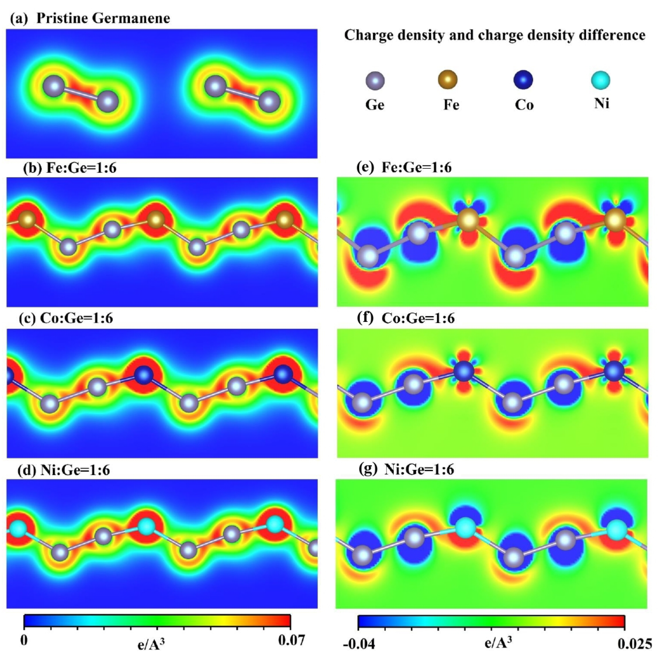
3.3. Spatial Charge Density Distribution
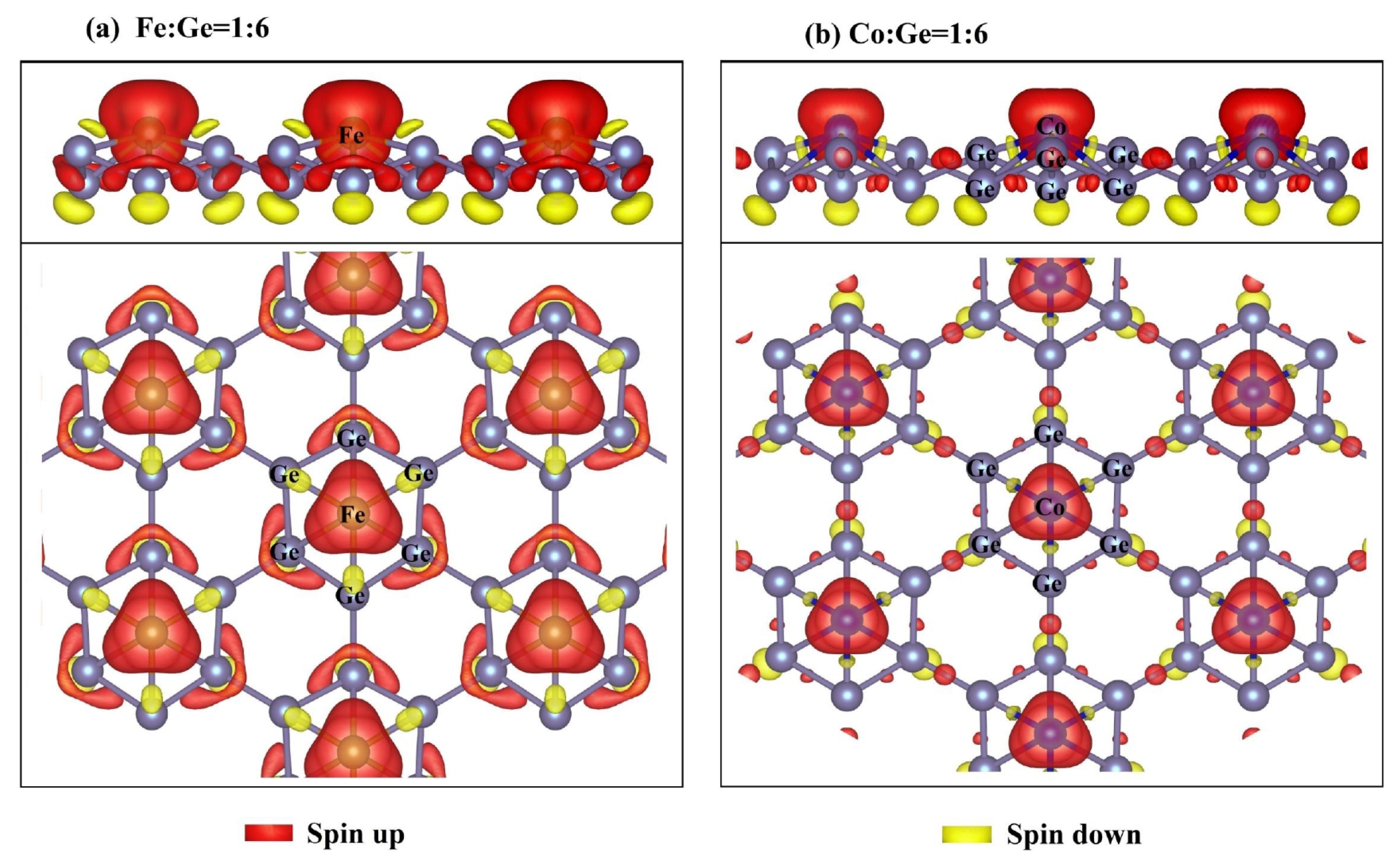
The charge density distribution ( ρ ) (the left panels of Figure 4) is closely related to the electron orbitals of each atom and is very sensitive to the distance between nearest neighbor atoms. It can provide very useful information about multi-/single-orbital hybridizations due to various chemical bonds and charge transfer phenomena between atoms. The three absorption cases show that the charges are concentrated around the TM atoms (the red areas in Figure 4b–d), indicating the asymmetrical charge accumulation of the TM–Ge bonds. On the other hand, the bond strength between Ge–Ge atoms is decreased in the presence of TM atoms, as reflected by the reduced red area compared to that of pristine germanene (Figure 4a). The distinct bond lengths/strengths and the charge density distributions between TM–Ge and Ge–Ge atoms demonstrate the highly non-uniform chemical environment that can be classified into light-green, yellow/light red, and red regions, which mainly correspond to 4 p z , (4s, 4 p x , 4 p y ), and (3 d x 2 y 2 , 3 d x y , 3 d y x , 3 d x z , 3 d z 2 ) orbitals, respectively.
The charge density difference, which is calculated by the charges of adatom-adsorbed germanene systems minus the charges of pristine germanene and isolated adatoms, is very useful for understanding the electron transfer due to the adsorption process. The charge redistribution is characterized by the loss or gain of electron carriers in different degrees, as shown in Figure 4e–g. Clearly, the charges are transferred from the bottom (blue) to the top (red) of the Ge atom and to the TM atoms, leading to the decreased/enhanced bond strength between Ge–Ge/TM–Ge atoms and the non-uniform chemical environment. The complex charge density distributions are responsible for the unique band structures and the interesting magnetic properties.

3.4. Spin Density

The configuration of the spin density distribution can provide more information about the magnetic properties, as shown in Figure 5a,b. Ferromagnetic behavior exists for all adsorption sites of Fe on germanene. In contrast, Ni-adsorbed germanene systems exhibit non-magnetic features for all the adsorption sites. It is important to note that the magnetic phenomenon occurs only in the hollow and top sites of Co–Ge systems. In general, the spin–density distribution is non-uniform and anisotropic. The spin-up density (red) is primarily produced by the TM atoms, and it is symmetric about the centers of these guest atoms. However, the spin-up density only partially appears in the upper host atoms and presents a strong directional dependence. On the other hand, spin-down density (yellow) is mostly concentrated in the lower half-plane ( z < 0 ) of the host atoms and is partially located around the TM atoms. The highly asymmetrical spin distribution about the z = 0 plane can result in ferromagnetism. The spin-up density (red) produced by Fe/Co atoms is comparable to or greater than that contributed by germanene atoms. That is, both host and guest atoms make important contributions to the magnetic properties. The results are closely related to the Fe-/Co-dominated spin-split subbands near E F = 0 (Figure 3b,c). On the other hand, the spin-down density is quite small compared to the spin-up density. The difference between the two spins corresponds to the significant magnetic moments in Fe- and Co-adsorbed germanene systems. The theoretically predicted results of the spatial ferromagnetic configuration and the spin magnetic moment can be verified by high-resolution spin-polarized scanning tunneling microscopy (SP-STM) [43,44] and superconducting quantum interference device (SQUID) [45,46] measurements, respectively.

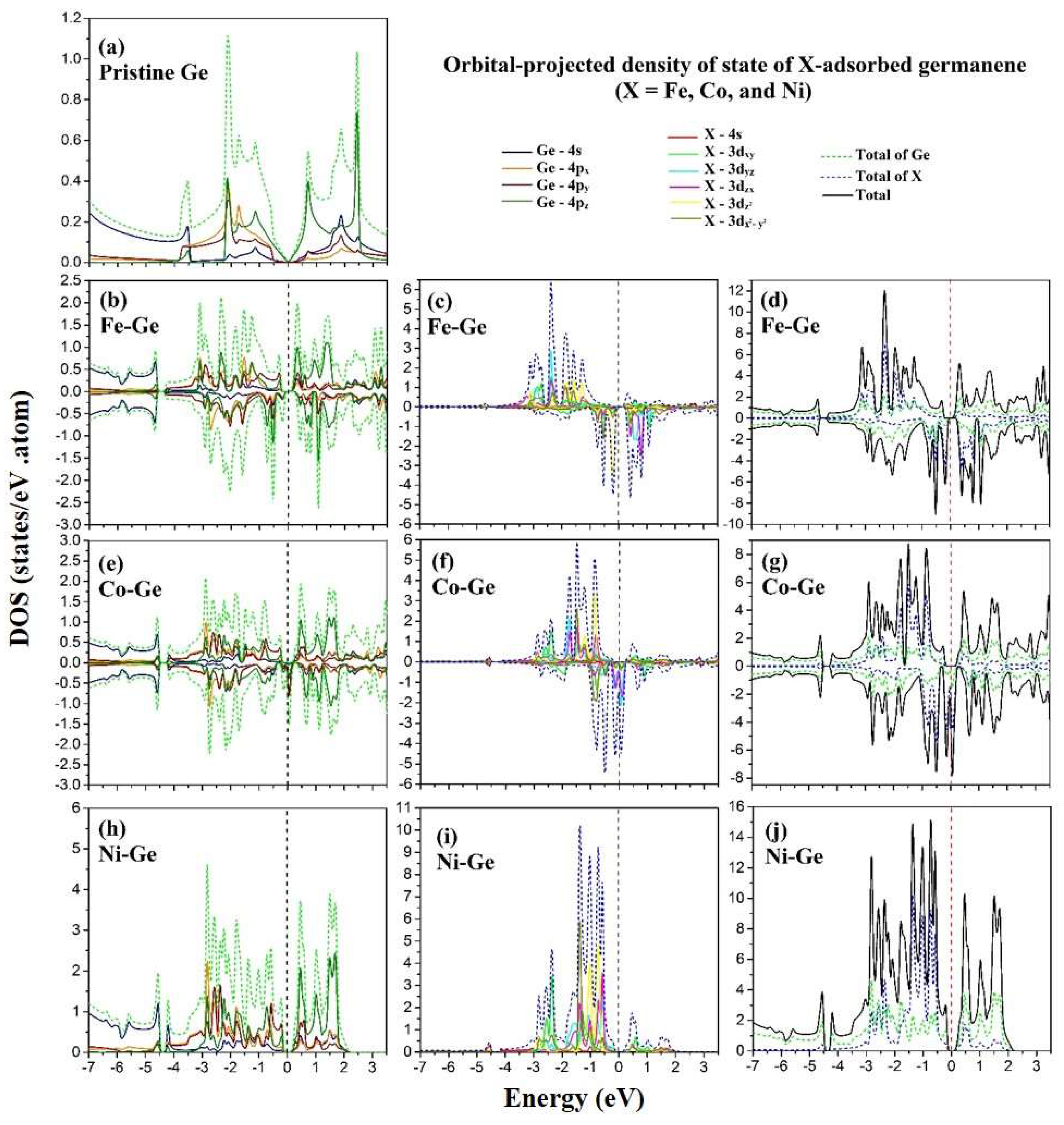
3.5. The Projected Density of States

The atom-, orbital-, and spin-decomposed DOS are useful to understand the orbital contributions and hybridizations. Various band-edge states of the electronic energy spectra can create diverse 2D van Hove singularities, as shown in Figure 6a–j. The critical points in the energy-wave-vector space (Figure 3a–d) cover the Dirac-cone bottoms, the extreme states of the parabolic dispersions, the saddle points/flat or partially flat subbands, and the constant-energy loops. Such electronic states generate V-shaped structures, shoulders, logarithmically symmetric peaks, and square-root-form asymmetric peaks, respectively, in the DOS. In pristine germanene, the asymmetric V-shaped structure is created by the modified Dirac cone in −0.5 eV < E < 0.5 eV eV due to the Ge-4 p z orbitals (Figure 6a). However, the V-shaped structure completely disappears when TM atoms are adsorbed. The Fe–Ge and Ni–Ge systems exhibit zero DOS at E F = 0 , demonstrating semiconductor behavior. As for the Co-Ge system, a high value of DOS appears at E F = 0 due to the crossings of partially flat subbands, suggesting the metallic character.
The prominent van Hove singularities near E F = 0 arise from the multi-hybridizations between the (4s, 4 p x , 4 p y , 4 p z ) orbitals of Ge and the (3 d x 2 y 2 , 3 d x y , 3 d y x , 3 d x z , 3 d z 2 ) orbitals of TM atoms for TM–Ge bonds. Single-orbital-dominated subbands do not exist in any of the adsorbed germanene systems. The four/six orbitals of the host and guest atoms might overlap at certain energies, illustrating the multi-orbital hybridizations in any chemical bond. The spin-split DOS (the spin-up and-down states are plotted in DOS < 0 and DOS > 0 , respectively) show that the strong ferromagnetic configurations occur near E F = 0 . At lower/higher energies, the spin-up and spin-down states coexist for the Ge DOS, but the opposite is true for the TM DOS. When E < 3 eV, the contribution of TM atoms to the DOS becomes negligible, and the spin-polarization totally disappears. The main features of the DOS could be validated by STS measurements (tunneling conductance d I / d V ) [47,48]. This powerful tool has been successfully used to explore diverse electronic properties in graphene-like systems [49,50].

4. Conclusions

The geometric and electronic properties of Fe-/Co-/Ni-adsorbed germanene were investigated using the first-principles calculations. The multi-orbital hybridizations between the (4s, 4 p x , 4 p y , 4 p z ) orbitals of Ge atoms and the (3 d x 2 y 2 , 3 d x y , 3 d y x , 3 d x z , 3 d z 2 ) orbitals of Fe/Co/Ni adatoms create a non-uniform chemical environment that enriches the electronic properties. The low-energy bands are mainly dominated by the TM atoms and present unusual energy dispersions, such as flat or partially flat subbands, with metallic or indirect-gap semiconductor behavior. Furthermore, the spin-split subbands around E F = 0 demonstrate the ferromagnetic configurations of Fe–Ge and Co–Ge systems. The feature-rich energy bands are reflected in the van Hove singularities in the DOS, such as shoulders, logarithmically symmetric peaks, and square-root-form asymmetric peaks. The orbital-decomposed and spin-split DOS provide critical information about multi-orbital hybridizations and the distinct spin polarizations between TM and Ge atoms. The simulation and analysis can be extended to more complex functionalized germanene systems, such as double-sided adsorption or doping with two or more types of guest adatoms simultaneously. In addition to adsorption, several events can occur during experimental growth, such as guest atom substitutions, defects, and heterojunctions, which are also worthy of careful investigation.

Author Contributions

Conceptualization, H.-Y.L. and J.-Y.W.; methodology, H.-Y.L.; software, H.-Y.L.; validation, H.-Y.L.; formal analysis, H.-Y.L. and J.-Y.W.; investigation, H.-Y.L. and J.-Y.W.; resources, J.-Y.W.; data curation, H.-Y.L.; writing—original draft preparation, H.-Y.L.; writing—review and editing, J.-Y.W.; visualization, H.-Y.L. and J.-Y.W.; supervision, J.-Y.W.; funding acquisition, J.-Y.W. All authors have read and agreed to the published version of the manuscript.

Funding

This work was supported by the National Science Council of Taiwan (Grant No. 107-2112- M-194-010-MY3) (Grant No. MOST 110-2112-M-992-001).

Institutional Review Board Statement

Not applicable.

Informed Consent Statement

Not applicable.

Data Availability Statement

The data presented in this study are available on request from the corresponding author.

Conflicts of Interest

The authors declare no conflict of interest.

References

  1. Pham, H.D.; Gumbs, G.; Su, W.P.; Tran, N.T.T.; Lin, M.F. Unusual features of nitrogen substitutions in silicone. Rsc. Adv. 2020, 10, 32193–32201. [Google Scholar] [CrossRef] [PubMed]
  2. Pflugradt, P.; Matthes, L.; Bechstedt, F. Unexpected symmetry and AA stacking of bilayer silicene on Ag(111). Phys. Rev. B 2014, 89, 205428–205432. [Google Scholar] [CrossRef]
  3. Shen, M.; Zhang, Y.Y.; An, X.T.; Liu, J.J.; Li, S.S. Valley polarization in graphene-silicene-graphene heterojunction in zigzag nanoribbon. J. Appl. Phys. 2014, 115, 233702. [Google Scholar] [CrossRef] [Green Version]
  4. Ye, M.; Quhe, R.; Zheng, J.X.; Ni, Z.Y.; Wang, Y.Y.; Yuan, Y.K.; Tse, G.; Shi, J.J.; Gao, Z.X.; Lu, J. Tunable band gap in germanene by surface adsorption. Phys. E 2014, 59, 60–65. [Google Scholar] [CrossRef] [Green Version]
  5. Lee, K.W.; Lee, C.E. Spin-orbit coupling-induced band inversion and spin Chern insulator phase in plumbene and stanine. Curr. Appl. Phys. 2020, 20, 413–418. [Google Scholar] [CrossRef]
  6. Kuzmany, H.; Shi, L.; Martinati, M.; Cambre, S.; Wenseleers, W.; Kurti, J.; Koltai, J.; Kukucska, G.; Cao, K.C.; Kaiser, U.; et al. Well-defined sub-nanometer graphene ribbons synthesized inside carbon nanotubes. Carbon 2021, 171, 221–229. [Google Scholar] [CrossRef]
  7. Usachov, D.Y.; Fedorov, A.V.; Vilkov, O.Y.; Senkovskiy, B.V.; Adamchuk, V.K.; Andryushechkin, B.V.; Vyalikh, D.V. Synthesis and electronic structure of nitrogen-doped graphene. Phys. Solid State 2013, 55, 1325–1332. [Google Scholar] [CrossRef]
  8. Ileri, N.; Goldman, N. Graphene and nano-diamond synthesis in expansions of molten liquid carbon. J. Chem. Phys. 2014, 141, 164709–164714. [Google Scholar] [CrossRef] [Green Version]
  9. Du, M.; Xu, C.H.; Sun, J.; Gao, L. One step synthesis of Fe2O3/nitrogen-doped graphene composite as anode materials for lithium ion batteries. Electrochim. Acta 2012, 80, 302–307. [Google Scholar] [CrossRef]
  10. Zhi-Gang Shao, Z.G.; Ye, X.S.; Yang, L.; Wang, C.L. First-principles calculation of intrinsic carrier mobility of silicene. J. Appl. Phys. 2013, 114, 93712–93715. [Google Scholar] [CrossRef]
  11. Cinquanta, E.; Fratesi, G.; Conte, S.D.; Grazianetti, C.; Scotognella, F.; Stagira, S.; Vozzi, C.; Onida, G.; Molle, A. Optical response and ultrafast carrier dynamics of the silicene-silver interface. Phys. Rev. B 2015, 92, 165427–165431. [Google Scholar] [CrossRef] [Green Version]
  12. Cahangirov, S.; Topsakal, M.; Akturk, E.; Sahin, H.; Ciraci, S. Two- and One-Dimensional Honeycomb Structures of Silicon and Germanium. Phys. Rev. Lett. 2009, 102, 236804–236807. [Google Scholar] [CrossRef] [PubMed] [Green Version]
  13. Shukla, A.; Kumar, R.; Mazher, J.; Balan, A. Graphene made easy: High quality; large-area samples. Solid State Commun. 2009, 149, 718–721. [Google Scholar] [CrossRef] [Green Version]
  14. Zhang, L.; Liang, J.J.; Huang, Y.; Ma, Y.F.; Wang, Y.; Chen, Y.S. Size-controlled synthesis of graphene oxide sheets on a large scale using chemical exfoliation. Carbon 2009, 47, 3365–3368. [Google Scholar] [CrossRef]
  15. Chen, L.; Hernandez, Y.; Feng, X.L.; Mullen, K. From Nanographene and Graphene Nanoribbons to Graphene Sheets: Chemical Synthesis. Angew. Chem. Int. Ed. 2012, 51, 7640–7654. [Google Scholar] [CrossRef]
  16. Ogikubo, T.; Shimazu, H.; Fujii, Y.; Ito, K.; Ohta, A.; Araidai, M.; Kurosawa, M.; Lay, G.L.; Yuhara, J. Continuous Growth of Germanene and Stanene Lateral Heterostructures. Adv. Mater. Interfaces 2020, 7, 1902132. [Google Scholar] [CrossRef]
  17. Ge, M.; Zong, M.; Xu, D.; Chen, Z.; Yang, J.; Yao, H.; Wei, C.; Chen, Y.; Lin, H.; Shi, J. Freestanding germanene nanosheets for rapid degradation and photothermal conversion. Mater. Today Nano 2021, 15, 100119. [Google Scholar] [CrossRef]
  18. Si, X.; She, W.; Xu, Q.; Yang, G.; Li, Z.; Wang, S.; Luan, J. First-Principles Density Functional Theory Study of Modified Germanene-Based Electrode Materials. Materials 2022, 15, 103. [Google Scholar] [CrossRef]
  19. Hussain, T.; Kaewmaraya, T.; Chakraborty, S.; Vovusha, H.; Amornkitbamrung, V.; Ahuja, R. Defected and Functionalized Germanene-based Nanosensors under Sulfur Comprising Gas Exposure. ACS Sens. 2018, 3, 867–874. [Google Scholar] [CrossRef] [Green Version]
  20. Ullah, F.; Irshad, S.; Khan, S.; Hashmi, M.A.; Ludwig, R.; Mahmood, T.; Ayub, K. Nonlinear optical response of first-row transition metal doped Al12P12 nanoclusters; a first-principles study. J. Phys. Chem. Solids 2021, 151, 109914. [Google Scholar] [CrossRef]
  21. Irshada, S.; Ullaha, F.; Khana, S.; Ludwigb, R.; Mahmooda, T.; Ayub, K. First row transition metals decorated boron phosphide nanoclusters as nonlinear optical materials with high thermodynamic stability and enhanced electronic properties; A detailed quantum chemical study. Opt. Laser Technol. 2021, 134, 106570. [Google Scholar] [CrossRef]
  22. Ullah, F.; Ayub, K.; Mahmood, T. High performance SACs for HER process using late first-row transition metals anchored on graphyne support: A DFT insight. Int. J. Hydrogen Energy 2021, 46, 37814–37823. [Google Scholar] [CrossRef]
  23. Sun, M.; Ren, Q.; Wang, S.; Zhang, Y.; Du, Y.; Yu, J.; Tang, W. Magnetism in transition-metal-doped germanene: A first-principles study. Comput. Mater. Sci. 2016, 118, 112–116. [Google Scholar] [CrossRef]
  24. Zhou, P.; Sun, L.Z. 3d Transition Metal Adsorption Induced the valley-polarized Anomalous Hall Effect in Germanene. Sci. Rep. 2016, 6, 27830. [Google Scholar] [CrossRef]
  25. Lin, Z.Z.; Chen, X. Transition-metal-decorated germanene as promising catalyst for removing CO contamination in H2. Mater. Des. 2016, 107, 82–89. [Google Scholar] [CrossRef]
  26. Kaloni, T.P. Tuning the Structural, Electronic, and Magnetic Properties of Germanene by the Adsorption of 3d Transition Metal Atoms. J. Phys. Chem. C 2014, 118, 25200–25208. [Google Scholar] [CrossRef] [Green Version]
  27. Pang, Q.; Li, L.; Zhang, C.L.; Wei, X.M.; Song, Y.L. Structural, electronic and magnetic properties of 3d transition metal atom adsorbed germanene: A first-principles study. Mater. Chem. Phys. 2015, 160, 96–104. [Google Scholar] [CrossRef]
  28. Nemoto, R.; Kruger, P.; Hartini, A.N.P.; Hosokai, T.; Horie, M.; Kera, S.; Yamada, T.K. Well-Ordered Monolayer Growth of Crown-Ether Ring Molecules on Cu(111) in Ultra-High Vacuum: An STM; UPS; and DFT Study. J. Phys. Chem. C 2019, 123, 18939–18950. [Google Scholar] [CrossRef]
  29. Heidarzadeh, A. Tensile behavior; microstructure; and substructure of the friction stir welded 70/30 brass joints: RSM; EBSD; and TEM study. Arch. Civ. Mech. Eng. 2019, 19, 137–146. [Google Scholar] [CrossRef]
  30. Cheng, Z.W.; Zhang, Z.Y.; Sun, H.G.; Li, S.J.; Yuan, H.; Wang, Z.J.; Cao, Y.; Shao, Z.B.; Bian, Q.; Zhang, X.; et al. Visualizing Dirac nodal-line band structure of topological semimetal ZrGeSe by ARPES. Appl. Mater. 2019, 7, 051105. [Google Scholar] [CrossRef] [Green Version]
  31. Ridene, M.; Girard, J.C.; Travers, L.; David, C.; Ouerghi, A. STM/STS investigation of edge structure in epitaxial graphene. Surf. Sci. 2012, 606, 1289–1292. [Google Scholar] [CrossRef]
  32. Liu, X.; Wang, C.Z.; Yao, Y.X.; Lu, W.C.; Hupalo, M.; Tringides, M.C.; Ho, K.M. Bonding and charge transfer by metal adatom adsorption on graphene. Phys. Rev. B 2011, 83, 235411. [Google Scholar] [CrossRef]
  33. Hohenberg, P.; Kohn, W. Inhomogeneous Electron Gas. Phys. Rev. 1964, 136, B864–B871. [Google Scholar] [CrossRef] [Green Version]
  34. Kohn, W.; Sham, L.J. Self-Consistent Equations Including Exchange and Correlation Effects. Phys. Rev. 1965, 140, A1133–A1138. [Google Scholar] [CrossRef] [Green Version]
  35. Kresse, G.; Furthmuller, J. Efficient iterative schemes for ab initio total-energy calculations using a plane-wave basis set. Phys. Rev. B 1996, 54, 11169–11186. [Google Scholar] [CrossRef]
  36. Kresse, G.; Joubert, D. From ultrasoft pseudopotentials to the projector augmented-wave method. Phys. Rev. B 1999, 59, 1758–1775. [Google Scholar] [CrossRef]
  37. Perdew, J.P.; Burke, K. Generalized gradient approximation made simple. Phys. Rev. Lett. 1996, 77, 3865. [Google Scholar] [CrossRef] [Green Version]
  38. Blanc, X.; Cances, E.; Dupuy, M.S. Variational projector augmented-wave method. Comptes Rendus Math. 2017, 355, 665–670. [Google Scholar] [CrossRef]
  39. Li, S.S.; Zhang, C.W.; Ji, W.X.; Li, F.; Wang, P.J.; Hu, S.J.; Yan, S.S.; Liu, Y.S. Tunable electronic and magnetic properties in germanene by alkali, alkaline-earth, group III and 3d transition metal atom adsorption. Phys. Chem. Chem. Phys. 2014, 16, 15968–15978. [Google Scholar] [CrossRef]
  40. Naji, S.; Belhaj, A.; Labrim, H.; Bhihi, M.; Benyoussef, A.; Kenz, A.E. Adsorption of Co and Ni on Graphene with a Double Hexagonal Symmetry: Electronic and Magnetic Properties. J. Phys. Chem. C 2014, 118, 4924–4929. [Google Scholar] [CrossRef]
  41. Perdewa, J.P.; Yangc, W.; Burked, K.; Yanga, Z.; Grossf, E.K.U.; Schefflerg, M.; Scuseria, G.E.; Hendersonj, T.M.; Zhangg, I.Y.; Ruzsinszkya, A.; et al. Understanding band gaps of solids in generalized Kohn–Sham theory. Proc. Natl. Acad. Sci. USA 2017, 114, 2801–2806. [Google Scholar] [CrossRef] [PubMed] [Green Version]
  42. Rudenko, A.N.; Katsnelson, M.I.; Roldan, R. Electronic properties of single-layer antimony: Tight-binding model, spin-orbit coupling, and the strength of effective Coulomb interactions. Phys. Rev. B 2017, 95, 081407. [Google Scholar] [CrossRef] [Green Version]
  43. Phark, S.H.; Sander, D. Spin-polarized scanning tunneling microscopy with quantitative insights into magnetic probes. Nano Converg. 2017, 4, 8. [Google Scholar] [CrossRef] [PubMed] [Green Version]
  44. Matsuyama, H.; Nara, D.; Kageyama, R.; Honda, K.; Sato, T.; Kusanagi, K.; Srinivasan, E.; Koike, K. Spin-polarized scanning tunneling microscopy experiments on the rough surface of a polycrystalline NiFe film with a fine magnetic tip sensitive to a well-defined magnetization component. AIP Adv. 2016, 6, 035122. [Google Scholar] [CrossRef] [Green Version]
  45. Farrar, L.S.; Nevill, A.; Lim, Z.J.; Balakrishnan, G.; Dale, S.; Bending, S.J. Superconducting Quantum Interference in Twisted van der Waals Heterostructures. Nano Lett. 2021, 21, 6725–6731. [Google Scholar] [CrossRef]
  46. Giazotto, F.; Peltonen, J.T.; Meschke, M.; Pekola, J.P. Superconducting quantum interference proximity transistor. Nat. Phys. 2010, 6, 254–260. [Google Scholar] [CrossRef] [Green Version]
  47. Krenner, W.; Kuhne, D.; Klappenberger, F.; Barth, J.V. Assessment of Scanning Tunneling Spectroscopy Modes Inspecting Electron Confinement in Surface-Confined Supramolecular Networks. Sci. Rep. 2013, 3, 1454. [Google Scholar] [CrossRef] [Green Version]
  48. Ting, W.; Egi, T.; Itti, R.; Kuroda, K.; Koshizuka, N.; Tanaka, S. STM/STS measurements on clean and stable surfaces of as-prepared Nd1Ba2Cu3Oy single crystals. Phys. C Supercond. 1996, 263, 185–188. [Google Scholar] [CrossRef]
  49. Phark, S.H.; Borme, J.; Vanegas, A.L.; Corbetta, M.; Sander, D.; Kirschner, J. Scanning tunneling spectroscopy of epitaxial graphene nanoisland on Ir(111). Nanoscale Res. Lett. 2012, 7, 255–258. [Google Scholar] [CrossRef]
  50. Klusek, Z.; Dabrowski, P.; Kowalczyk, P.; Kozlowski, W.; Olejniczak, W.; Blake, P.; Szybowicz, M.; Runka, T. Graphene on gold: Electron density of states studies by scanning tunneling spectroscopy. Appl. Phys. Lett. 2009, 95, 113114. [Google Scholar] [CrossRef]
Figure 1. The side and top views of optimal geometric structures for (a) pristine germanene, (b) iron-, (c) cobalt-, and (d) nickel-adsorbed germanenes.
Coatings 12 00948 g001
Figure 2. Four possible adsorption sites: top (1), hollow (2), bridge (3), and valley (4).
Coatings 12 00948 g002
Figure 3. Band structures with the atom contributions for (a) pristine germanene, (b) cobalt-, (c) iron-, and (d) nickel-adsorbed germanenes.
Coatings 12 00948 g003
Figure 4. Spatial charge density (ad) and charge density difference (eg) for pristine germanene, iron-, cobalt-, and nickel-adsorbed germanenes, respectively.
Coatings 12 00948 g004
Figure 5. The spin–charge distributions of (a) iron- and (b) cobalt-adsorbed germanenes. Red and yellow correspond to spin up and down, respectively.
Coatings 12 00948 g005
Figure 6. The atom-, orbital-, and spin-projected density of states for (a) pristine germanene, (bd) iron-, (eg) cobalt-, and (hj) nickel-absorbed germanenes.
Coatings 12 00948 g006
Table 1. The optimal geometric structures of iron-, cobalt-, and nickel-adsorbed germanene systems for the adsorption energies E a d s , the distance of adatom to germanene layer h, X–Ge bond lengths (X = Fe, Co, Ni), Ge–Ge bond lengths, magnetic moments, and the buckling height.
AdatomsSites E ads (eV)h (Å)X–Ge (Å)Ge–Ge (Å)Magnetic Moment ( μ B )Buckling Height (Å)
Pristine 2.42 0.66
Valley3.06
IronHollow3.431.022.454, 2.7102.6512.731.13
Top2.65
Valley3.60
CobaltHollow4.201.052.437, 2.7182.5951.751.12
Top3.75
Valley1.19
NickelHollow1.850.952.436, 2.6492.55201.35
Top1.50
Publisher’s Note: MDPI stays neutral with regard to jurisdictional claims in published maps and institutional affiliations.

