Article

Optimization of the Thickness and Interface Structure of Al2O3-YAG/ZrO1.5-YO1.5-TaO1.5/8YSZ/NiCoCrAlY Multilayer Thermal Barrier Coatings: A Finite Element Simulation

1
School of Mechanical Engineering, Qinghai University, Xining 810016, China
2
Integrated Computational Materials Research Centre, Shanghai Institute of Ceramics, Chinese Academy of Sciences, Shanghai 201899, China
*
Authors to whom correspondence should be addressed.
Coatings 2022, 12(11), 1660; https://doi.org/10.3390/coatings12111660
Submission received: 30 September 2022 / Revised: 27 October 2022 / Accepted: 28 October 2022 / Published: 1 November 2022

Abstract

:

Highlights

(1) 
The thickness and interface structure of the multilayer ceramic layers were optimized using the finite element method, which significantly saved the cost of experiments.
(2) 
The failure mechanism and thickness selection range of the multilayer coatings were determined, providing theoretical guidance for the coating process.
(3) 
The effects of different roughness on the magnitude and distribution of interfacial residual stresses were investigated to provide theoretical guidance for the selection of interfacial roughness of thermal sprayed coatings.

Abstract

Thermal barrier coatings (TBCs) prepared using the atmospheric plasma spraying method fail mainly due to coating delamination caused by thermal mismatch in the absence of high temperature assessment. In this study, the thickness optimization of multiple ceramic layers in a TBCs and the influence of the interface structure on the residual stress of the coating were investigated using a finite element simulation method. The results showed that varying the thickness of each layer of a TBCs with multiple ceramic layers affects the distribution and magnitude of the residual stress of the coating. Therefore, a reasonable range of thickness for each layer can be determined. The thickness of the bonding layer should be 110 μm, the thickness of YSZ layer should be about 270 μm, the thickness of tantalate layer should be about 70 μm, and the thickness of Al2O3-YAG layer should be about 100 μm. Simultaneously, the results show that a rough interface can be more effective in reducing the relief of stress concentrations compared to a smooth interface, but the stress values increase.

1. Introduction

Thermal barrier coatings (TBCs) are ceramic coatings that are deposited on the surface of a high-temperature-resistant metal. They play an important role in insulating the substrate and in reducing the operating temperature of the substrate. A workpiece with this type of coating (such as an engine turbine blade) can operate at high temperatures, and the heat efficiency of a workpiece, such as an engine, can be increased by approximately 60%. Thermal barrier coatings are currently being utilized in various engineering areas, which include internal combustion engines, gas turbine blades of jet engines, pyrochemical reprocessing units and many more [1]. Ceramic coatings are resistant to high temperatures due to their inert properties and resistance. The ceramic coatings are usually prepared by air plasma spraying (APS) processes and electron beam physical vapor deposition (EB-PVD), and this paper focuses on finite element simulation of thermal barrier coatings prepared by APS [2].
The structure of a traditional TBC consists of a superalloy substrate (SUB) layer, bonding (BC) layer, thermally grown oxide (TGO) layer, and the ceramic top (TC) layer. A detailed structure is shown in Figure 1. The TC layer is located on the outermost surface of the whole TBC, and its thickness is generally in the range of 100~400 μm. It has the characteristics of low thermal conductivity, high melting point, corrosion resistance, and excellent thermal shock resistance. Its main chemical composition is yttria-stabilized zirconia (YSZ) with a yttria mass fraction of 6~8%. The thickness of the BC layer is 100~200 μm. The layer between the TC and SUB layers is primarily composed of MCrAlY, which is coated and plays an important role in protecting the substrate and bonding the TC layer to the substrate. The thermal expansion coefficient (CTE) of this layer is between the TC and the SUB layers, and the large difference in this CTE relieves the thermal mismatch. The thickness of the TGO layer is in the range of 1~10 μm and the main component is α-Al2O3, which has high densification [3]. An example of high-temperature-resistant alloy substrate material is a nickel-based single-crystal superalloy that can withstand the mechanical load of the blade [4]. However, when the operating temperature of TBCs was increased, YSZ experienced a phase transition at 1200 °C. This resulted in a significantly large volume change, a significant subsequent thermal stress in the coating, and finally, coating failure [5,6,7,8]. Therefore, traditional TBCs with a single TC layer cannot meet the current requirements, and it is necessary to develop a new type of TBC with multiple TC layers. This new coating should be designed to better adapt to new application environments with better thermal insulation performance [9]. When selecting the coating material, the following conditions should be met: First, the coating must have high resistance to reaction with oxidizing substances. The coefficient of thermal expansion (CTE) of the coating should be close to the base material, preventing any delamination or cracking due to CTE mismatch. Third, it should be chemically stable under high operating conditions, and the coating composition should be chemically inert to the base material [10]. To reduce the thermal mismatch between the TC layer and the substrate, it is necessary to design a multilayer structure. This coating material was selected based on the selection principle for oxide ceramic materials with low thermal conductivities, as proposed by Professor Clarke at Harvard University [11].
Because of its high melting point, low thermal conductivity, high thermal expansion coefficient, good high-temperature phase stability, and excellent mechanical properties, rare earth tantalate is expected to become a new TBC material. Studies on ZrO2-YO1.5-TaO2.5 have shown that these properties change with the proportion of yttria and tantalum oxide [12,13,14,15,16]. There are three chemical formulas for tantalate: YTaO4, Y3TaO7, and YTa3O9. Previous calculation results about its thermal conductivity have shown that the minimum thermal conductivity was 1.0 W∙K−1∙m−1, which is much lower than those of the YSZ ceramics (2.0~3.0 W∙K−1∙m−1) currently used. An extremely low thermal conductivity provides better insulation, thereby increasing the service temperature.
An α-Al2O3 coating has a low oxygen diffusion rate and high-density hcp crystal structure. Although they provide high-temperature oxidation protection ability [17,18,19], the complex phase transition and high internal stress of these coatings make them prone to cracking or shedding during thermal of high-temperature cycling. Yttrium aluminum garnet (Y3Al5O12, YAG) is a compound formed by the solid-state reaction of Al2O3 and Y2O3 [20,21]. It has good high-temperature creep resistance and excellent thermal–mechanical properties above 1800 °C [22,23]. Therefore, numerous studies have shown that YAG can improve the anti-creep and mechanical properties of α-Al2O3. The bonding strength of the eutectic coating remained partially unchanged with a large displacement, and the compressive creep strength at 1873 K was approximately 10 times higher than that of a sintered composite with the same composition. Even when heated at 1973 K for 50 h and then exposed for 1000 h, the microstructure did not change [24,25,26,27]. Therefore, it is available for the design of multilayer ceramic layer TBCs using these materials. The ceramic layers should be designed to reduce the excessive thermal stress concentration caused by a large CTE mismatch.
Low residual stress and high thermal insulation are important parameters for evaluating the coating performance. Several factors can affect the stress distribution and heat insulation effects, such as thermal conductivity, CTE, interface morphology, coating thickness, elastic modulus, internal defects, heat convection between each layer [28,29,30,31,32], and air. Sarikaya et al. studied the interlayers and bonding layer of the MgO-ZrO2 coating system and concluded that increasing the interlayer number would reduce the thermal stress of the coating system and improve the thermal insulation ability [33]. Rätzer-Scheibe et al. [34] studied the effect of coating thickness on the thermal conductivity of partially Y2O3-stabilized zirconia (PYSZ) fabricated by electron beam physical vapor deposition (EB-PVD). They found that a thin independently applied PYSZ coating was fragile. The new sample type with a coating thickness of less than 200 μm is called a “quasi-independent” coating. This sample was composed of a PYSZ coating and a sapphire disk as the substrate for the sensitive coating. Because sapphire is transparent to the laser, this sample was similar to a real independent coating. In contrast to the measurement of the two-layer samples, the thermal conductivity of the independent PYSZ coating was sensitive to the coating thickness, which increased with increasing thickness. The thermal conductivity of the coating with the thickness of 300 μm was approximately 40% higher than that of a 50 μm coating. Therefore, the coating thickness had a significant influence on the residual stress distribution and thermal insulation performance of the coating. If the coating is too thin, it does not exhibit the ideal thermal insulation effect. If the coating is too thick, the residual stress increases with the coating thickness. Thus, optimization of the coating thickness is crucial [33,34,35]. Additionally, the influence of the interface morphology of the coating on the distribution and amplitude residual stress of the TBCs was evident. Ranjbar-Far [36] used the finite element method (FEM) to evaluate the thermal cycling stress in a typical plasma-sprayed TBC system. The thermodynamic model of the system considered the effects of the thermal and mechanical properties, morphology of the topcoat/bond coat interface, and oxidation on the local stress. These stresses led to the nucleation of microcracks during cooling, particularly near the metal/ceramic interface. the effects of the geometric morphology and abnormal amplitude on the stress distribution was studied based on the different interface roughness shapes corresponding to two-dimensional and periodic geometries. It was found that the compressive stress was significantly higher in the trough, and the crack did not propagate until the trough region. With increasing amplitude, the quantitative value of stress increased. With the thickness of the TGO layer increasing, a tensile stress region will be formed between the bond coat layer and the top-coat, resulting in crack propagation at the TGO/BC and TBCs/TGO interfaces. Although a rough interface in the coating system improved the adhesion of the coating. During thermal cycling, the life of a plasma-sprayed TBC system can be improved by the compression zone [37,38]. However, many studies have shown that the maximum stress in TBCs occurs at the TBCs/BC interface during thermal cycling. A rough interface in a coating system also increases its tensile stress level or region [39,40,41].
Herein, thickness optimization of multilayer ceramic layers and the design of the interface morphology were simulated and calculated. The simulation results showed that the thickness of the multiple ceramic layers and the influence of the interface morphology on the residual stress distribution could be used to determine the optimal coating thickness and appropriate roughness, which could provide a guide for the selection of the optimal coating thickness of such a multilayer ceramic coating in the future.

2. Materials and Methods

This section discusses the design and optimization process of the TBCs via for finite element simulation. The finite element simulation process primarily included the establishment of the design model and application of appropriate boundaries and initial conditions. The objective of the optimization process is to determine the appropriate coating structure model and thickness by reviewing whether the coating failed base on the magnitude of the residual stress.

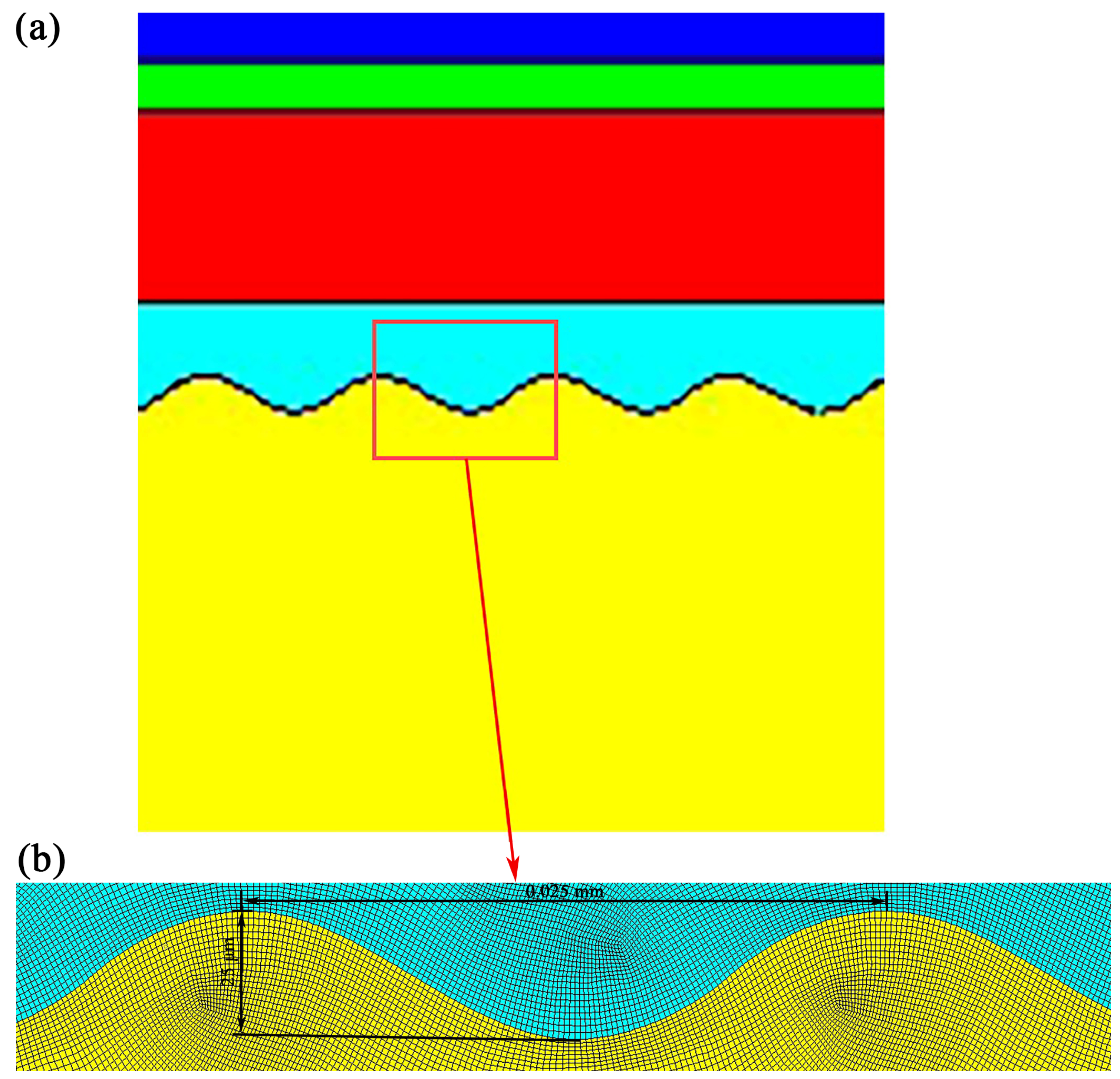
2.1. Finite Element Simulation Model

The model was established based on the actual usage of the TBCs and its thermal expansion coefficient, considering the heat transfer mechanisms of heat conduction and convection, as shown in Figure 2a. Figure 3a shows the finite element model after changing the interface structure, and Figure 3b shows the enlarged schematic of the mesh of 3a at the interface location.
In this study, a thermal–mechanical coupling analysis step was used to calculate the residual stress of the TBCs, and the following assumptions were made: (1) All layers were isotropic, none of the layers had defects, and the interface between two adjacent layers was flat. (2) Heat transfer only occurred in the coating with air through upper-surface convection, and the side was adiabatic without considering thermal radiation. (3) The deformation of the entire coating system was assumed to be continuous without considering defects such as cracks and pores. (4) The creep and plastic deformation of each layer were negligible. (5) In thermal barrier coatings, failure can be divided into two cases, one is caused by thermal stress mismatch, and the other is caused by thermally grown oxide (TGO). This paper studies the post-spraying cooling process, rather than sustained high-temperature service process. Therefore, in these two failure mechanisms, the thermal mismatch leads to the interface separation failure of the coating, and the effect of TGO can be ignored [42]. (6) There is no heat resistance at the interfaces between adjacent layers [43].
The Ansys APDL approach enables parametric modeling, application of parametric loads and solutions, and display of processing results after parametrization, thus realizing the whole process of parametric finite element analysis. The whole process of parametric finite element analysis is realized. In the parametric analysis, the parameters can be simply modified to achieve repeated analysis of various sizes, different loads or sequential products of various sizes and loads, which can greatly improve the analysis efficiency and reduce the analysis cost [44]. Based on this model, a two-dimensional symmetric finite element numerical model without a TGO layer was established using the finite element commercially available software ANSYS with the two-dimensional four-node thermal structure coupling element PLANE 13. The numerical model is divided into five layers. The bottom layer was the SUB layer, followed by the BC, bottom ceramic (TC3), middle ceramic (TC2), and top ceramic (TC1) layers. A 1:1 mesh was used, with mesh refinement near the layer interfaces to improve the calculation accuracy, with a grid size of 1e-6 m, as shown in Figure 2b,c. In recent studies, the thickness of the bond-coat layer was approximately 100~200 μm, and the thickness of the ceramic layer was approximately 100~400 μm [3,42,45,46,47]. Therefore, 100–200 μm was selected as the bond-coat layer thickness of the model in this study, and the thickness of each ceramic layer was optimized in the range of 100~400 μm.

2.2. Boundary Conditions

In this study, multi-point coupling was used to calculate the stress of the coating from high temperature to room temperature, which can be regarded as a heat-coat cycle. When using a two-dimensional plane model, the thickness of the coating on the blade is infinitely small relative to the blade size in the other directions. Thus, in most cases, the heat transfer was considered to be in the thickness direction of the coating, also called the spray direction [45]. Therefore, heat convection between the surface of the coating and the air exchange occurred only at the top of the sample. The convection coefficient was set as 150 W/(m2∙K), and the cooling time was 1800 s. The bottom and sides of the sample were adiabatic. The initial temperature of the coating was set to 1300 °C, the displacement constraint UY = 0 was imposed onto the bottom of the sample, and the displacement constraint UX = 0 was imposed onto the left side of the model.

2.3. Material Thermo-Physical Performance Parameters

The material performance parameters of the GH3128, MCrAlY bond layer, 8YSZ, tantalate, Al2O3, and YAG used in this study are listed in Table 1, Table 2, Table 3, Table 4, Table 5 and Table 6 [48,49,50,51,52,53,54]. The tantalate parameters were obtained by testing ZrO1.5-YO1.5-TaO1.5 bulk samples prepared in the experiments. The main purpose of this study is to analyze the influence of the thickness of multiple ceramic layers and their interface structure characteristics on the distribution and magnitude of stress. In this study, the stress and strain of the coating were generated due to a change in the temperature. Therefore, without considering the changes in material properties as a function of temperature, the properties of each layer are independent of temperature. For the plane strain thermal stress, the elastic body temperature can be set as T, and the isotropic material is freely telescopic without constraint. If α is the thermal expansion coefficient of the material, the material produces a positive strain expressed as αT. The deformation components of each point in the elastic body were εx = εy = αT and γxy = 0. μ represents the temperature distribution at any point. Thermal stress occurs when the above deformation cannot freely occur. Thus, the total deformation component is calculated as follows:
ε x = ( σ x μ σ y ) E + α T ,
ε y = ( σ y μ σ x ) E + α T ,
γ x y = 2 ( 1 + μ ) E τ x y ,
The above equation is the physical equation of the thermoelastic plane stress represented by the stress component and temperature difference.
The stress component is expressed by the deformation component and variable temperature T, and the physical equation can be expressed as follows:
σ x = E ( 1 μ 2 ) ( ε x + μ ε y ) E a T ( 1 μ ) ,
σ y = E ( 1 μ 2 ) ( ε y + μ ε x ) E a T ( 1 μ ) ,
τ x y = E 2 ( 1 + μ ) γ x y ,
The geometric equation of the plane problem is still expressed as follows:
ε x = u x , ε y = ν y , γ x y = u y + ν x ,
The geometric equation is introduced into the physical equation, and the stress component is represented by the displacement component and variable temperature T as follows:
σ x = E ( 1 μ 2 ) ( u x + μ ν y ) E a T ( 1 μ ) ,
σ y = E ( 1 μ 2 ) ( ν y + μ u x ) E a T ( 1 μ ) ,
τ x y = E 2 ( 1 + μ ) ( ν x + u y ) ,
The above equation can be substituted into the equilibrium differential equation regardless of the physical force:
σ x x + τ y x y = 0 ,
σ y y + τ x y x = 0 ,
A differential equation for solving the plane stress problem of thermal stress is obtained after simplification:
2 u x 2 + ( 1 u ) 2 2 u y 2 + ( 1 + u ) 2 2 ν x y ( 1 + u ) a T x = 0 ,
2 ν y 2 + ( 1 u ) 2 2 ν x 2 + ( 1 + u ) 2 2 u x y ( 1 + u ) a T y = 0 ,
The solution of a thermoelastic problem should not only satisfy the above basic thermodynamic equations but also the corresponding definite solution conditions. The definite solution conditions are classified as the force and displacement boundary conditions. m, l are the weight coefficient of the stress components in the x, y directions, respectively. The stress boundary condition of the plane problem is expressed as:
σ x l + τ y x m = X ¯ ,
σ y m + τ x y l = Y ¯ ,
The displacement boundary conditions can be expressed as follows:
u = u ¯ ( x , y ) , ν = ν ¯ ( x , y ) ,
Here, u ¯ ( x , y ) , ν ¯ ( x , y ) is the boundary displacement function [55].
A solution can be obtained for the plane-strain problem of thermal stress as follows:
E = E ( 1 μ 2 ) , μ = μ ( 1 μ 2 ) , a = a ( 1 + μ ) ,
We can assume that the substrate thickness is HS, the thickness of bond-coat is HBC, and the thickness of ceramic layer is HTC. Hsueh [51] showed that for an axisymmetric TBCs model, the axisymmetric stress produces bending when the coating is cooled from high temperature to room temperature. The coating strain can be divided into two components: uniform and bending.
ε = c + ( Z H b ) r , ( H S H H B C + H T C ) ,
where c is the uniform component of the strain, ZHb is the value of Z when the bending component of the coating is zero, and r is the curvature radius of the layer. The effect of pure bending was considered, whereas the shear deformation was ignored. Because the thermal strain is f and the coating is not subject to external constraints, the stress–strain relationships of the substrate, bond-coat layer, and ceramic layer are as follows:
Relationship between stress and strain of substrate:
σ S = E S ( c + ( Z H b ) r α S Δ T ) , ( H S Z 0 ) ,
Relationship between stress and strain of bond-coat layer:
σ B C = E B C ( c + ( Z H b ) r α B C Δ T ) , ( 0 Z H B C ) ,
Relationship between stress and strain of ceramic layer:
σ T C = E T C ( c + ( Z H b ) r α T C Δ T ) , ( H B C Z H B C + H T C ) ,
In the above equations, E i = E i ( 1 υ i ) , ES, EBC, and ETC are the elastic modulus of the substrate, bond-coat layer, and ceramic layer, respectively, and υi is Poisson’s ratio for each material. αS, αBC, and αTC are the thermal expansion coefficients of the substrate, bond-coat layer, and ceramic layer, respectively, and c, Hb, and r are determined by boundary conditions.
Boundary condition 1: The uniform component of strain makes the resultant force zero.
E S ( c α S Δ T ) H S U B + E B C ( c α B C Δ T ) H B C + E T C ( c α T C Δ T ) H T C = 0 ,
It can be further expressed as the following:
c = ( E S H S α S U B + E T C H T C α T C + E B C H B C α B C ) Δ T E S H S + E T C H T C + E B C H B C ,
Boundary condition 2: The bending component of the strain causes the resultant force to become zero.
H S 0 E S ( Z H b ) r d Z + 0 H B C E B C ( Z H b ) r d Z + H B C H B C + H T C E T C ( Z H b ) r d Z = 0 ,
It can be expressed as follows:
H b = ( E s H S 2 + E T C H T C ( 2 H B C + H T C ) + E B C H B C 2 ) 2 ( E S H S + E T C H T C + E B C H B C ) ,
Boundary condition 3: The sum of the bending moments of the bending axes of the substrate, bond-coat layer, and ceramic layer was determined to be zero.
H S 0 σ S ( Z H b ) d Z + 0 H B C σ B C ( Z H b ) d Z + H B C H B C + H T C σ T C ( Z H b ) d Z = 0 ,
It can be express as follows:
1 r = 3 ( E S ( c α S Δ T ) H S 2 E T C H T C ( c α T C Δ T ) ( 2 H B C + H T C ) E B C H B C 2 ( c α B C Δ T ) ) E S H S 2 ( 2 H S + 3 H b ) + E T C H T C [ 6 H B C 2 + 6 H B C H T C + 2 H T C 2 3 H b ( 2 H B C + H T C ) ] + 2 E B C H B C 3 3 H B H B C 2 ,
The stress distribution of the entire coating system can be obtained from the above stress–strain relationship and corresponding boundary conditions [56].

3. Results and Discussion

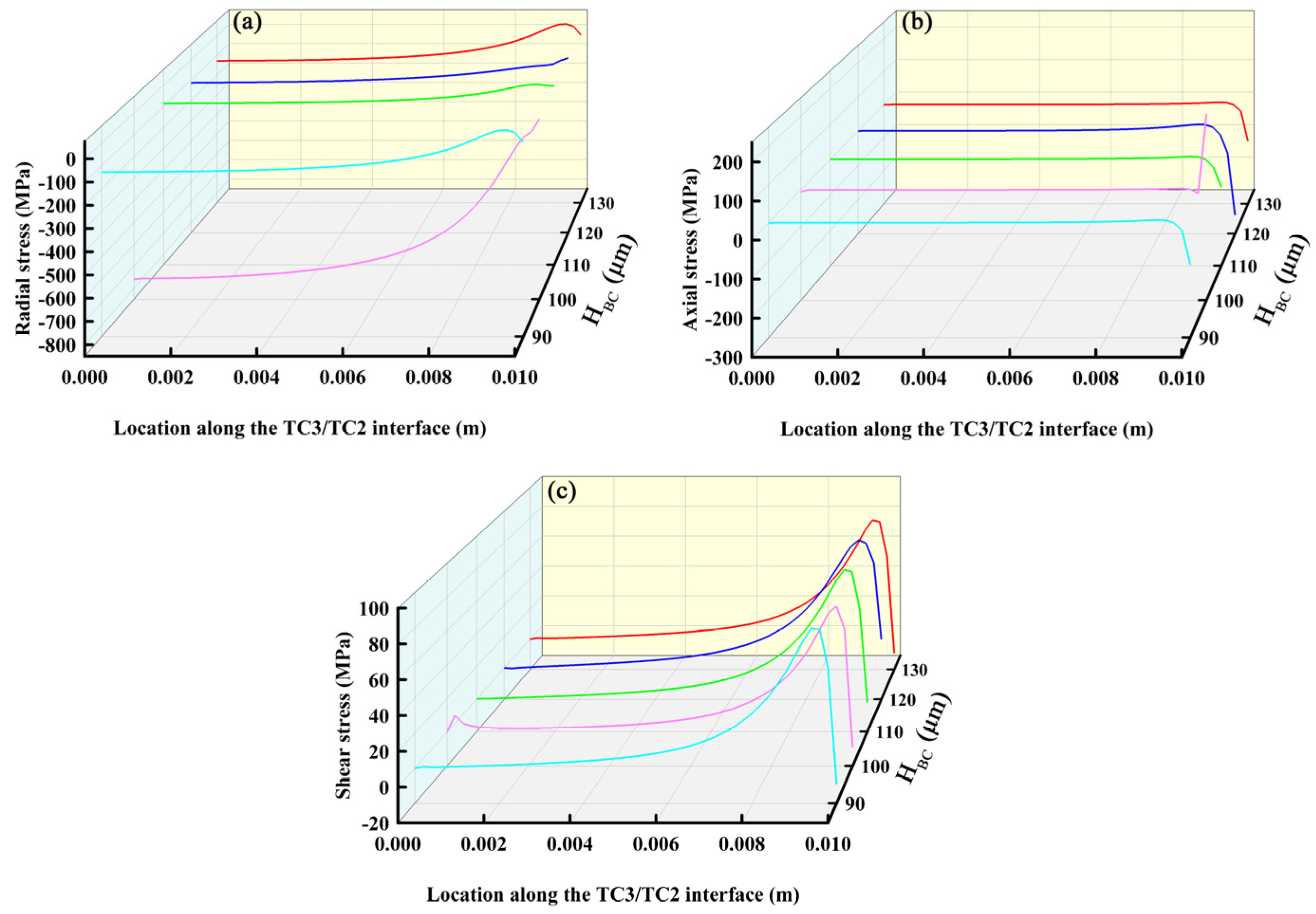
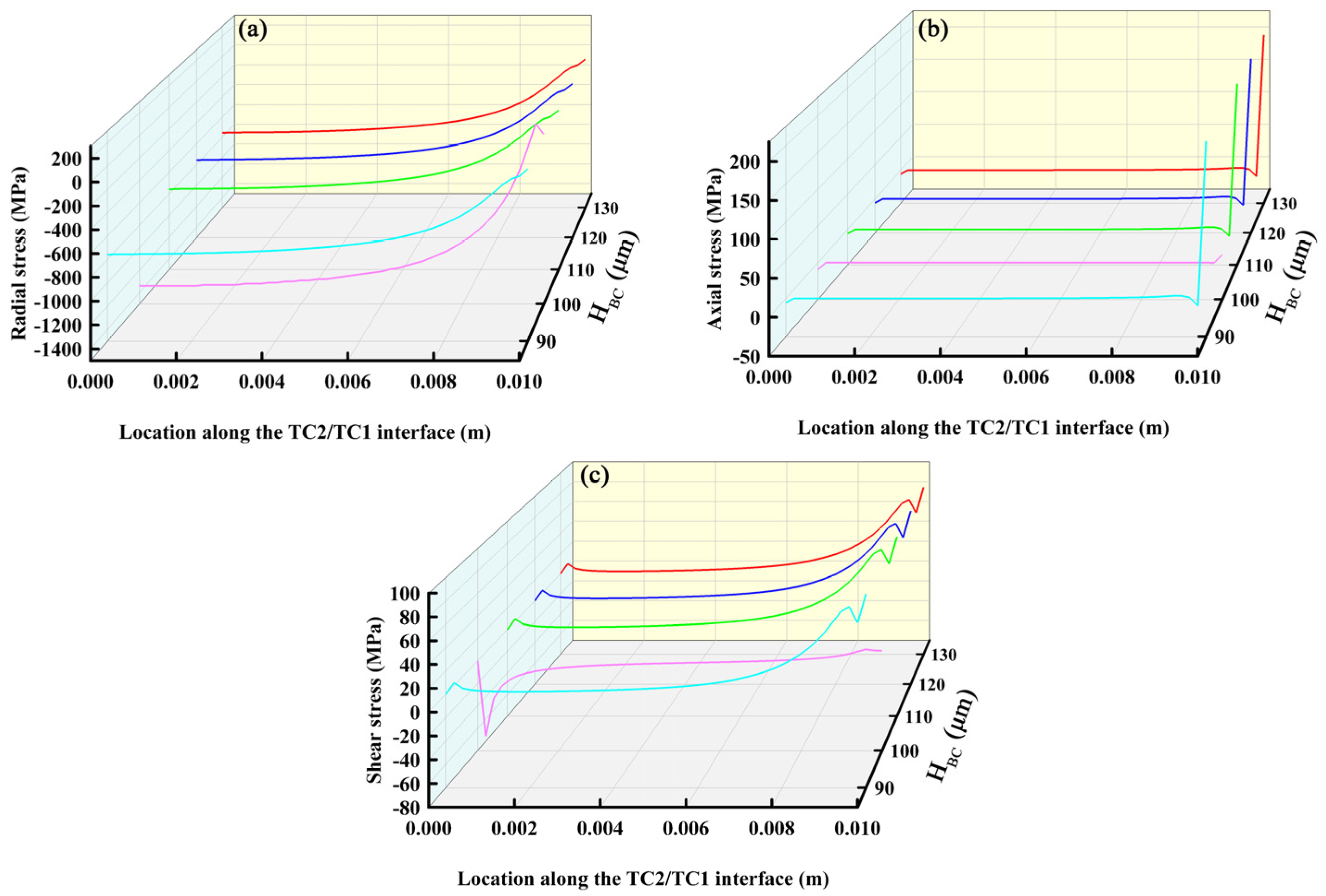
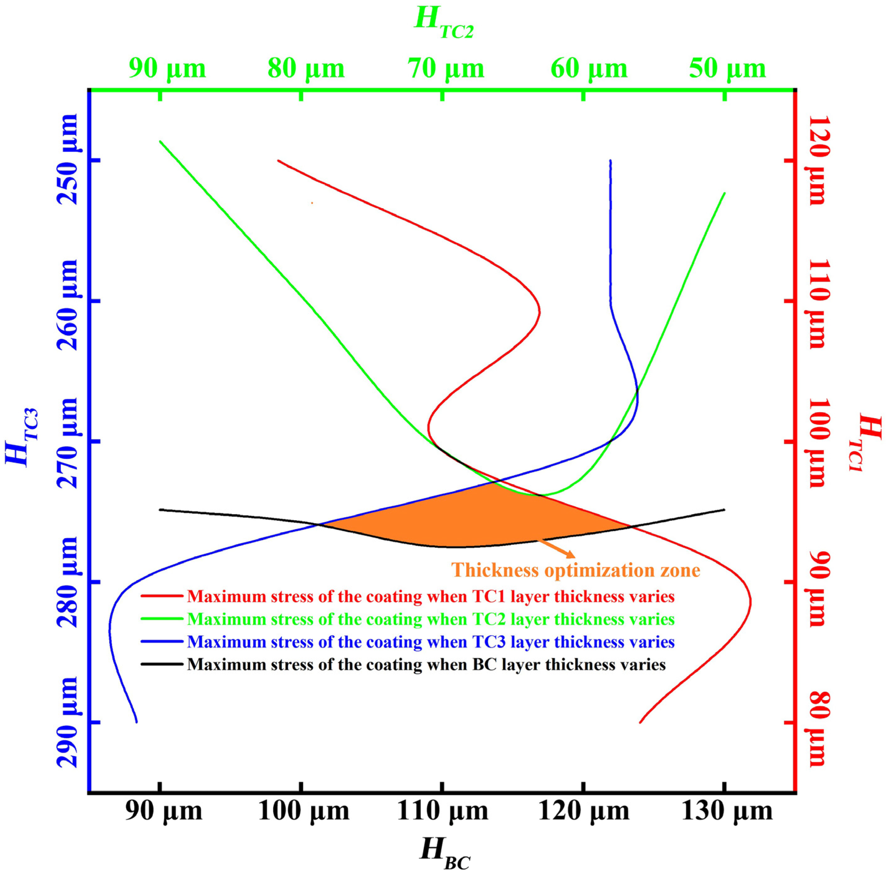
3.1. Influence of Thickness of Each Ceramic Layer on Interfacial Stress

The stress distribution after cooling from high temperature to room temperature over 1800 s after spraying is shown in Figure 4. The tensile stress was positive and the compressive stress was negative. As shown in Figure 4a, the compressive stress primarily existed in the ceramic layer and interface, and tensile stress existed near the substrate layer. The maximum tensile and the maximum compressive stresses were 219 and 1390 MPa, respectively. Figure 4b shows the axial stress distribution nephogram. It can be seen that the maximum axial tensile stress in the ceramic layer was 324 MPa. Figure 4c shows the shear stress distribution map. It can be seen that the tensile and compressive stresses mainly existed in the interior of the coating, and the residual stress was concentrated at the edge of the coating, especially near the interface. Figure 5 shows the failure mechanism of the cooling coating. Because of the different thermal expansion coefficients, when the sprayed sample is cooled, the shrinkage ratio of each layer was different, and a bending moment was formed on the coating, as shown in the diagram. This is equivalent to stretching the outer surface of the coating. Simultaneously, there was a decrease in the tensile stress between the contact surfaces of each layer of the substrate. At this time, the coating can delaminate from the interface of each layer. Therefore, it was important to study the distribution of residual stress of the coating at the interface during thickness optimization.

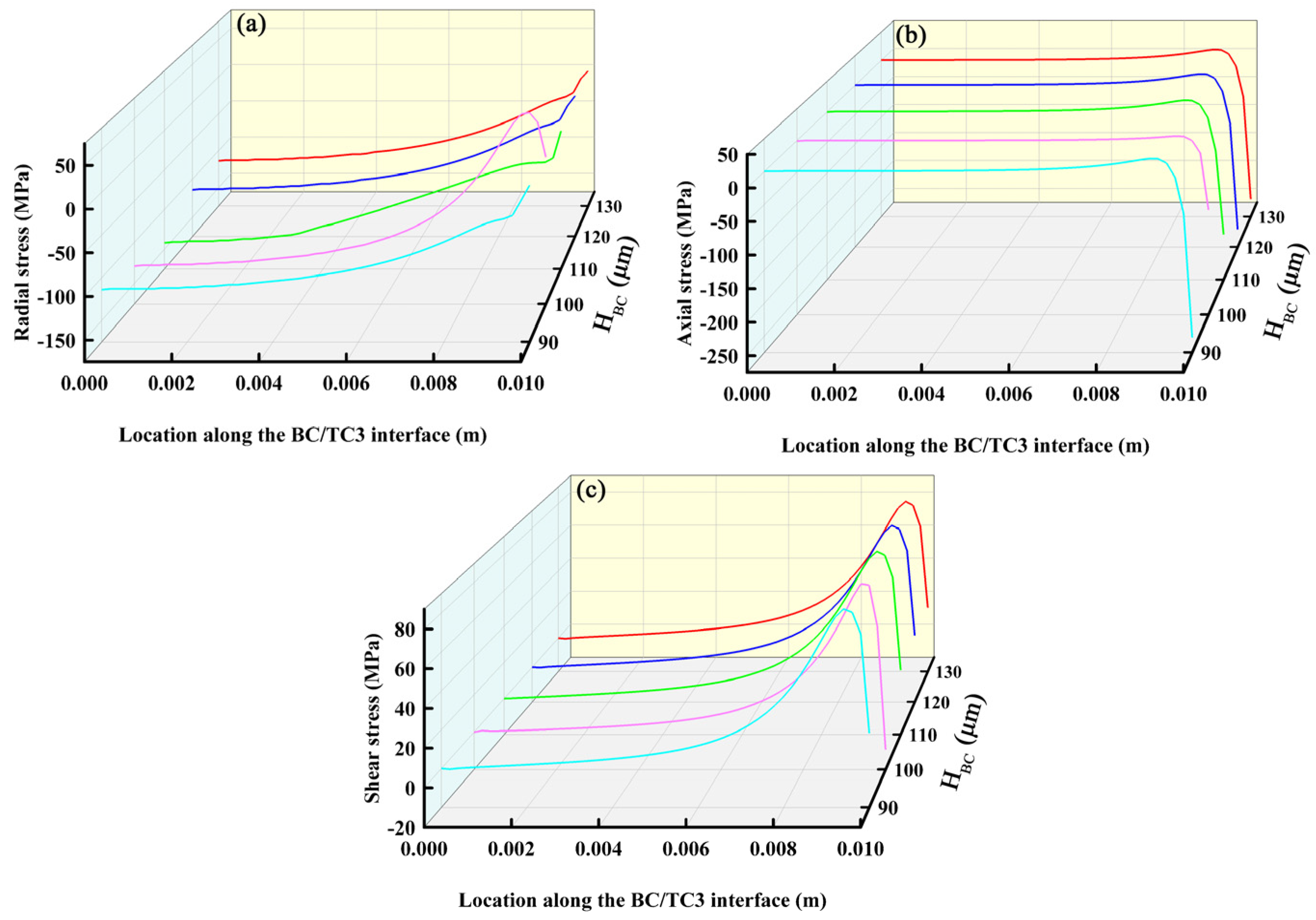
3.1.1. Effect of Bond Layer Thickness on Interfacial Stress

Figure 6, Figure 7, Figure 8 and Figure 9 show the distributions of residual stress at the interfaces of each layer with respect to the thickness of the BC layer (HBC). The data in the figure were obtained by extracting the stress values of the layers along the radial direction. The X axis represents the position of different interfaces in the radial direction, the Y axis represents the change of the thickness of each layer, and the Z axis represents the stress value of each layer interface. Taking Figure 6 as an example, the X axis in Figure 6a represents the position where the radial stress occurs at the SUB/BC interface, the Y axis is the thickness variation of the BC layer, and the Z axis is the radial stress at the SUB/BC interface. Figure 6a shows the distribution curve of the radial stress of the interface between the SUB layer and BC layer with the thickness of the BC layer. Other graphs are the same. In Figure 6, Figure 7, Figure 8 and Figure 9, the stress distribution between different interfaces is extracted when the thickness of the BC layer changes. Currently, the variable only changes the thickness of the BC layer, and the others remain unchanged. Thus, Figure 6 shows the stress distributions at the SUB and BC layer interfaces, while Figure 7 shows that of the BC and TC3 interfaces, Figure 8 shows that of the TC3 and TC2 interfaces, and Figure 9 shows the stress distributions at the TC2 and TC1 interfaces. As shown in Figure 6a, Figure 7a, Figure 8a and Figure 9a, the radial stress gradually decreases as the interface moves from the left side to the right side of the TBCs, and the minimum compressive stress is on the right side of the model. As shown in Figure 6b and Figure 8b, the axial stress changes from the left side of the model to the right side of the model along the interface, and the axial tensile stress changes to compressive stress. However, the axial stress in Figure 9b distinctly increases sharply from the left side of the model to the right side of the model at the edge, which may be because the shrinkage degree of the top layer is larger than that of the bottom three layers during cooling. This shows tensile stress at the edge. The presence of such tensile stresses can cause the coating to delaminate easily and thus cause the coating to fail here. Figure 6c, Figure 7c, Figure 8c and Figure 9c show the contour plots of the interfacial shear stresses caused by the change in the thickness of the BC layer. It can be seen that the residual stress at the interface was redistributed after cooling, resulting in an uneven distribution of tensile stress at the interface. This could lead to delamination and spalling of the coating. Simultaneously, a stress concentration occurred at the edge of the coating interface, followed by a steep decrease in the stress, resulting in crack initiation. The comparisons between Figure 9 and Figure 6 and between Figure 7 and Figure 8 show that when the thickness of the BC layer changes, it has the greatest effect on the interfacial stress distribution pattern of TC1 and TC2 layers, which may be due to the fact that only the top layer performs heat exchange during the simulation, and the thermal expansion coefficient of the top layer is larger such that its thermal stress changes most significantly when the thermal conditions change. We also extracted and analyzed the influence law on the interfacial stresses between the layers when the thickness of the other layers was varied. The influence law derived from the analysis of the other layers is basically the same as the influence of the thickness variation of the bonded layer on the interfacial stresses. Radial and shear stresses in the coating decrease with increasing distance from the center to the edge. Radial and shear stresses decrease with increasing center-to-edge distance, abruptly decreasing at the edges of the specimen, while axial residual stresses increase abruptly at the edge of the substrate. All residual stresses decrease with increases in the coefficient of thermal expansion of the substrate. The thickness of the substrate has an effect on the radial residual stresses, while the axial residual stresses and shear stresses are hardly affected by the thickness of the substrate [57]. A detailed analysis of the thickness variation of the TC3 layer is shown in Figures S1–S4 in Supplementary Materials, a detailed analysis of the thickness variation of the TC2 layer is shown in Figures S5–S8 in Supplementary Materials, and a detailed analysis of the thickness variation of the TC3 layer is shown in Figures S9–S12 in the Supplementary Materials.

3.1.2. Summary of This Section

The thickness of the coating was an important factor that affects residual stress. When the coating was too thin, there was no significant improvement in the thermal insulation effect. However, when the coating was too thick, a large surface residual stress occurred after thermal spraying. If the coating thickness exceeded a certain value, peeling was observed when the coating was cooled from a high temperature to room temperature after thermal spraying.
In order to ensure the best effect of the coating, the thickness of each coating and its maximum stress were optimized, and the design optimization diagram of the stress thickness was obtained, as shown in Figure 10. Figure 10 shows the curve of the maximum stress of the coating with a change of thickness of each layer. The curves in each color represent the maximum stresses as the thickness of the different layers varies. The stress axes are all located on the left side of the respective axes, but since the optimization is conducted to determine the thickness, the axes showing the stress values are hidden, and only the axes showing the thickness are kept for the plot. It can be seen that since the thermal performance parameters of the material of each layer of the coating change with temperature, the maximum stress of the coating after the change of the thickness of each layer presents a non-linear situation, and since it is necessary to ensure that the overall stress level for the use of the coating is not too high, it does not directly select the lowest minimum stress point of each layer. Instead, a reasonable range of thickness optimization is obtained by selecting the location where the stress is lower for each layer thickness change, as shown in the orange area in the figure. Therefore, the thickness of each layer is selected from this region. The thickness optimization range in the figure is based on the theoretical value calculated by the simulation, which is about 95 μm. The thickness of our current spraying process is an integer multiple at each spraying. Therefore, the thickness of the TC1 layer close to the theoretical range is selected as 100 μm. Similarly, the TC3 layer also selects 270 μm instead of 275 μm. Thus, the thicknesses of the BC, TC3, TC2 and TC1 layers are about 110, 270, 70 and 100 μm, respectively.

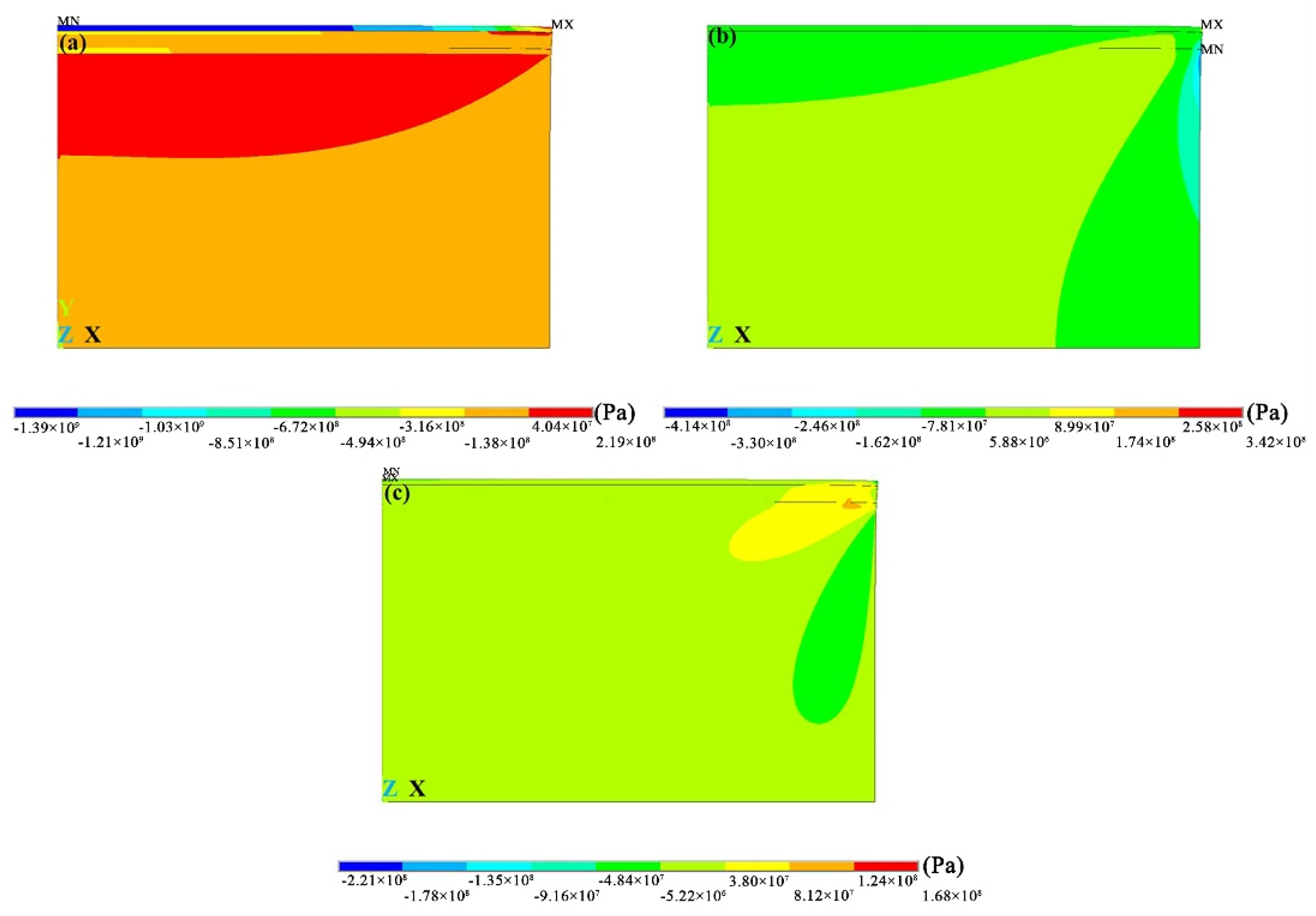
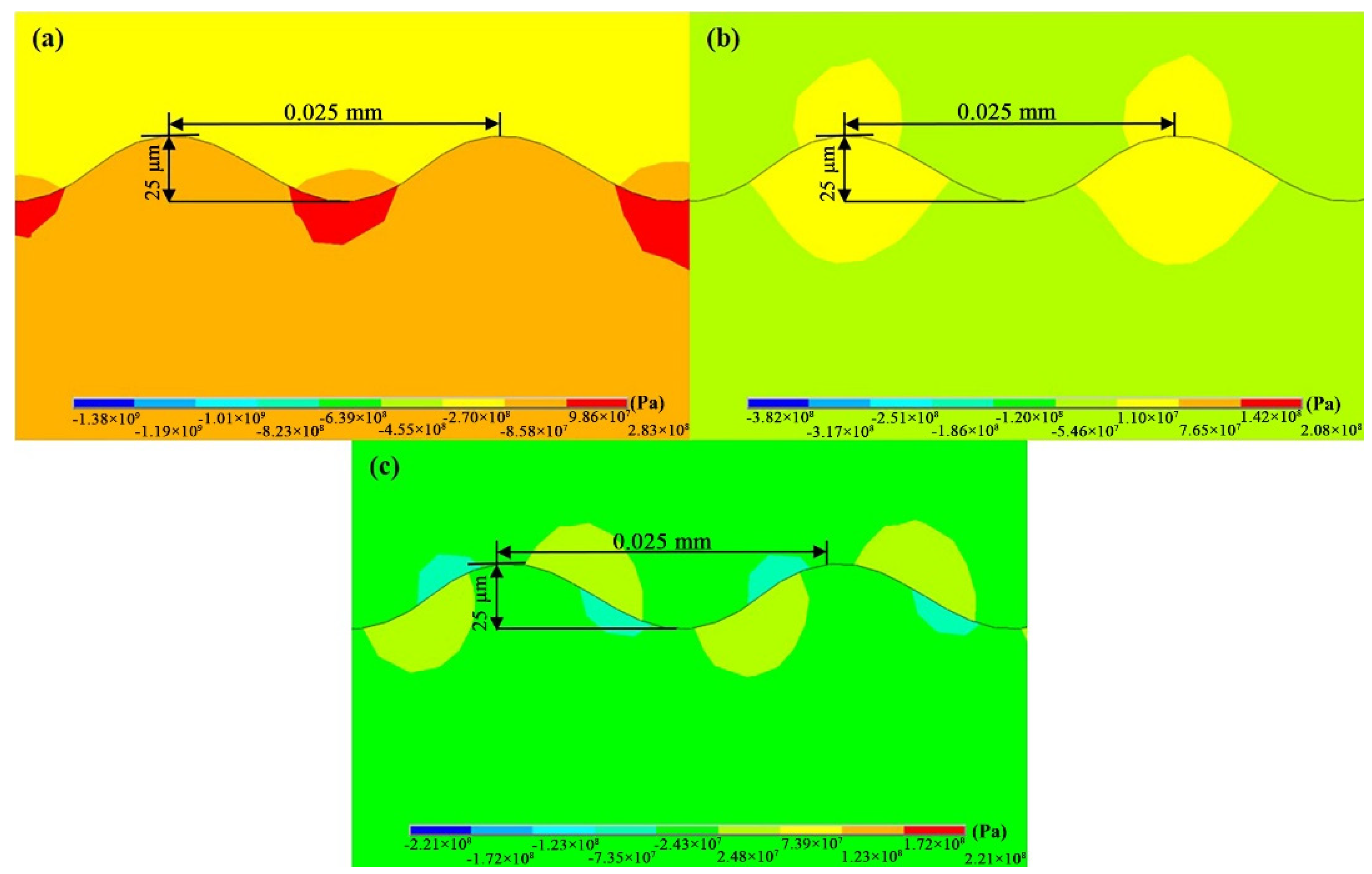
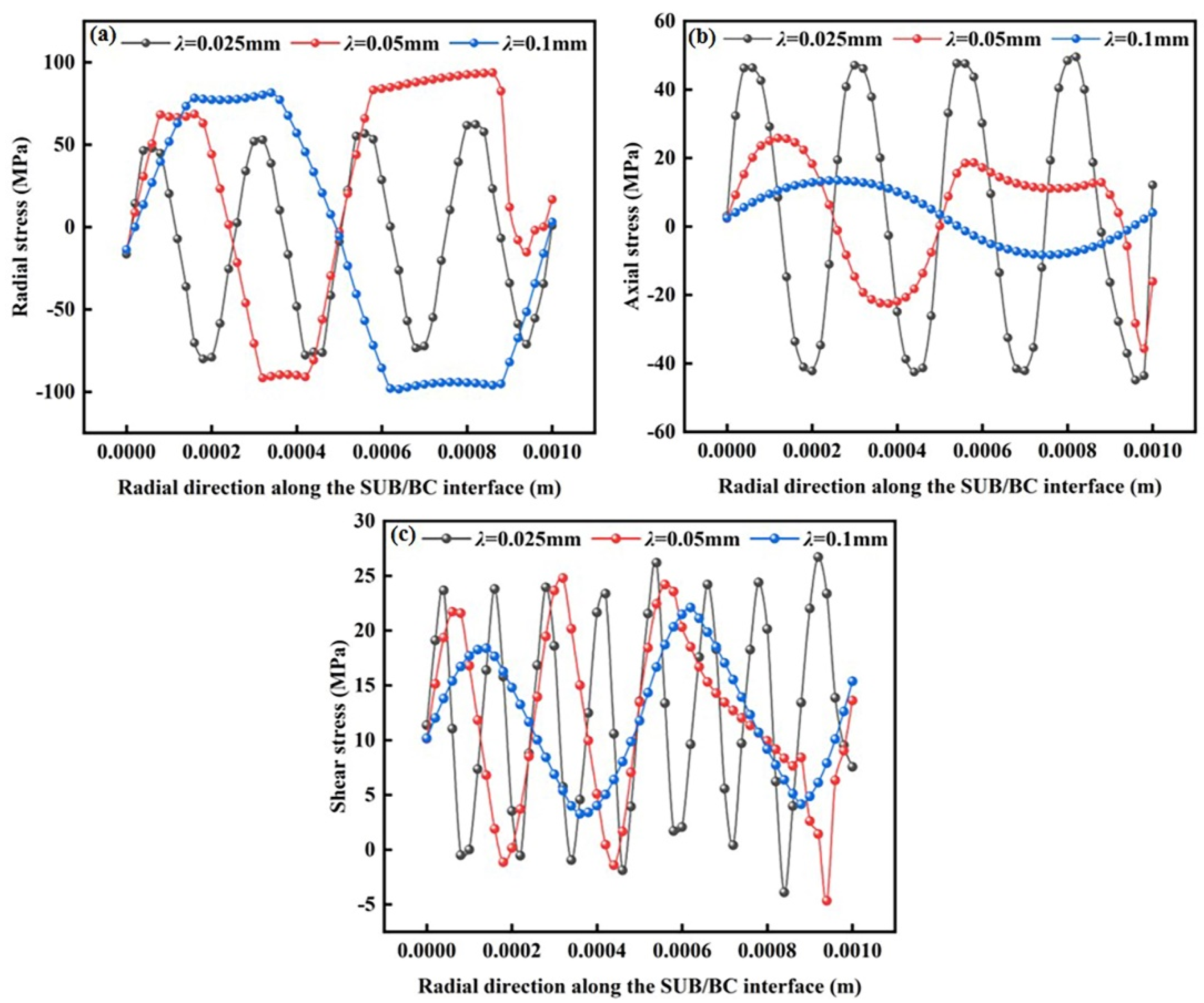
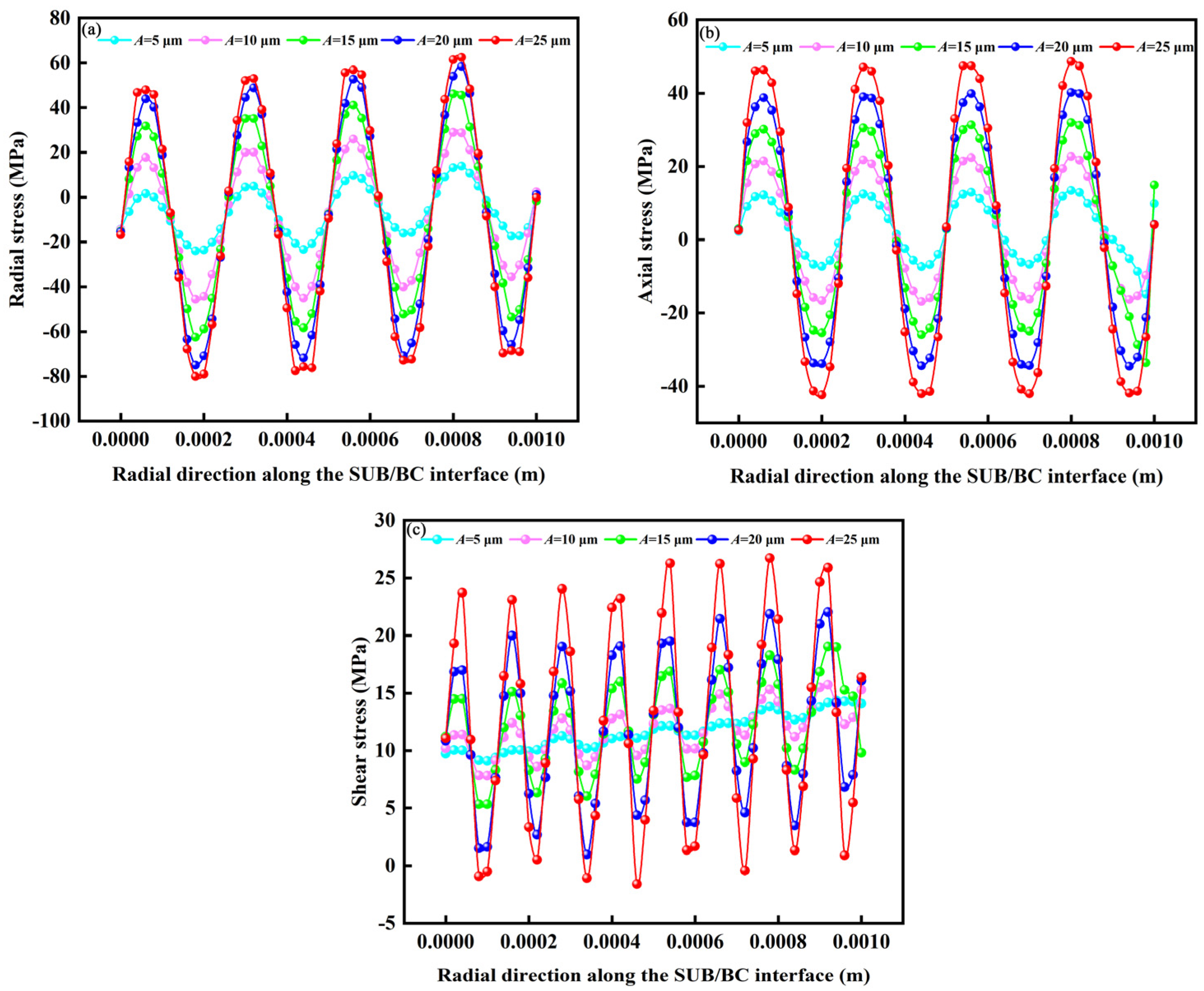
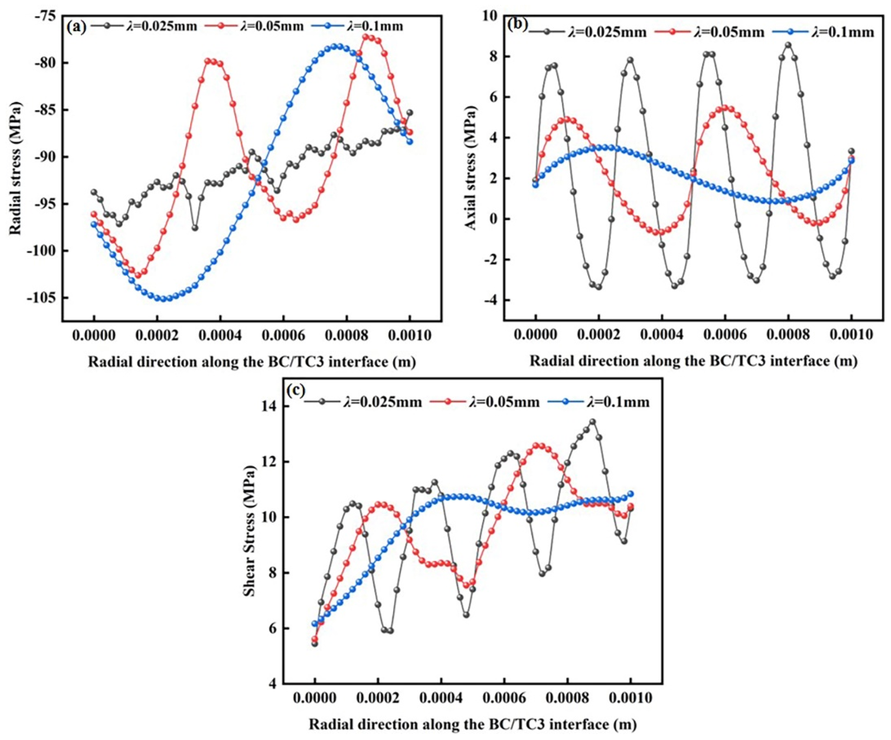
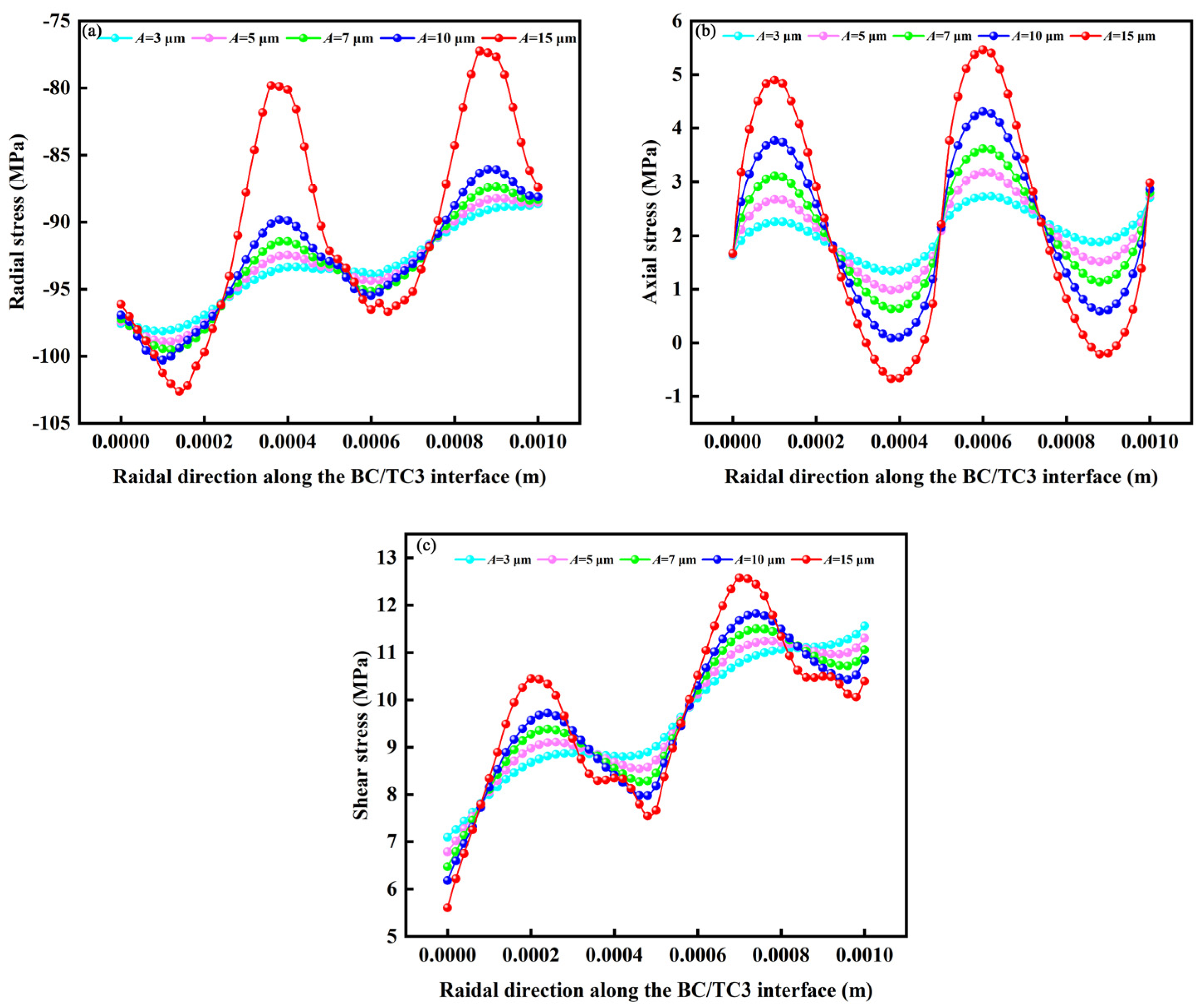
3.2. Influence of Interface Morphology on Interfacial Stress

To simulate the typical surface roughness after plasma spraying, semicircular, sine, and cosine waves are typically used for the geometric shapes of the interface [33,34,48]. In this study, a sine wave was used for the geometry of the interface, and the wavelength and amplitude were determined using the following equations:
y = A sin ( 2 π λ x ) ,
where A is the amplitude, and λ is the wavelength.
Figure 11 shows the stress distribution contour plot of stress of the interface position amplification after the change in the SUB interface structure. Combined with Figure 4, it can be seen that along the sine wave interface, the stress changed with position. The tensile and compressive stresses at the vertical interface of the matrix and bond coat layers appeared at the peaks and valleys of the interface, respectively. The maximum radial tensile stress appeared in the middle of the valley of the interface, and the axial tensile stress appeared in the middle of the valley of the interface. As can be seen from the maximum compressive stress in the figure, the compressive stress decreases significantly with increasing wavelength. This is similar to the results obtained by Han and Hou; they showed that the residual stresses were clearly influenced by the interfacial morphological units. The compressive stresses are present in the depressed morphological units [58,59].

3.2.1. Effect of Interface Morphology of Substrate on Interfacial Stress

Because the interface is simplified by a sine curve, the stress variation law of the coating at the same interface in different periods is basically the same under the same condition. In order to avoid too much repetition, the curve in Figure 12, Figure 13, Figure 14 and Figure 15 is drawn by taking the shape-changing interface stress value within 1 mm at the same position. For example, Figure 12 takes the stress curve of different SUB interface wavelengths in the same position of 1 mm and draws the stress value in this range to obtain a stress diagram as shown in Figure 12. Similarly, Figure 13, Figure 14 and Figure 15 are the same. Figure 12 shows the stress changes at the interface of the substrate and bond-coat layers for different wavelengths within the same distance range. Figure 12a shows the radial stress distribution map of the SUB/BC interface under different wavelength changes. A decrease in wavelength decreased the interfacial stress, indicating that under the same amplitude, a larger wavelength results in a smoother interface with less reduction in the interfacial stress. Figure 12b shows the distribution of axial stress at the SUB/BC interface at different wavelengths. The compressive stress was concentrated near the bottom of the trough, and the tensile stress was concentrated at the peak. When the tensile stress exceeded the bonding strength in this region, the coating was prone to delamination failure. Figure 12c shows the distribution of shear stress along the SUB/BC interface. The tensile stress at the interface trough increased with an increase in the wavelength. This resulted in the initiation of cracks owing to large tensile stress, accelerating the propagation of interface cracks, and causing the microcracks to become long cracks.
Figure 13 shows the stress changes at the interface between the substrate and bond-coat layers at different amplitudes under the same cycle. Figure 13a shows the distribution of the radial stress along the SUB/BC interface under different amplitudes. As shown in Figure 13b, the axial tensile stress of the TBCs was concentrated at the peak of the interface, and the compressive stress was concentrated at the valley of the interface. Figure 13c displays the distribution of shear stress. The interfacial tensile stress increased with amplitude, and the maximum tensile stress appeared outside the interface wave crest. A smaller amplitude led to a smoother interface. There was a minor compressive stress near the interface valley and a tensile stress concentration at the interface peak.

3.2.2. Effect of Interface Morphology of Bond Layer on Interfacial Stress

Figure 14 shows the variation in stress in the BC layer interface structure at different wavelengths within the same distance, where a longer wavelength resulted in a smaller residual stress. The smaller the wavelength, the greater the compressive stress parallel to the interface, the greater the curvature of the interface, and the rougher the interface. It follows that the compressive stress parallel to the interface increases as the curvature of the interface increases, which is the same law as the effect of the change in wavelength of the BC interface of the coating on the interface stress. Therefore, when designing the interface of thermal barrier coating, we should try to avoid the appearance of rougher interface morphology.
Figure 15 shows the stress changes in the interface structure of the BC layer under different amplitudes at the same distance. As shown in Figure 15, the change in radial stress is periodic when the amplitude changes, and the maximum tensile and compressive stresses appear at the interface peak and trough, respectively. It can be seen that as the amplitude increases, the stress at the interface increases, and the effect on tensile stress is much greater than the effect on compressive stress, indicating that the coating is prone to delamination failure. This is due to the increase in amplitude, which leads to roughness of the interface, and the interface stress increases with the increase in the roughness of the interface. The greater the amplitude, the greater the residual stress, indicating that a rough interface causes a larger residual stress.

3.2.3. Summary of This Section
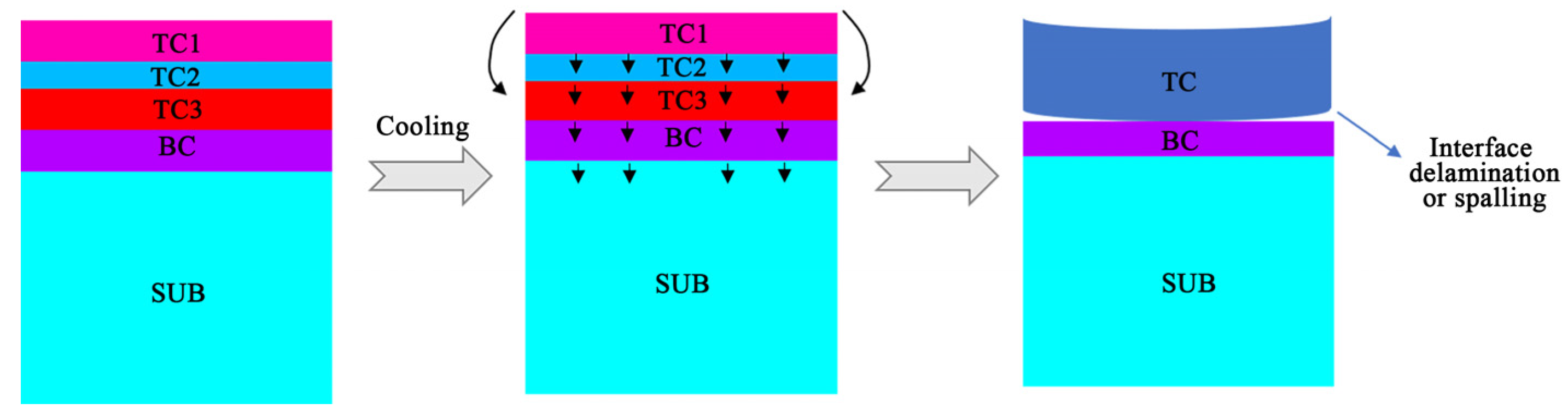
This study of the atmospheric plasma spraying (APS) process as well as the substrate by sandblasting after spraying appears with high roughness. The cooling stress of the coating after spraying is not in service under high temperature conditions; thus, the effect of TGO is basically negligible. At this time, the sine curve can be used to optimize the interface without considering the influence of the TGO layer. Simulations of the interfacial structure of the coating substrate and the bonded coating indicate that a rough interface can effectively relieve stress concentrations, supposedly because the change in interfacial roughness alters the residual stresses in the coating system due to thermal strain mismatch. If the interface becomes rougher, tensile stresses may be concentrated in the region near the peak of the interface, suggesting that initial cracking is more likely to occur near the peak region of the rougher interface. Based on the variation of normal stresses with different roughness parameters, it can be concluded that if the interface becomes rougher, the near-peak region is more prone to cracking, and then, further cracking and eventual spalling of the ceramic layer starts to occur from there. As the wavelength of SUB and BC layers become larger and the amplitude becomes smaller, the residual stress gradually becomes smaller, which also verifies that a smooth surface is beneficial to reduce the residual stress level at the interface, while a rough interface avoids excessive local compressive stress at the interface, which also provides insight into the processing and control of the interface microstructure.

4. Conclusions

An Al2O3-YAG/ZrO1.5-YO1.5-TaO1.5/8YSZ/NiCoCrAlY multilayer ceramic top coating prepared by plasma spraying was simulated using the FEM. The simulations were carried out mainly for multilayer coatings in the sprayed state, without considering the effect of TGO formed during the high-temperature oxidation process. The following conclusions apply only to the case of minimizing failures caused by the thermo-mechanical effects (CTE mismatch):
  • Based on the influence of the thickness optimization of each layer on the stress distributions of each interface, it can be concluded that to ensure that the residual stress of the coating is small and that it has good thermal insulation performance, the thicknesses of the BC, TC3, TC2, and TC1 layers should be approximately 110, 270, 70, and 100 μm, respectively. The thickness ratio was approximately 11:27:7:10.
  • A periodic sine function was constructed to simulate the interface morphology of the coating during the plasma spraying. Based on the influence of a change in the interface morphology on the distributions of the interfacial stress, a relatively smooth interface could effectively reduce the concentration of the interfacial residual stress.

Supplementary Materials

The following supporting information can be downloaded at: https://www.mdpi.com/article/10.3390/coatings12111660/s1, Figure S1: Stress distribution along the SUB/BC interface when the thickness of TC3 layer varies: (a) radial stress; (b) axial stress and (c) shear stress.; Figure S2: Stress distribution along the BC/TC3 interface when the thickness of TC3 layer varies: (a) radial stress; (b) axial stress and (c) shear stress; Figure S3: Stress distribution along the TC3/TC2 interface when the thickness of TC3 layer varies: (a) radial stress; (b) axial stress and (c) shear stress; Figure S4: Stress distribution along the TC2/TC1 interface when the thickness of TC3 layer varies: (a) radial stress; (b) axial stress and (c) shear stress; Figure S5: Stress distribution along the SUB/BC interface when the thickness of TC2 layer varies: (a) radial stress; (b) axial stress and (c) shear stress; Figure S6: Stress distribution along the BC/TC3 interface when the thickness of TC2 layer varies: (a) radial stress; (b) axial stress and (c) shear stress; Figure S7: Stress distribution along the TC3/TC2 interface when the thickness of TC2 layer varies: (a) radial stress; (b) axial stress and (c) shear stress; Figure S8: Stress distribution along the TC2/TC1 interface when the thickness of TC2 layer varies: (a) radial stress; (b) axial stress and (c) shear stress; Figure S9: Stress distribution along the SUB/BC interface when the thickness of TC1 layer varies: (a) radial stress; (b) axial stress and (c) shear stress; Figure S10: Stress distribution along the BC/TC3 interface when the thickness of TC1 layer varies: (a) radial stress; (b) axial stress and (c) shear stress; Figure S11: Stress distribution along the TC3/TC2 interface when the thickness of TC1 layer varies: (a) radial stress; (b) axial stress and (c) shear stress; Figure S12: Stress distribution along the TC2/TC1 interface when the thickness of TC1 layer varies: (a) radial stress; (b) axial stress and (c) shear stress.

Author Contributions

Conceptualization, H.-X.Z. and L.W.; methodology, H.-Y.S. and L.W.; software, H.-Y.S., Y.L. and Z.-J.C.; validation, H.-Y.S., X.-W.S. and J.-B.W.; formal analysis, H.-Y.S.; investigation, H.-Y.S.; resources, L.W.; data curation, H.-Y.S., Q.W. and J.-H.S.; writing—original draft preparation, H.-Y.S.; writing—review and editing, L.W.; visualization, H.-Y.S.; supervision, H.-Y.S.; project administration, L.W.; funding acquisition, L.W. All authors have read and agreed to the published version of the manuscript.

Funding

This research was supported by the sub-projects of the Key Basic Research Projects of Basic Strengthening Program (grant no. 2020-JCJQ-ZD-172-05), Basic Research (grant no. JCKY2021603B007), Training Program of the Major Research Plan of the National Natural Science Foundation of China (no. 91960107), the financial support of the National Natural Science Foundation of China (no. 51671208, no. 52001180), National NSAF (grant no. U1730139). Youth Innovation Promotion Association of the Chinese Academy of Sciences (grant no. 2017295), and the Natural Science Foundation of Shanghai (no. 19ZR1479600).

Institutional Review Board Statement

Not applicable.

Informed Consent Statement

Not applicable.

Data Availability Statement

Not applicable.

Conflicts of Interest

The authors declare no conflict of interest.

References

  1. Thakare, J.G. Thermal Barrier Coatings—A State of the Art Review. Met. Mater. Int. 2021, 27, 1947–1968. [Google Scholar] [CrossRef]
  2. Kanwal, S.; Thakare, J.G.; Pandey, C.; Singh, I.; Mahapatra, M.M. Characterization of slurry-based mullite coating deposited on P91 steel welds. J. Aust. Ceram. Soc. 2019, 55, 519–528. [Google Scholar] [CrossRef]
  3. Padture, N.P.; Gell, M.; Jordan, E.H. Thermal barrier coatings for gas-turbine engine applications. Science 2002, 296, 280–284. [Google Scholar] [CrossRef] [PubMed]
  4. Ming, Y.; Yuhua, L.; Ming, L. Research review of thermal barrier coatings preparation methods. J. Hubei Polytech. Univ. 2021, 37, 33–38. [Google Scholar] [CrossRef]
  5. Mercer, C. On a ferroelastic mechanism governing the toughness of metastable tetragonal-prime (t′) yttria-stabilized zirconia. Proc. R. Soc. A 2007, 463, 1393–1408. [Google Scholar] [CrossRef]
  6. Zhao, M.; Pan, W. Effect of lattice defects on thermal conductivity of Ti-doped, Y2O3-stabilized ZrO2. Acta Mater. 2013, 61, 5496–5503. [Google Scholar] [CrossRef]
  7. Zhao, M.; Ren, X.; Yang, J.; Pan, W. Thermo-mechanical properties of ThO2-doped Y2O3 stabilized ZrO2 for thermal barrier coatings. Ceram. Int. 2016, 42, 501–508. [Google Scholar] [CrossRef]
  8. Schelling, P.K. Mechanism of the cubic-to-tetragonal phase transition in zirconia and yttria-stabilized zirconia. J. Am. Ceram. 2001, 84, 2997–3007. [Google Scholar] [CrossRef]
  9. Fengling, L. The structure design of thermal barrier coating for 21 century. Mater. Prot. 2000, 33, 86–88. [Google Scholar] [CrossRef]
  10. Clarke, D.R.; Levi, C.G. Materials design for the next generation thermal battier coatings. Annu. Rev. Mater. Res. 2003, 33, 383–417. [Google Scholar] [CrossRef]
  11. Thakarea, J.G. Mechanical property evaluation of carbon nanotubes reinforced plasma sprayed YSZ-alumina composite coating. Ceram. Int. 2018, 44, 6980–6989. [Google Scholar] [CrossRef]
  12. Kim, D.J.; Tien, T.Y. Phase stability and physical properties of cubic and tetragonal ZrO2 in the system ZrO2–Y2O3–Ta2O5. J. Am. Ceram. Soc. 1991, 74, 3061–3065. [Google Scholar] [CrossRef]
  13. Pitek, F.M.; Levi, C.G. Opportunities for TBCs in the ZrO2-YO1.5-TaO2.5 system. Surf. Coat. Technol. 2007, 201, 6044–6050. [Google Scholar] [CrossRef]
  14. Shian, S. The tetragonal–monoclinic, ferroelastic transformation in yttrium tantalate and effect of zirconia alloying. Acta Mater. 2014, 69, 196–202. [Google Scholar] [CrossRef]
  15. Wu, J.; Wei, X.; Padture, N.P. Low-thermal-conductivity rare-earth zirconates for potential thermal-barrier-coating applications. J. Am. Ceram. Soc. 2002, 85, 3031–3035. [Google Scholar] [CrossRef]
  16. Lin, C.; Jing, F. Research progress on thermal mechanical properties of rare earth tantalate RE3TaO7 and RE3TaO9 ceramics. Mod. Tech. Ceram. 2019, 40, 31. [Google Scholar] [CrossRef]
  17. Muller, J.; Schierling, M. Chemical vapor deposition of smooth α-Al2O3 films on nickel base superalloys as diffusion barriers. Surf. Coat. Technol. 1999, 120, 16–21. [Google Scholar] [CrossRef]
  18. Pint, B.A. High-temperature oxidation-resistant alloys: Recent developments in science and applications. JOM 2009, 61, 42–43. [Google Scholar] [CrossRef]
  19. Ren, C.; He, Y.; Wang, D. High-temperature cyclic oxidation behavior of Al2O3-YAG composite coating prepared by EPD and microwave sintering. Appl. Surf. Sci. 2012, 258, 5739–5745. [Google Scholar] [CrossRef]
  20. Pereira, P.F.S. Red, green and blue (RGB) emission doped Y3Al5O12 (YAG) phosphors prepared by non-hydrolytic sol–gel route. J. Lumin. 2010, 130, 488–493. [Google Scholar] [CrossRef]
  21. Zheyi, Z. Study on process optimization of sprayable powders and deposition performance of amorphous Al2O3–YAG coatings. Coatings 2020, 10, 1158. [Google Scholar] [CrossRef]
  22. Yang, K.; Rong, J.; Feng, J. In-situ fabrication of amorphous/eutectic Al2O3-YAG ceramic composite coating via atmospheric plasma spraying. J. Eur. Ceram. Soc. 2016, 36, 4261–4267. [Google Scholar] [CrossRef]
  23. Parthasarathy, T.A.; Mah, T.I.; Keller, K. Creep mechanism of polycrystalline yttrium aluminum garnet. J. Am. Ceram. Soc. 1992, 75, 1756–1759. [Google Scholar] [CrossRef]
  24. Waku, Y.; Ohtsubo, H.; Nakagawa, N. Sapphire matrix composites reinforced with single crystal YAG phases. J. Mater. Sci. 1996, 31, 4663–4670. [Google Scholar] [CrossRef]
  25. Ochiai, S.; Ueda, T.; Sato, K. Deformation and fracture behavior of an Al2O3/YAG composite from room temperature to 2023 K. Compos. Sci. Technol. 2001, 61, 2117–2128. [Google Scholar] [CrossRef]
  26. Miyazaki, N.; Ikeda, T.; Komura, T. Estimation of steady-state creep behavior of Al2O3/YAG eutectic composite by image-based finite element analysis. J. Eng. Mater. Technol. 2003, 125, 277–282. [Google Scholar] [CrossRef]
  27. Sommer, F.; Kern, F.; El-Maghraby, F.H. Effect of preparation route on the properties of slip-casted Al2O3/YAG composites. Ceram. Int. 2012, 38, 4819–4826. [Google Scholar] [CrossRef]
  28. Lim, G.; Kar, A. Radiative properties of thermal barrier coatings at high temperatures. J. Phys. D Appl. Phys. 2009, 42, 155412. [Google Scholar] [CrossRef]
  29. Lee, G.; Atkinson, A.; Selçuk, A. Development of residual stress and damage in thermal barrier coatings. Surf. Coat. Technol. 2006, 201, 3931–3936. [Google Scholar] [CrossRef]
  30. Mao, W.G.; Zhou, Y.C.; Yang, L. Modeling of residual stresses variation with thermal cycling in thermal barrier coatings. Mech. Mater. 2006, 38, 1118–1127. [Google Scholar] [CrossRef]
  31. Faruk, S. Stress analysis of high temperature ZrO2 insulation coatings on Ag using finite element method. J. Mater. Process. Technol. 2006, 180, 239–245. [Google Scholar] [CrossRef]
  32. Ranjbar-Far, M. Impact of the non-homogenous temperature distribution and the coatings process modeling on the thermal barrier coatings system. Mater. Des. 2011, 32, 728–735. [Google Scholar] [CrossRef]
  33. Ozkan, S.; Yasar, I.; Erdal, C. Finite element modeling of the effect of the ceramic coatings on heat transfer characteristics in thermal barrier applications. Mater. Des. 2005, 26, 357–362. [Google Scholar] [CrossRef]
  34. Rätzer-Scheibe, H.J.; Schulz, U.; Krell, T. The effect of coating thickness on the thermal conductivity of EB-PVD PYSZ thermal barrier coatings. Surf. Coat. Technol. 2006, 200, 5636–5644. [Google Scholar] [CrossRef]
  35. Guo, H.B.; Vaßen, R.; Stöver, D. Atmospheric plasma sprayed thick thermal barrier coatings with high segmentation crack density. Surf. Coat. Technol. 2004, 186, 353–363. [Google Scholar] [CrossRef]
  36. Ranjbar-Far, M. Simulation of the effect of material properties and interface roughness on the stress distribution in thermal barrier coatings using finite element method. Mater. Des. 2010, 31, 772–781. [Google Scholar] [CrossRef]
  37. Białas, M. Finite element analysis of stress distribution in thermal barrier coatings. Surf. Coat. Technol. 2008, 202, 6002–6010. [Google Scholar] [CrossRef]
  38. Han, M.; Huang, J.; Chen, S. The influence of interface morphology on the stress distribution in double-ceramic-layer thermal barrier coatings. Ceram. Int. 2015, 41, 4312–4325. [Google Scholar] [CrossRef]
  39. Ahrens, M.; Vaßen, R.; Stöver, D. Stress distributions in plasma-sprayed thermal barrier coatings as a function of interface roughness and oxide scale thickness. Surf. Coat. Technol. 2002, 161, 26–35. [Google Scholar] [CrossRef]
  40. Zhang, W.X.; Fan, X.L.; Wang, T.J. The surface cracking behavior in air plasma sprayed thermal barrier coating system incorporating interface roughness effect. Appl. Surf. Sci. 2011, 258, 811–817. [Google Scholar] [CrossRef]
  41. Zhang, D. Effect of bond coat surface roughness on the thermal cyclic behavior of thermal barrier coatings. Surf. Coat. Technol. 2006, 201, 649–653. [Google Scholar] [CrossRef]
  42. Han, M. A parametric study of the double-ceramic-layer thermal barrier coatings part I: Optimization design of the ceramic layer thickness ratio based on the finite element analysis of thermal insulation (take LZ7C3/8YSZ/NiCoAlY DCL-TBCs for an example). Surf. Coat. Technol. 2013, 236, 500–509. [Google Scholar] [CrossRef]
  43. Zhuang, M.X. Design and optimization of coating structure for plasma sprayed self-healing MgO coating via finite element method. Ceram. Int. 2021, 47, 2414–2429. [Google Scholar] [CrossRef]
  44. Wu, Q.; Dong, Y.F.; Wang, Z.; Song, D.Y.; Ji, Y.X. Computational modal analysis of circular saw blade based on APDL method. For. Mach. Woodwork. Equip. 2022, 50, 97–105. [Google Scholar] [CrossRef]
  45. Han, M. Optimization selection of the thermal conductivity of the top ceramic layer in the Double-Ceramic-Layer Thermal Barrier Coatings based on the finite element analysis of thermal insulation. Surf. Coat. Technol. 2014, 240, 320–326. [Google Scholar] [CrossRef]
  46. Lou, S.Y.; Shan, X.; Zhao, X.F. Composition and thickness optimization of anti-CMAS layer on air plasma sprayed thermal barrier coatings. Surf. Coat. Technol. 2018, 47, 208–217. [Google Scholar] [CrossRef]
  47. Han, M.; Huang, J.H.; Chen, S.H. Behavior and mechanism of the stress buffer effect of the inside ceramic layer to the top ceramic layer in a double-ceramic-layer thermal barrier coating. Ceram. Int. 2014, 40, 2901–2914. [Google Scholar] [CrossRef]
  48. Zhou, C.G.; Wang, C.L.; Song, Y.X. Evaluation of cyclic oxidation of thermal barrier coatings exposed to NaCl vapor by finite element method. Mater. Sci. Eng. A 2008, 490, 351–358. [Google Scholar] [CrossRef]
  49. Zhou, C.G. Cyclic-oxidation behavior of thermal-barrier coatings exposed to NaCl vapor. Oxid. Met. 2008, 69, 119–130. [Google Scholar] [CrossRef]
  50. Zhou, C.G. Influence of service temperature on grain growth and thermal diffusivity of nanostructured thermal barrier coating. Mater. Sci. Forum. 2005, 510, 3985–3988. [Google Scholar] [CrossRef]
  51. Han, M.; Huang, J.H.; Chen, S.H. A parametric study of the Double- Ceramic-Layer Thermal Barrier Coating Part II: Optimization selection of mechanical parameters of the inside ceramic layer based on the effect on the stress distribution. Surf. Coat. Technol. 2014, 238, 93–117. [Google Scholar] [CrossRef]
  52. Wang, L. Finite element simulation of stress distribution and development in 8YSZ and double-ceramic-layer La2Zr2O7/8YSZ thermal barrier coatings during thermal shock. Appl. Surf. Sci. 2012, 258, 3540–3551. [Google Scholar] [CrossRef]
  53. Ren, C.; He, Y.D.; Wang, D.R. Cyclic oxidation behavior and thermal barrier effect of YSZ-(Al2O3/YAG) double-layer TBCs prepared by the composite sol–gel method. Surf. Coat. Technol. 2011, 206, 1461–1468. [Google Scholar] [CrossRef]
  54. Hsuch, C.H.; Jong, H.; Lee, C.S. Modeling of thermal stresses in joining two layers with multi- and graded interlayers. J. Am. Ceram. Soc. 2006, 9, 251–257. [Google Scholar] [CrossRef]
  55. Gao, X.Y. Study of residual stresses and stability of thermal barrier coatings under thermal cycling. N. P. U. 2007, 6, 77–79. [Google Scholar] [CrossRef]
  56. Liu, D.D. Research and numerical simulation of thermal of thermal mechanical behavior of thermal barrier coating micromorphology. Southwest Jiaotong Univ. 2018. [Google Scholar]
  57. Zhang, H.S.; Zhang, Z.; Chen, X.G.; Liu, J.Y. Plasma spraying Sm2Zr2O7 Residual thermal stress in thermal barrier coatings. China’s Ceram. 2010, 46, 38–41. [Google Scholar] [CrossRef]
  58. Han, Z.Y.; Wang, H. Relation between concave cone 3 dimension topography and residual stress in thermal barrier coatings. Adv. Mat. Res. 2011, 291, 172–175. [Google Scholar] [CrossRef]
  59. Hou, P.J.; Wang, H.G.; Zha, B.L.; Yuan, X.J. Numerical simulation for effect of interface roughness on residual stress of double-layer thermal barrier coatings. Hot Work. Technol. 2007, 36, 82–85. [Google Scholar]
Figure 1. Schematic illustration of thermal barrier coatings.
Coatings 12 01660 g001
Figure 2. Numerical models: (a) simple physical model; (b) finite element model and mesh and (c) local magnification of model 2b.
Coatings 12 01660 g002
Figure 3. Numerical model: (a) finite element model; (b) enlarged view of the local mesh of model 3a.
Coatings 12 01660 g003
Figure 4. Contour plot of the residual stress when the coating was cooled to room temperature from high temperature: (a) radial stress; (b) axial stress and (c) shear stress.
Coatings 12 01660 g004
Figure 5. Failure mechanism of the coating when cooling to room temperature.
Coatings 12 01660 g005
Figure 6. Stress distributions along SUB/BC interface: (a) radial stress; (b) axial stress and (c) shear stress.
Coatings 12 01660 g006
Figure 7. Stress distributions along BC/TC3 interface: (a) radial stress; (b) axial stress and (c) shear stress.
Coatings 12 01660 g007
Figure 8. Stress distributions along TC3/TC2 interface: (a) radial stress; (b) axial stress and (c) shear stress.
Coatings 12 01660 g008
Figure 9. Stress distributions along TC2/TC1 interface: (a) radial stress; (b) axial stress and (c) shear stress.
Coatings 12 01660 g009
Figure 10. Schematic illustration for thickness design optimization.
Coatings 12 01660 g010
Figure 11. Distribution at the interface with the sine wave morphology: (a) radial stress; (b) axial stress and (c) shear stress.
Coatings 12 01660 g011
Figure 12. Stress distributions of SUB/BC interface at different wavelengths: (a) radial stress; (b) axial stress and (c) shear stress.
Coatings 12 01660 g012
Figure 13. Stress distributions of SUB/BC interface at different amplitudes: (a) radial stress; (b) axial stress and (c) shear stress.
Coatings 12 01660 g013
Figure 14. Stress distributions of BC/TC3 interface at different wavelengths: (a) radial stress; (b) axial stress and (c) shear stress.
Coatings 12 01660 g014
Figure 15. Stress distributions of BC/TC3 layer interface at different amplitudes: (a) radial stress; (b) axial stress and (c) shear stress.
Coatings 12 01660 g015
Table 1. Material parameters of GH3128 for SUB layer [48,49,50,51].
T (°C)E (GPa)vα (×10−6 °C−1)kc (J/(Kg·°C))ρ (kg/m3)
202200.3114.84.36588.15 × 103
2002100.3215.25.26678.15 × 103
4001900.3315.66.46808.15 × 103
6001700.3316.28.66908.15 × 103
8001550.3316.910.26968.15 × 103
9001400.341116.17038.15 × 103
11001300.3517.516.97168.15 × 103
Table 2. Material parameters of NiCoCrAlY for BC layer [45,46,47,48].
T (°C)E (GPa)vα (×10−6 °C−1)kc (J/(Kg·°C))ρ (kg/m3)
20152.40.112.34.35015.28 × 103
200143.30.113.25.25475.28 × 103
400136.70.1114.76.45985.28 × 103
600126.40.1115.98.66385.28 × 103
80041.30.1217.710.27815.28 × 103
900220.1218.216.17645.28 × 103
1100150.1218.616.97795.28 × 103
Table 3. Material parameters of 8YSZ for TC3 layer [43,44,45,46,47,48,49].
T (°C)E (GPa)vα (×10−6 °C−1)kc (J/(Kg·°C))ρ (kg/m3)
20480.110.49.86405.90 × 103
200470.110.57.796405.90 × 103
400430.110.76.216405.90 × 103
600390.110.85.426405.90 × 103
800250.110.95.386405.90 × 103
900220.1115.266405.90 × 103
1100150.111.35.236405.90 × 103
Table 4. Material parameters of ZrO1.5-YO1.5-TaO1.5 for TC2 layer.
E (GPa)vα (×10−6 °C−1)kc (J/(Kg·°C))ρ (kg/m3)
1300.27121.343206.20 × 103
Table 5. Material parameters of Al2O3 [49,50,51].
T (°C)E (GPa)vα (×10−6 °C−1)kc (J/(Kg·°C))ρ (kg/m3)
204000.237.139.89804.20 × 103
2003900.237.477.799804.20 × 103
4003760.258.576.219804.20 × 103
6003550.2595.429804.20 × 103
8003250.259.55.389804.20 × 103
9003150.259.75.269804.20 × 103
11003100.269.85.239804.20 × 103
Table 6. Material parameters of YAG [54].
E (GPa)vα (×10−6 °C−1)kc (J/(Kg·°C))ρ (kg/m3)
3100.37.8145904.55 × 103
Publisher’s Note: MDPI stays neutral with regard to jurisdictional claims in published maps and institutional affiliations.

