Article

Effect of Low-Concentration Rb+ Mixing on Semiconductor Majority Charge Carriers Type of Perovskite Light-Absorption Layer by Using Two-Step Spin-Coating Method

1
Beijing Advanced Innovation Center for Materials Genome Engineering, Research Center for Sensor Technology, Beijing Key Laboratory for Sensor, MOE Key Laboratory for Modern Measurement and Control Technology, School of Applied Sciences, School of Instrument Science and Optoelectronics Engineering, Beijing Information Science and Technology University, Beijing 100101, China
2
State Key Laboratory on Integrated Optoelectronics, Institute of Semiconductors, Chinese Academy of Sciences, Beijing 100083, China
3
Center of Materials Science and Optoelectronics Engineering, University of Chinese Academy of Sciences, Beijing 100049, China
*
Author to whom correspondence should be addressed.
Coatings 2020, 10(7), 627; https://doi.org/10.3390/coatings10070627
Submission received: 25 May 2020 / Revised: 27 June 2020 / Accepted: 29 June 2020 / Published: 30 June 2020

Abstract

:
In recent years, perovskite materials have been the subject of great progress in optoelectronic devices. The perovskite layer is the light absorption layer of perovskite solar cells (PSCs), and the majority charge carriers type play a crucial role in the formation of a P–N junction. In this paper, the light absorption layer of PSCs was Rb-mixed at a low concentrations by using a two-step spin-coating method, which could adjust the majority charge carriers type in perovskite films from N-type to P-type, and it has little influence on the crystal structure and light absorption capacity of perovskite. In addition, low concentration Rb-mixing is different from high concentration Rb-mixing. With increasing Rb-mixing concentration, the perovskite grains does not change shape. Although the quality of perovskite films deteriorated and the PL peaks exhibit a slight blue shift after mixing, the efficiency only slightly decreased, indicating that the new P-N hetero-junction was still formed after mixing, which provided a new idea for the future research of homo-junction PSCs.

1. Introduction

Hetero-junction perovskite solar cells (PSCs) have been extensively studied in the past decade. There are many factors that affect the performance of PSCs, such as the morphology of perovskite films, carrier recombination, long diffusion length and so on [1,2,3,4,5]. However, most of the previous research has focused on hetero-junction PSCs, and a few papers have been published on homo-junction PSCs [5,6,7,8].
Doping can influence many properties of perovskite [9]. Alkali doping particularly can affect the morphology, stability and performance of perovskite solar cells [10]. Among them, Rb+ mixing is mostly used in the multiple-cation mixed perovskite to improve the device efficiency [10,11,12,13,14,15,16]. In addition, the morphology of perovskite films is changed by Rb+ doping [17], and the Rb-doped Perovskite nanocrystals have high photoluminescence [18]. Moreover, photodiodes based on optimized Rb-doped perovskites deliver a high responsivity and Rb-doped perovskite can improve performance of perovskite photodetectors [19]. Few studies have been done to change the type of majority charge carriers by Rb+ mixing.
The modulation of majority charge carriers type and concentrations plays an important role in homo-junction PSCs. In the past research, the type of majority charge carriers was changed mainly through doping [20,21,22,23,24,25]. Huang et al. [21] found that by changing the ratio of the two perovskite precursor solutions, CH3NH3PbI3 can be adjusted to N-type or P-type by self-doping. Li et al. [22] prepared P–N homo-junction structure of perovskite by vacuum vapour deposition method on the basis of self-doping. However, the corresponding P-type concentrations is too low to form an effective P–N junction. In addition, previous research [6,26] on Rb-doped mainly focus on device performance and film quality, with little reference to the modulation of majority charge carriers type. Bai et al. [23]. found that the conductivity type could be significantly tuned from N-type to P-type through the Rb doping with high concentration by one-step spin-coating method, but the crystal structure of the perovskite changed, and the grains of Rb doped MAPbI3 films exhibited a novel shape that like rice grains. Recently, Saleem et al. [24] have changed the types of majority charge carriers through high concentration Rb+ doping, but the crystal structure also has changed, and there is no research on whether the changed semiconductor types can form stable P–N junction.
One-step and two-step methods are most widely used to prepare perovskite films in recent years. Compared with one-step method, the two-step method requires two processes, where the PbI2 was firstly spin-coated on the substrate and then the CH3NH3I solution was spin-coated on the PbI2 coated substrate, instead of mixing PbI2 and CH3NH3I at first. It is reported that the two-step method is superior to the one-step method in previous study [27,28,29,30]. Therefore, it is of great value to research the modulation of majority charge carriers type in perovskite layers by two-step method.
In this paper, the majority charge carriers type could be adjusted from N-type to P-type with low concentration Rb-mixing under the two-step method. With the increase of Rb+ concentrations, the quality of perovskite films become worse. However, the low Rb+ concentrations did not change the crystal structure and light absorption capacity of perovskite. In addition, the efficiency demonstrates a slight decrease, which indicated that the newly formed P-N junction was still work, providing a new pathway for the research of homo-junction PSCs.

2. Materials and Methods

2.1. Materials

Fluorine-doped tin dioxide (FTO) conductive glasses were purchased from Dalian Hepta Chroma Solar Technology Development Corp (Dalian, China). The N,N-dimethyl formamide (DMF, ≥99.8%) and dimethyl sulfoxide (DMSO, ≥99.8%) were acquired from Sa’en Chemical Technology Corp (Shanghai, China). Methylammonium iodide (CH3NH3I, MAI), lead(II) iodide (PbI2, yellow crystalline powder, purity >99.99%), 18NR-T TiO2 paste (mesoporous TiO2, m-TiO2), acidic titanium dioxide solution (compact TiO2, c-TiO2), isopropyl alcohol (IPA), commercial 2,2’,7,7’-tetrakis-(N,N-dip-methoxyphenylamine)-9,9’-spirobifluorene solution (Spiro-OMeTAD) and RbI were obtained from Xi’an Polymer Light Technology Corp (Xi’an, China). The silver (Ag) was purchased from China New Metal Materials Technology Co., Ltd., (Beijng, China).

2.2. Device Fabrication

2.2.1. Cleaning of FTO Substrate

Firstly, the transparent FTO conductive glass was cleaned with detergent and deionized water in appropriate ratio with ultrasonic vibration cleaners (KQ-100E, Skymen Cleaning Technology Shenzhen Co., Ltd., Shenzhen, China) for 20 min. The impurities soluble in detergent on the substrate surface were washed away with large amounts of deionized water.
Secondly, the processed FTO conductive glass was cleaned in ethanol with ultrasonic vibration cleaners for 20 min to remove all kinds of impurities on the surface that were easily soluble in absolute ethanol. Then we used a large amount of deionized water to rinse the substrate surface, thereby ensuring the absence of residual ethanol.
Thirdly, the FTO conductive glass was cleaned with the mixed solution of deionized water, isopropyl alcohol and acetone in a volume ratio of 1:1:1 with ultrasonic vibration cleaners for 20 min to remove all kind of impurities on the surface that were easily soluble in isopropanol and acetone. After this step, a large amount of deionized water was used to clean the conductive substrate surface to ensure the absence of residual isopropyl alcohol and acetone.
Finally, the UV light cleaner (BZS250GF-TC, Shenzhen Huiwo Technology Co., Ltd., Shenzhen, China) was used to remove the residual organics on the cleaned conductive glass for 15 min.

2.2.2. Fabrication of Electron Transport Layer (ETL)

The acidic titanium dioxide solution was spin-coated at 2000 rpm for 60 s on a FTO substrate. Then the FTO/c-TiO2 annealed at 100 °C for 10 min on a hot plate. Finally, it was sintered at 500 °C for 30 min in a ceramic fiber muffle furnace (MF-0910p, Hgtong company, Beijing, China) to obtain the TiO2 compact layer. The mesoporous layer was made with spin-coating the 18NR-T TiO2 at 2000 rpm for 60 s on a FTO substrate, and then annealed at 100 °C for 10 min on a hot plate. The last, it was sintered at 500 °C for 30 min in a ceramic fiber muffle furnace.

2.2.3. Fabrication of Perovskite Light-Absorption Layer

Firstly, the yellow crystalline PbI2 powder (0.600 g) was dissolved to mixture solution of DMF and DMSO (volume ratio: 0.95:0.05). Secondly, the different weight of RbI powder (0.00852, 0.01704 and 0.02556 g) were separately dissolved in the 1 mL pure PbI2 solution to obtain a precursor solution with the concentration of 0.04, 0.08 and 0.12 mol/L, respectively. Then, the MAI (0.073 g) was dissolved in 1mL IPA solution to obtain the MAI solution. Next, the PbI2 precursor solution with mixing different concentrations of RbI were spin-coated on the m-TiO2 substrate at 1500 rpm for 30 s. Finally, the MAI solution was spin-coated on the PbI2 substrate at 1500 rpm for 30 s and then annealed at 150 °C for 15 min on a hot plate. A schematic diagram of the spin coating process is shown in Figure 1.

2.2.4. Fabrication of Hole Transport Layer (HTL)

Firstly, the Li-TFST (260 mg) was dissolved in acetonitrile solution (5 mL). Then, the Spiro-OMeTAD powder (14.46 mg) and 4-tert-butylpyridine (TBP) (35 μL) were dissolved in chlorobenzene (2 mL). Finally, the two solutions were mixed together to prepare the hole transport material (Spiro-OMeTAD) precursor solution. The Spiro-OMeTAD precursor solution was spin-coated on perovskite substrate at 3000 rpm for 30 s to prepare HTL. Then, the Spiro-OMeTAD film was left in an ambient atmosphere for 40 min with no annealing procedure.

2.2.5. Fabrication of Counter Electrode (CE)

We reguard the carbon/FTO composite counter electrode as the photoanode of the PSCs. Finally, the FTO conductive glass was used to collect the burning candle soot to prepare CE. The carbon film was aligned on the top of the device, and the two sides were clamped with clips to complete the device preparation [31]. All experiments were performed under air conditions at room temperature. The schematic diagram of the device structure as shown Figure 2.

2.3. Characterization

The scanning electron microscope (SEM) (Zeiss SIGMA, Oberkochen, Germany) was used to obtain morphological images of perovskite layers.
The X-ray diffraction (XRD) data of perovskite layers deposited on FTO/c-TiO2/m-TiO2 substrates were measured with an X-ray diffractometer (D8 Focus, Bruker, Dresden, Germany).
The apparatus can also examine energy dispersive X-ray spectroscopy (EDS) (Zeiss SIGMA, Oberkochen, Germany) for elements composition.
Absorption spectra of the perovskite films with different mixing concentrations of Rb+ on FTO/c-TiO2/m-TiO2 substrates were shown by an ultraviolet visible (UV-vis) absorption spectrometer (Avantes, Apeldoom, The Netherlands).
A solar simulator (Sol 3A, Oriel, Newport, RI, USA) with standard simulated air-mass (AM) 1.5 sunlight was used to perform J–V measurement. The active area of the device was 0.2 cm2.
The majority charge carriers type was measured by the Hall effect measurement system HL5500PC (QUATEK, Shanghai, China) [32,33].
In the Hall effect test, the perovskite film was prepared on a glass substrate. The electrode was formed by dropping the silver paste on the four corners of the square sample and then heated by hot plate at 60 °C for 10 min for heat treatment. Finally, we placed the sample with the electrode on the instrument for testing (as shown in Supplementary Figure S1). The schematic diagram of basic test circuit of hall is shown in Supplementary Figure S2. In other tests, the perovskite film are prepared on carrier transport layer. All the tests contain substrates. All the characterizations were performed at room temperature in air conditions.

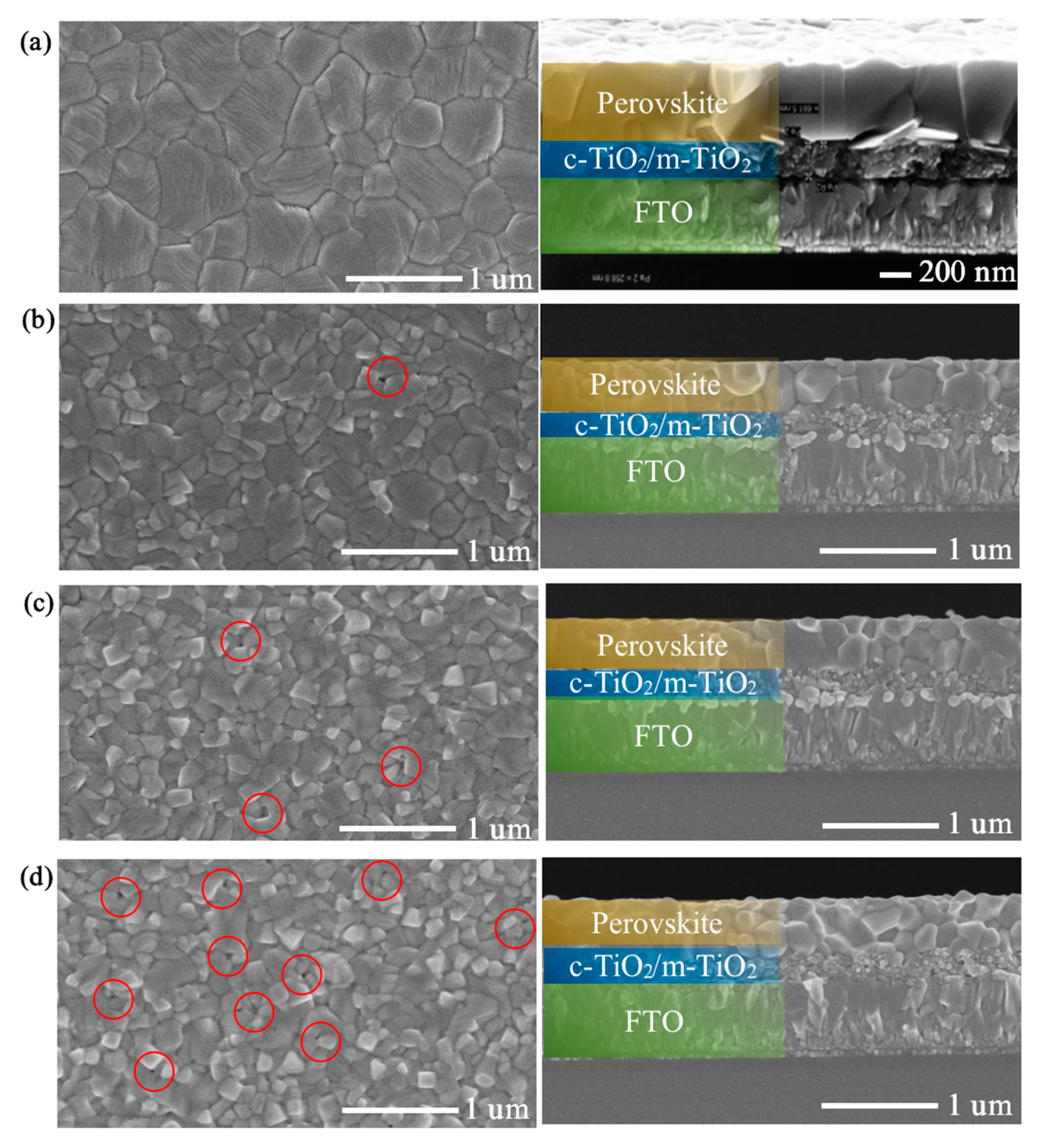
3. Results and Discussion

To explore the quality of Rb-mixed and un-mixed perovskite films firstly, scanning electron microscope (SEM) measurements were measured, as shown in Figure 3. From Figure 3 a, the unmixed MAPbI3 surface is flat and the grain size is larger. From the Rb-mixed SEM top view (Figure 3b–d), it can be seen that smaller grain size start stacked along the vertical direction, and the pinholes began to appear on the surface. The number of pinhole in the perovskite film is more than other films, when the RbI concentrations is further raised to 0.12 mol/L. We considered that the mixing facilitates nucleation of perovskite crystals [34,35]. It can also be seen from the corresponding cross section that with the increase of mixing concentration, the grains gradually become smaller and begin to stack along the vertical direction.
It is shows that the quality of perovskite films are affected with the increase of mixing concentrations. Perovskite grains are stacked vertically, which may lead to lower carrier collection efficiency in PSCs with multi-grain boundaries, since carriers are transported vertically in PSCs. Moreover, with the increase of mixing concentrations, the pinhole of perovskite films gradually increases (as shown in the red circles in Figure 3), which also leads to the decrease of PSCs efficiency.
Supplementary Figure S3 presents the XRD patterns of Rb-mixed perovskite films. It can be seen from Supplementary Figure S3 that the peak positions of all XRD patterns of perovskite do not change significantly, that is, no new peaks appear or disappear after mixing, indicating that the crystal type of perovskite does not change significantly with Rb-mixing of low concentrations.
However, high concentration of Rb-mixing is different from low concentration of Rb-mixing, high concentration (1 mol/L ≤ Rb ≤ 1.5 mol/L) Rb-mixed perovskite is a cubic structure. When the Rb-mixing concentration is increased to 1.8 mol/L, the crystal structure of the perovskite is an orthorhombic structure [23]. The research indicating that low concentration (≤0.12 mol/L) of Rb-mixing does not change the crystal structure of perovskite.
Supplementary Figure S4 shows the EDS diagram of the perovskite films mixed with rubidium ions. It can be seen from the Supplementary Figure S4 that the perovskite films contain rubidium ions. Rb and Si positions have been marked with dotted lines. Rb peak position is 1.6 KeV and Si peak position is 1.7 KeV.
Table 1 shows the majority charge carriers type of Rb-mixed perovskite layers obtained by Hall test. As can be seen from Table 1, the unmixed perovskite layer is N-type, and the perovskite layer is P-type after the mixing of Rb+, which indicates that the two-step rubidium ions mixing has changed the perovskite from N-type to P-type.
Figure 4 shows the UV-vis absorption spectra of perovskite layers with different Rb+ concentrations. As can be seen from the Figure 4, the UV-vis absorption spectra intensity and range of the Rb-mixed perovskite layer have little change. Especially, the absorption band edge of the spectra almost coincide. It indicates that the low concentrations of Rb-mixed has no significant effect on the absorption intensity and band of perovskite optical absorption layer.
The photoluminescence (PL) spectra of the perovskite layer (deposited on TiO2) with different Rb-mixing concentrations are shown in Figure 5. It is clearly observed from Figure 5a that the peak of PL is fairly strong when the concentration of RbI is further increased to 0.12 mol/mL, which could be explained by the existence of pinholes in perovskite films, preventing the photogenerated carriers injecting into the TiO2 layer from the light absorption layer. This is consistent with the results in Figure 3, so we speculate that it may cause JSC to decrease. The PL peaks exhibit a slight blue shift (as shown in Figure 5b), implying a widening of the bandgap and decreasing of the JSC via mixure of Rb [36,37].
Figure 6 shows the J-V curves of PSCs with different Rb+ concentrations. We also have extracted the performance parameters from reverse scanning J-V curves in Figure 6, as shown in Table 2. The short-circuit current density and open circuit voltage of PSCs gradually decrease, which is the main reason why the final efficiency gradually decreases with the increase of Rb-mixed concentrations. It is consistent with the results of film morphology (Figure 3). A number of pinholes in the perovskite film will lead to the decrease of short-circuit current density. However, the efficiency is only slightly decreased, indicating that the P-type perovskite layer and ETL can still form a new P–N hetero-junction after the majority charge carriers type was changed.
The un-mixed and Rb-mixed hetero-junction perovskite device structures are shown in Figure 7. The majority carriers type of perovskite has changed by mixing RbI, indicating that the position of PN junction has changed. In Figure 7a, when the majority carriers type of the un-mixed perovskite layer is N-type, the perovskite layer forms a P–N junction with the Spiro-MeOTAD layer (HTL). In Figure 7b, when the majority carriers type of the Rb-mixed perovskite layer is P-type, the perovskite layer forms a new P–N junction with the TiO2 layer (ETL). We prepared un-mixed and Rb-mixed perovskite solar cells and tested the efficiency of devices (as shown in Table 2). This shows that the newly formed P–N junction can still work.

4. Conclusions

In this paper, the light absorption layer of PSCs was Rb-mixed at low concentrations by the two-step method, and the majority charge carriers type of the perovskite could be changed by mixing Rb+ into the perovskite film. In addition, the Rb-mixed at low concentration has little effect on the crystal structure of perovskite. Moreover, it has little effect on the light absorbing capacity of the perovskite layer. The Rb+ was added to un-mixed N-type perovskite. With the increase of the concentration of Rb+, the quality of perovskite film became worse, the amount of photo-generated carriers injected into the TiO2 layer from the perovskite layer decreases, and the PL peaks exhibit a slight blue shift, resulting in the low device efficiency. However, the efficiency slightly decreased, indicating that the P-type perovskite layer and ETL could still form a new P–N hetero-junction and the PSCs could still work after the majority charge carriers type was changed, which provided a possibility for the homo-junction PSCs.

Supplementary Materials

The following are available online at https://www.mdpi.com/2079-6412/10/7/627/s1, Figure S1: The diagram of sample with the electrode. Figure S2: The schematic diagram of basic test circuit of hall. Figure S3: XRD patterns of perovskite films with different Rb+ concentrations. Figure S4: EDS of perovskite films with different Rb+ concentrations. (a) MAPbI3 (Un-mixed); (b) MAPbI3 (Rb-mixed).

Author Contributions

Conceptualization, X.Z. and T.L.; methodology, T.L.; formal analysis, B.L., T.L., Y.Y., and J.C.; investigation, B.L., T.L., D.C., Y.Y., C.C., X.Y., J.W., Z.Z., and G.L.; data curation, T.L., Y.Y., and J.C.; writing-original draft preparation, B.L. and Y.Y.; writing-review and editing, D.C., X.Y., J.W., Z.Z., G.L., C.C., and X.Z.; visualization, J.C.; supervision, X.Z.; funding acquisition, X.Z. All authors have read and agreed to the published version of the manuscript.

Funding

The authors gratefully acknowledge the Natural Science Foundation of China (No. 61875186), the Natural Science Foundation of Beijing (No. Z160002), the Key Research Projects of BISTU (2019KYNH227) and the Beijing Key Laboratory for Sensors of BISTU (No. 2019CGKF007).

Conflicts of Interest

The authors declare no conflict of interest.

References

  1. Li, X.; Yang, J.; Jiang, Q.; Lai, H.; Li, S.; Tan, Y.; Chen, Y.; Li, S. Perovskite Solar Cells Employing an Eco-friendly and Low-cost Inorganic Hole Transport Layer for Enhanced Photovoltaic Performance and Operational Stability. J. Mater. Chem. A 2019, 7, 7065–7073. [Google Scholar] [CrossRef]
  2. Liu, X.; Cheng, Y.; Liu, C.; Zhang, T.; Zhang, N.; Zhang, S.; Chen, J.; Xu, Q.; Ouyang, J.; Gong, H. 20.7% Highly Reproducible Inverted Planar Perovskite Solar Cells with Enhanced Fill Factor and Eliminated Hysteresis. Energy Environ. Sci. 2019, 12, 1622–1633. [Google Scholar] [CrossRef]
  3. Liang, J.W.; Chen, Z.L.; Yang, G.; Wang, H.B.; Ye, F.H.; Tao, C.; Fang, G.J. Achieving High Open-Circuit Voltage on Planar Perovskite Solar Cells via Chlorine-Doped Tin Oxide Electron Transport Layers. ACS Appl. Mater. Interfaces 2019, 11, 23152–23159. [Google Scholar] [CrossRef] [PubMed]
  4. Dong, Q.; Fang, Y.; Shao, Y.; Mulligan, P.; Qiu, J.; Cao, L.; Huang, J. Electron-hole diffusion lengths > 175 um in solution-grown CH3NH3PbI3 single crystals. Science 2015, 347, 967–970. [Google Scholar] [CrossRef] [Green Version]
  5. Oga, H.; Saeki, A.; Ogomi, Y.; Hayase, S.; Seki, S. Improved Understanding of the Electronic and Energetic Landscapes of Perovskite Solar Cells: High Local Charge Carrier Mobility, Reduced Recombination, and Extremely Shallow Traps. J. Am. Chem. Soc. 2014, 136, 16948. [Google Scholar] [CrossRef]
  6. Yang, G.; Chen, C.; Yao, F.; Chen, Z.; Zhang, Q.; Zheng, X.; Ma, J.; Lei, H.; Qin, P.; Xiong, L.; et al. Effective Carrier-Concentration Tuning of SnO2 Quantum Dot Electron-Selective Layers for High-Performance Planar Perovskite Solar Cells. Adv. Mater. 2018, 30, 1706023.1–1706023.9. [Google Scholar] [CrossRef]
  7. Cao, B.; Yang, L.; Jiang, S.; Lin, H.; Wang, N.; Li, X. Flexible quintuple cation perovskite solar cells with high efficiency. J. Mater. Chem. A 2019, 7, 4960–4970. [Google Scholar] [CrossRef]
  8. Wojciechowski, K.; Stranks, S.D.; Abate, A.; Sadoughi, G.; Sadhanala, A.; Kopidakis, N.; Rumbles, G.; Li, C.Z.; Friend, R.H.; Jen, A.K.; et al. Heterojunction Modification for Highly Efficient Organic-Inorganic Perovskite Solar Cells. ACS Nano 2014, 8, 12701–12709. [Google Scholar] [CrossRef]
  9. Li, C.B.; Wang, A.; Xie, L.S.; Deng, X.Y.; Liao, K.J.; Yang, J.A.; Li, T.S.; Hao, F. Emerging alkali metal ion (Li+, Na+, K+ and Rb+) doped perovskite films for efficient solar cells: Recent advances and prospect. J. Mater. Chem. A 2019, 7, 42. [Google Scholar] [CrossRef]
  10. Bu, T.; Liu, X.; Li, J.; Li, W.; Huang, W.; Ku, Z.; Peng, Y.; Huang, F.; Cheng, Y.B.; Zhong, J. Sub-sized monovalent alkaline cations enhanced electrical stability for over 17% hysteresis-free planar perovskite solar mini-module. Electrochim. Acta 2019, 306, 635–642. [Google Scholar] [CrossRef]
  11. Jacobsson, T.J.; Svanstrm, S.; Andrei, V.; Rivett, J.P.H.; Kornienko, N.; Philippe, B.; Cappel, U.; Rensmo, H.; Deschler, F.; Boschloo, G. Extending the Compositional Space of Mixed Lead Halide Perovskites by Cs, Rb, K, and Na-Doping. J. Phys. Chem. C 2018, 122, 25. [Google Scholar] [CrossRef]
  12. Mahmud, M.A.; Elumalai, N.K.; Upama, M.B.; Wang, D.; Gonɕales, V.R.; Wright, M.; Xu, C.; Haque, F.; Uddin, A. Passivation of interstitial and vacancy mediated trap-states for efficient and stable triple-cation perovskite solar cells. J. Power Sources 2018, 383, 59–71. [Google Scholar] [CrossRef]
  13. Pham, H.T.; Duong, T.; Rickard, W.D.A.; Kremer, F.; Weber, K.J.; Wong-Leung, J. Understanding the Chemical and Structural Properties of Multiple-Cation Mixed Halide Perovskite. J. Phys. Chem. C 2019, 123, 26718–26726. [Google Scholar] [CrossRef]
  14. Zhang, M.; Yun, J.S.; Ma, Q.S.; Zheng, J.H.; Lau, C.F.J.; Deng, X.F.; Kim, J.; Kim, D.; Seidel, J.; Green, M.A.; et al. High-Efficiency Rubidium-Incorporated Perovskite Solar Cells by Gas Quenching. ACS Energy Lett. 2017, 2, 438–444. [Google Scholar] [CrossRef]
  15. Park, I.J.; Seo, S.; Park, M.A.; Lee, S.; Kim, D.H.; Zhu, K.; Shim, H.; Kim, J.Y. Effect of Rubidium Incorporation on the Structural, Electrical, and Photovoltaic Properties of Methylammonium Lead Iodide-Based Perovskite Solar Cells. ACS Appl. Mater. Interfaces 2017, 9, 41898. [Google Scholar] [CrossRef] [PubMed]
  16. Saliba, M.; Matsui, T.; Domanski, K.; Seo, J.Y.; Ummadisingu, A.; Zakeeruddin, S.M.; Correa-Baena, J.P.; Tress, W.R.; Abate, A.; Hagfeldt, A.; et al. Incorporation of rubidium cations into perovskite solar cells improves photovoltaic performance. Science 2016, 354, 206–209. [Google Scholar] [CrossRef]
  17. Duong, T.; Mulmudi, H.K.; Shen, H.; Wu, Y.; Barugkin, C.; Mayon, Y.O.; Nguyen, H.T.; Macdonald, D.H.; Peng, J.; Lockrey, M.N.; et al. Structural engineering using rubidium iodide as a dopant under excess lead iodide conditions for high efficiency and stable perovskites. Nano Energy 2016, 30, 330–340. [Google Scholar] [CrossRef]
  18. Xiao, J.W.; Liang, Y.; Zhang, S.; Zhao, Y.; Li, Y.; Chen, Q. Stabilizing RbPbBr3 Perovskite Nanocrystals through Cs+ Substitution. Chem. A Eur. J. 2018, 25, 2597–2603. [Google Scholar] [CrossRef]
  19. Yao, F.; Gui, P.; Chen, C.; Li, B.; Li, R.; Tao, C.; Lin, Q.; Fang, G. High-Rubidium-Formamidinium-Ratio Perovskites for High-Performance Photodetection with Enhanced Stability. ACS Appl. Mater. Interfaces 2019, 11, 39875–39881. [Google Scholar] [CrossRef]
  20. Arjaan, K.; Loreta, A.M.; René, M.W. Perovskite Thin Film Materials Stabilized and Enhanced by Zinc (II) Doping. Appl. Sci. 2019, 9, 1678. [Google Scholar]
  21. Wang, Q.; Shao, Y.; Xie, H.; Lyu, L.; Liu, X.; Gao, Y.; Huang, J. Qualifying composition dependent p and n self-doping in CH3NH3PbI3. Appl. Phys. Lett. 2014, 105, 163508. [Google Scholar] [CrossRef] [Green Version]
  22. Cui, P.; Wei, D.; Ji, J.; Huang, H.; Jia, E.; Dou, S.; Wang, T.; Wang, W.; Li, M. Planar p–n homojunction perovskite solar cells with efficiency exceeding 21.3%. Nat. Energy 2019, 4, 150–159. [Google Scholar] [CrossRef]
  23. Bai, X.; Zou, X.P.; Zhu, J.L.; Pei, Y.X.; Yang, Y.; Jin, W.B.; Chen, D. Effect of Rb-doping on modulating grain shape and semiconductor properties of MAPbI3 perovskite layer. Mater. Lett. 2018, 21, 328–330. [Google Scholar] [CrossRef]
  24. Saleem, A.; Imran, M.; Arshad, M.; Kamboh, A.H.; Khan, N.A.; Haider, M.I. Investigation of Rbx(MA)1−xPbI3(x  =  0, 0.1, 0.3, 0.5, 0.75, 1) perovskites as a potential source of P- and N-type materials for PN-junction solar cell. Appl. Phys. 2019, 125, 229. [Google Scholar] [CrossRef]
  25. Yao, Y.J.; Zou, X.P.; Cheng, J.; Ling, T.; Chang, C.C.; Chen, D. Impact of K+ Doping on Modulating Majority Charge Carrier Type and Quality of Perovskite Thin Films by Two-step Solution Method for Solar Cells. Coatings 2019, 9, 647. [Google Scholar] [CrossRef] [Green Version]
  26. Liu, X.X.; Li, B.C.; Zhang, N.D.; Yu, Z.M.; Sun, K.; Tang, B.S.; Shi, D.W.; Yao, H.Y.; Ouyang, J.Y.; Gong, H. Multifunctional RbCl dopants for efficient inverted planar perovskite solar cell with ultra-high fill factor, negligible hysteresis and improved stability. Nano Energy 2018, 53, 567–578. [Google Scholar] [CrossRef]
  27. Burschka, J.; Pellet, N.; Moon, S.J.; Humphry-Baker, R.; Gao, P.; Nazeeruddin, M.K.; Grätzel, M. Sequential deposition as a route to high-performance perovskite-sensitized solar cells. Nature 2013, 499, 316–319. [Google Scholar] [CrossRef]
  28. Im, J.H.; Kim, H.S.; Park, N.G. Morphology-photovoltaic property correlation in perovskite solar cells: One-step versus two-step deposition of CH3NH3PbI3. APL Mater. 2014, 2, 591–713. [Google Scholar] [CrossRef] [Green Version]
  29. Wang, M.H.; Feng, Y.L.; Bian, J.M.; Liu, H.Z.; Shi, Y.T. A comparative study of one-step and two-step approaches for MAPbI3 perovskite layer and its influence on the performance of mesoscopic perovskite solar cell. Chem. Phys. Lett. 2018, 692, 44–49. [Google Scholar] [CrossRef]
  30. Chang, C.C.; Zou, X.P.; Cheng, J.; Ling, T.; Yao, Y.Y.; Chen, D. Influence of Solution Deposition Process on Modulating Majority Charge Carrier Type and Quality of Perovskite Thin Films for Solar Cells. Materials 2019, 12, 2494. [Google Scholar] [CrossRef] [Green Version]
  31. Zhang, N.N.; Guo, Y.J.; Yin, X.; He, M.; Zou, X.P. Spongy carbon film deposited on a separated substrate as counter electrode for perovskite-based solar cell. Mater. Lett. 2016, 182, 248–252. [Google Scholar] [CrossRef]
  32. Yao, Y.J.; Zou, X.P.; Cheng, J.; Chen, D.; Chang, C.C.; Ling, T.; Ren, H.Y. Impact of Delay Time before Annealing MAI-PbI2-DMSO Intermediate Phase on Perovskite Film Quality and Photo-Physical Properties. Crystals 2019, 9, 151. [Google Scholar] [CrossRef] [Green Version]
  33. Ling, T.; Zou, X.P.; Cheng, J.; Yang, Y.; Ren, H.Y.; Chen, D. Modulating Surface Morphology Related to Crystallization Speed of Perovskite Grain and Semiconductor Properties of Optical Absorber Layer under Controlled Doping of Potassium Ions for Solar Cells. Materials 2018, 11, 1605. [Google Scholar] [CrossRef] [PubMed] [Green Version]
  34. Zhou, Y.; Game, O.S.; Pang, S.; Padture, N.P. Microstructures of Organometal Trihalide Perovskites for Solar Cells: Their Evolution from Solutions and Characterization. J. Phys. Chem. Lett. 2015, 6, 4827–4839. [Google Scholar] [CrossRef]
  35. Zhou, Z.M.; Qiang, Z.Y.; Sakamaki, T.; Takei, I.; Shang, R.; Nakamura, E. Organic/Inorganic Hybrid p-Type Semiconductor Doping Affords Hole Transporting Layer Free Thin-Film Perovskite Solar Cells with High Stability. ACS Appl. Mater. Interfaces 2019, 11, 22603–22611. [Google Scholar] [CrossRef] [PubMed]
  36. Park, Y.H.; Jeong, I.; Bae, S.; Son, H.J.; Lee, P.; Lee, J.; Lee, C.H.; Ko, M.J. Inorganic Rubidium Cation as an Enhancer for Photovoltaic Performance and Moisture Stability of HC(NH2)2PbI3 Perovskite Solar Cells. Adv. Funct. Mater. 2017, 27, 1605988.1–1605988.9. [Google Scholar] [CrossRef]
  37. Kim, H.; Byun, H.R.; Jeong, M.S. Synthesis and Characterization of Multiple-Cation Rb(MAFA)PbI3 Perovskite Single Crystals. Sci. Rep. 2019, 9, 2022. [Google Scholar] [CrossRef]
Figure 1. Schematic preparation procedure of the perovskite films by using two-step method.
Coatings 10 00627 g001
Figure 2. Schematic illustration with the structure of PSC.
Coatings 10 00627 g002
Figure 3. SEM images of surface and cross section of perovskite films with different Rb+ concentrations. (a) MAPbI3; (b) MAPbI3 + 0.04 RbI; (c) MAPbI3 + 0.08 RbI; (d) MAPbI3 + 0.12 RbI. Red circles: The pinholes in the perovskite films are marked by the red circles.
Coatings 10 00627 g003
Figure 4. UV-vis absorption spectra of perovskite layer with different Rb+ concentrations.
Coatings 10 00627 g004
Figure 5. PL spectra of perovskite flims deposited on TiO2 with different Rb-mixing concentration. (a) The PL spectra; (b) The normalized PL spectra.
Coatings 10 00627 g005
Figure 6. Reverse scanning current-Voltage (J-V) curves of PSCs of FTO/c-TiO2/m-TiO2/perovskite/Spiro-OMeTAD/Spongy Carbon/FTO.
Coatings 10 00627 g006
Figure 7. The un-mixed and Rb-mixed hetero-junction perovskite device structures. (a) The un-mixed perovskite device structure; (b) the Rb-mixed perovskite device structure. E: built-in electric field.
Coatings 10 00627 g007
Table 1. Hall parameters of perovskite layer with different Rb+ concentrations.
SamplesHall Parameters
Mob a (cm2/Vs)N b (/cm3)Types c
MAPbI3169−3.9 × 10¹²n
MAPbI3 + 0.04 RbI76.2+6.9 × 10¹²p
MAPbI3 + 0.08 RbI58.5+5.9 × 10¹³p
MAPbI3 + 0.12 RbI79.2+2.9 × 10¹³p
Note: a. Mob: Mobility; b. N: Carrier concentration; c. Types: Majority charge carriers type.
Table 2. Parameters extracted from reverse scanning Current-Voltage (J-V) curves of perovskite solar cells with different Rb+ concentrations.
SamplesVOCa (V)JSCb (mA/cm2)FF c (%)PCE d (%)
MAPbI30.9819.9956.6311.09
MAPbI3 + 0.04 RbI0.9619.7755.0710.41
MAPbI3 + 0.08 RbI0.9419.5849.209.04
MAPbI3 + 0.12 RbI0.9117.4756.248.90
Notes: a. VOC: open-circuit voltage; b. JSC: short-circuit current; c. FF: fill factor; d. PCE: power conversion efficiency.

