Article

Low-Temperature Fabrication of High-Performance and Stable GZO/Ag/GZO Multilayer Structures for Transparent Electrode Applications

by
Akmedov K. Akhmedov
1,
Aslan Kh. Abduev
1,
Vladimir M. Kanevsky
2,
Arsen E. Muslimov
2 and
Abil Sh. Asvarov
1,2,*
1
Institute of Physics, Dagestan Federal Research Center, Russian Academy of Sciences, 367015 Makhachkala, Russia
2
Shubnikov Institute of Crystallography, Federal Scientific Research Center Crystallography and Photonics, Russian Academy of Sciences, 119333 Moscow, Russia
*
Author to whom correspondence should be addressed.
Coatings 2020, 10(3), 269; https://doi.org/10.3390/coatings10030269
Submission received: 13 February 2020 / Revised: 10 March 2020 / Accepted: 12 March 2020 / Published: 13 March 2020
(This article belongs to the Special Issue Optical Thin Films and Structures: Design and Advanced Applications)

Abstract

:
Presently, research and development of indium-free stable highly transparent conductive (TC) materials is of paramount importance for the blooming world of information display systems and solar energy conversion. Development of devices based on flexible organic substrates further narrows the choice of possible TC materials due to the need for lower deposition and process temperatures. In our work, the structural, electrical, and optical performances of Ga-doped ZnO/Ag/Ga-doped ZnO (GZO/Ag/GZO) multilayered structures deposited on glass substrates by direct current (DC) magnetron sputtering in a pure Ar medium without any purposeful substrate heating have been investigated. The highest figure of merit achieved was 5.15 × 10⁻² Ω−1 for the symmetric GZO/Ag/GZO multilayer, featuring GZO and Ag thicknesses of 40 and 10 nm, respectively, while the average optical transmittance was over 81% in the visible range of wavelengths and the resistivity was 2.2 × 10⁻⁵ Ω·cm. Additionally, the good durability of the performances of the multilayer structures was demonstrated by their testing in the context of long-term storage (over 500 days) in standard environmental conditions.

1. Introduction

Transparent electrodes (i.e., thin films based on transparent conductive (TC) materials) are some of the most important parts of many optoelectronic devices, such as touch panels, organic light-emitting diodes (OLEDs), optical sensors, and solar cells [1,2,3,4,5].
Nowadays, transparent electrodes based on Sn-doped In2O3 (ITO) present outstanding optoelectronic performance and have been widely used in various commercial domains [1,6]. However, the wide use of ITO transparent electrodes in optoelectronic devices is gradually pushing up the cost of ITO electrodes because indium is not abundant on Earth. Moreover, with the rapid development of new types of display systems, sensors, and solar energy, new requirements for transparent electrodes are emerging from device developers, in addition to their transparency and conductivity. It is getting harder for the traditional ITO electrodes to meet the new requirements. Therefore, alternative materials should be developed.
A variety of ITO replacements have been investigated, including doped wide-bandgap oxides with high transmittance, such as SnO2 [7], ZnO [8,9], and TiO2 [10]. However, these oxides were found to have lesser performance than ITO, combining both electrical and optical properties. As alternatives to ITO, poly(3,4-ethylenedioxythiophene):poly(4-styrenesulfonate) (PEDOT–PSS) [11], graphene [12], carbon nanotubes [13], and metal nanowires and meshes [14,15] have been proposed. However, each alternative solution is affected by one or more drawbacks that prevent their widespread use [16,17].
In order to keep a low resistance and conversely maintain high optical transmittance, oxide–metal–oxide multilayered structures have recently received renewed interest as a highly promising route towards the production of flexible large area OLEDs and solar cells [3,18,19,20]. In this case, Ag is the optimal metal because of its low resistivity (approximately 1.6 × 10⁻⁶ Ω∙cm) and relatively low cost [21], whereas Ga-doped ZnO (GZO) is the optimal oxide due to its abundance, low cost, superior optical features, and rather high stability [22,23].
Various deposition techniques have been used to produce oxide–metal–oxide structures, including thermal evaporation [24], electron beam evaporation [25], spray pyrolysis [26], sol–gel methods [27], ion beam sputtering [28], and magnetron sputtering [18,19,20,28]. Low-cost wet chemical methods are usually the starting point and benchmark for most academic and industrial processes that require a thin and uniform coating, but the transparent electrodes obtained by these techniques have resulted in inferior electrical features compared with those deposited by ion plasma methods [25,29,30]. In this sense, it appears that DC magnetron sputtering is the most promising technique in terms of the industrial deposition of uniform films at a proper deposition rate [18]. From the point of view of the deposition of transparent electrodes on flexible substrates covering a large area, it is also very important to achieve TC films with good performance stability by using low-temperature processes [28,31].
In this article, symmetric GZO/Ag/GZO (GAG) multilayered structures were sequentially formed on glass substrates by room temperature DC magnetron sputtering under a pure Ar atmosphere. The uniqueness and novelty of this work resides in having found the process conditions that provide the optimal trade-off between low resistivity and high optical transmittance and are applicable for TC thin film formation on polymer substrates. The thicknesses of GZO and Ag layers were parametrized to get the optimal optical and electrical properties of the superstructures. The deposited multilayers were characterized and tested for their structural, electrical, optical, and adhesive properties.

2. Materials and Methods

GAG multilayered structures were deposited on glass and surface-oxidized Si pieces by DC magnetron sputtering method using a Magnetron setup (Russia) equipped with two sputtering units. The base pressure of the chamber was maintained at 2 × 10⁻⁴ Pa.
The bottom and top oxides layers were deposited using Ga (3 at.%)-doped ZnO target under the following deposition conditions: Ar working pressure of 0.5 Pa, discharge current of 270 mA, discharge voltage of 720 V. The Ag thin interlayer was deposited using an Ag (99.99%) pure target under the following conditions: Ar working pressure of 0.5 Pa, discharge current of 150 mA, discharge voltage of 750 V. Before the formation of each layer of the GAG trilayered structure, a presputtering cycle of both GZO and Ag targets on a closed shutter was performed for 10 and 3 min, respectively. The distance between targets and substrates was 150 mm. The substrates revolved at a rate of 30 r/min. The substrate was not specially heated during the growth of multilayers, but there was a slight heating to about 50 °C due to ion bombardment. The growth rates for the oxide and metal components of the three-layer structure under such conditions were 1.33 and 3.00 nm/min, respectively. The thickness of oxide and metal components of the GAG multilayer was controlled by varying the deposition time, which was the same for bottom and top GZO films in order to create a symmetric trilayer structure. Layer thickness variations were also confirmed by cross-sectional scanning electron microscopy (SEM) and were consistent with the estimated depositing times (Figure S1 of Supplementary Materials (SM)).
Table 1 shows thickness data of seven multilayered samples with various geometries. For the first five samples (from GAG-0 to GAG-4), the thicknesses of the silver interlayer were varied between 0 and 12 nm, while keeping fixed thicknesses for oxide top and bottom GZO layers (40 nm). For the samples GAG-5 and GAG-6, the thickness of oxide films was varied, keeping the thickness of the Ag interlayers fixed (10 nm). For comparison, a two-layered GA with a 80-nm thick bottom oxide and thin upper metal layer (10 nm) was deposited additionally.
The surface morphologies of the deposited samples were investigated by using a Leo-1450 scanning electron microscope (SEM) (Carl Zeiss) and a Ntegra Prima atomic force microscope (NT-MDT SI). X–ray diffraction (XRD) patterns were collected on a X’PERT PRO MPD diffractometer (PANalytical) with CuKα radiation (λ = 1.5418 Å). The electrical properties were measured by using the four-probe technique (IUS-3, Russia). Optical transmittance spectra were obtained by a UV-3600 optical spectrophotometer (Shimadzu) in the wavelength range of 340–1240 nm. All of the measurements were carried out at room temperature.

3. Results and Discussion

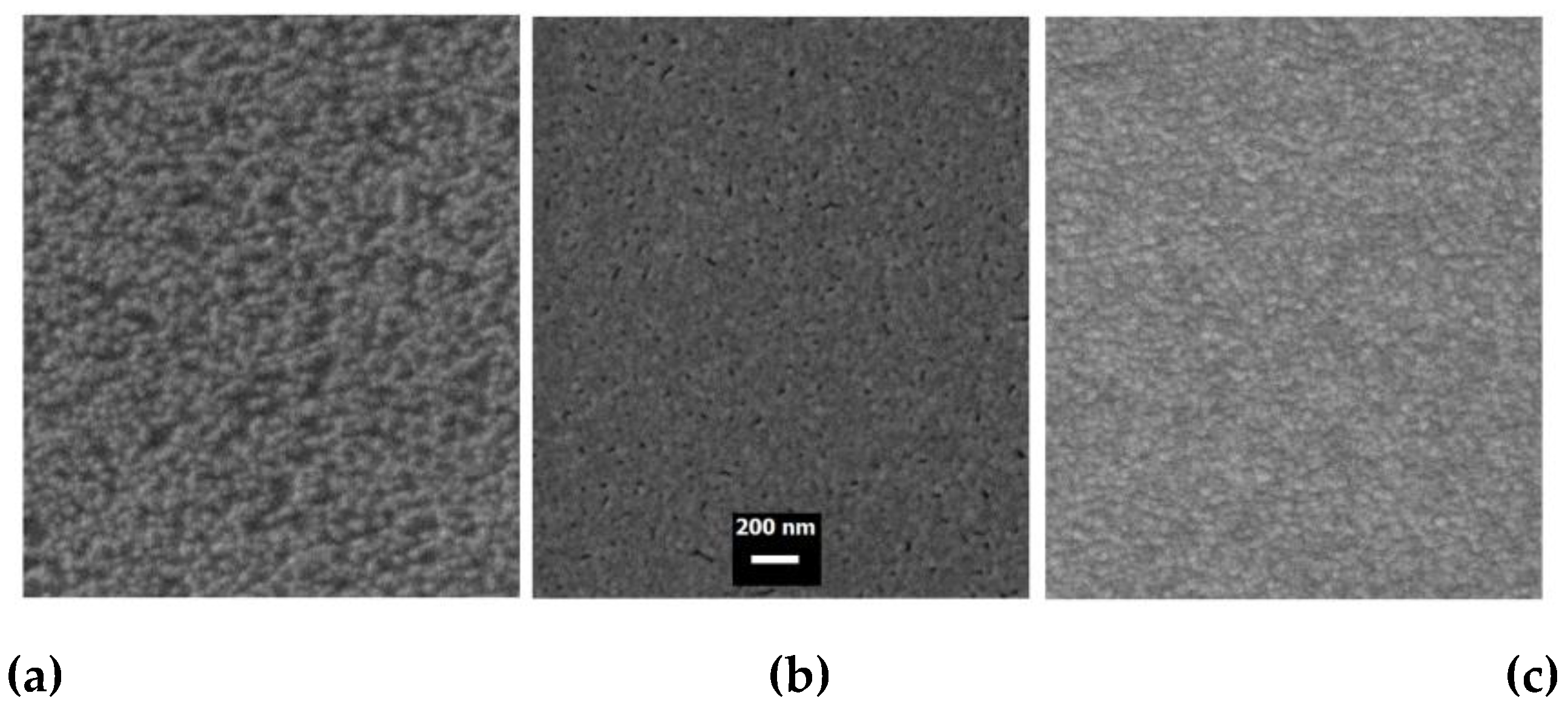
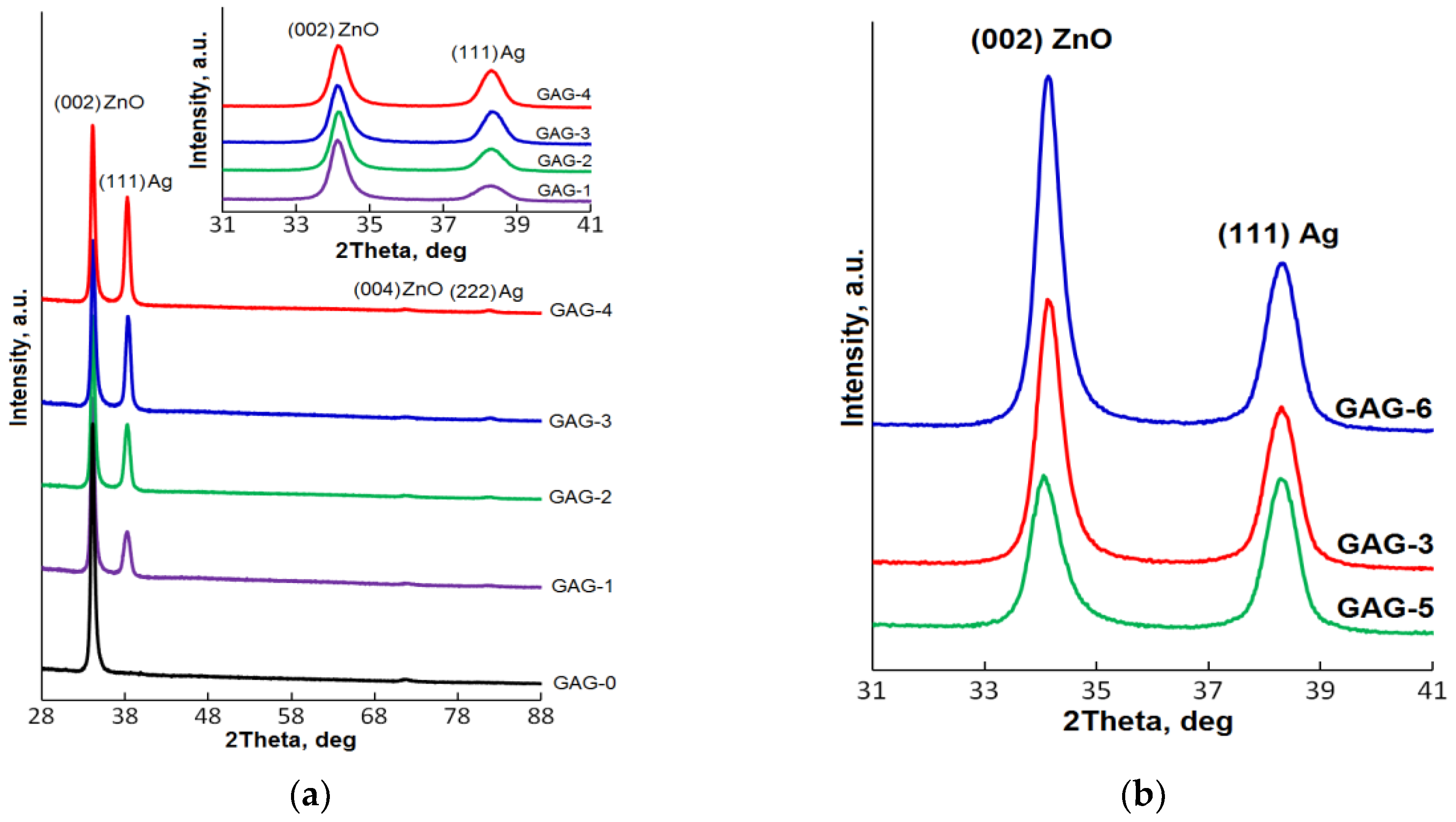
3.1. Surface Morphology and Structural Studies

The surface morphology of the GAG samples was investigated by SEM. Figure 1 shows the typical SEM images of top view surfaces observed in this work. A single layer GAG-0 sample with a total thickness of oxide of 80 nm and a zero thickness Ag interlayer (Figure 1a) consists of well-defined continuous particles of nearly equal lateral size (~ 40 nm) uniformly covering the smooth substrate. After deposition of 10-nm thick Ag layer on the GZO surface, a well-marked change in morphology appears (Figure 1b). Forming a sufficiently continuous layer of silver makes the surface of the structure even smoother, although some nanovoids on the surface of the GA bilayered structure are still present due to the surface performance of the bottom GZO layer. The observed smoothing of the surface indicates that under the above growth conditions, the process of Ag growth should be described in the following scenario:
  • At the initial stage of growth, a large number of silver nuclei are formed on the surface of the GZO layer due to limited migration of adatoms;
  • The high density of the nuclei contributes to their earlier coalescence into a continuous metal film, covering the GZO surface [32].
In earlier reports [33,34], it was found that the spreading of Ag on the surface of ZnO was better than on SnO2 and In2O3 due to an ameliorated affinity between Ag and ZnO. Nevertheless, it was confirmed that the surface of ZnO was rougher than that of the latter.
As is shown in Figure 1c, the surface morphology of GAG-3 trilayered structure became less smooth but quite compact. The difference between the surfaces of GAG-1 and GAG-3 samples is due to both differences in the nucleation conditions of the top and bottom oxide layers, and the fact that the grain size usually increases with the thickness of the ZnO thin film [35,36].
It should be noted that the SEM studies of other samples did not reveal any noticeable differences in the surface morphology of the samples considering the thickness of the Ag interlayer at a fixed thickness of the GZO, as well as when changing the thickness of the GZO layers in the range of 30–50 nm. Thus, we can reach a conclusion that in our SEM experiment, the top GZO, which was sputtered at room temperature, showed surface features typical of nanocrystalline Ga-doped ZnO thin films, regardless of the Ag interlayer thickness and its morphology. At the same time, additional atomic-force microscopy (AFM) studies (Figure S2 in SM) showed that the surface roughness increases noticeably by introducing an Ag interlayer into GZO. The root mean square (RMS) roughness values of GZO-0 and GZO-1 samples are 0.897 and 1.226 nm, respectively, calculated from the AFM data. A slight decrease in roughness is observed with further increases of both Ag and GZO thicknesses in the trilayer structures.
Figure 2a shows the XRD plots of the GAG multilayered structures with Ag interlayers of different thicknesses. Only four broad peaks were present in the XRD spectra, two of which belong to the (002) ZnO and (004) ZnO reflections, and the other two to the (111) Ag and (222) Ag reflections. The presence of two (002) ZnO and (004) ZnO peaks corresponding to the nanocrystalline hexagonal ZnO wurtzite phase indicates that the GZO has a preferential orientation featuring the c-axis perpendicular to the substrate surface, regardless of the Ag interlayer thickness. The insertion of the Ag interlayer in the middle of the GAG structure does not affect the strongly preferred orientation of GZO toward (001). Additionally, for the GAG structures, the Ag interlayer has highly preferred orientation toward (111). It is often reported that the crystallized ZnO lattice promotes the silver growth along the (111) direction. This might be due to the fact that the (111) plane of a cubic structure has a similar symmetry to that of the (001) plane of ZnO [34]. The inset of Figure 2a shows the XRD spectral region in which the most intense (002) ZnO and (111) Ag peaks are located. The main features of both peaks are given in Table 2.
It can be seen that when the Ag interlayer is introduced into the GAG structure, thereby breaking the GZO layer into two equal parts by thickness, a decrease in intensity and some broadening of the (002) ZnO peak takes place. A further increase of the thickness of the Ag interlayer until 12 nm does not affect the crystallinity of the GZO phase, which is correlated with the SEM data results.
At the same time, the intensity of the (111) Ag peak increases and the integral breadth β decreases with a thickening of the Ag interlayer. The peak shifts from 38.21 to 38.25°, with an increase in the Ag thickness from 6 to 8 nm, after which its position no longer changes.
Estimation of the averaged crystallite size (CS) from (002) ZnO and (111) Ag peak characteristics using the Scherrer equation (CS = 0.9λ/(βcosθ), where λ is the wavelength of CuKα x-rays, β is the peak integral breadth with no instrumental contribution, and θ is the peak Bragg angle) showed that the crystallite size of GZO decreases from 16 to 14 nm when the Ar interlayer is introduced, and the Ag crystallite size increases continuously with the increase of the Ag thickness from 7 to 10 nm.
The change in the ratio of the intensities I of the (111) Ag and (002) ZnO peaks (IAg/IZnO) is in agreement with the deposition regimes for these GAG structures.
Despite the low substrate temperature during the GZO and Ag sputtering process, the GAG multilayer structures consist of both nanocrystalline GZO and Ag layers (Figure S3 of SM). In addition, we can reach the conclusion that the crystallinity of the top GZO layer is independent of the Ag interlayer.
GZO thickness variation in the range of 30–50 nm at a fixed thickness of the Ag interlayer of 10 nm does not affect the preferential orientation of both GZO and Ag layers. Figure 2b shows the XRD plots of the GAG structures as a function of the top and bottom GZO thickness in the 2θ range of 31–41°. XRD data for (002) ZnO and (111) Ag peaks of GAG-5 and GAG-6 are shown in Table 2 (in order to compare these with GAG-3).
Comparing these samples, the (002) ZnO peak shifts from 34.01 to 34.10° with an increase in the GZO thickness from 30 to 40 nm. A further increase of the GZO thickness does not change the peak position at 34.10. It can also be observed that as the thickness of GZO film increases, the intensity I is enhanced and the integral breadth β decreases for the (002) ZnO diffraction peak, indicating that the increased thickness of top and bottom layers improves the crystallinity of the GZO phase.
As for the (111) Ag peak, its features for this sample group were practically independent of the thickness of the oxide layers, which implies the invariability of the crystallinity of the Ag interlayer with the increase of the GZO thickness. By increasing the GZO thickness, the averaged crystallite size for GZO increases continuously from 12 to 15 nm, while the Ag crystallite size remains unchanged and remains in good agreement with the thickness of the Ag interlayer.
Thus, we can conclude that the crystallinity of the Ag interlayer is insensitive to changes in the thickness of the bottom GZO layer for the low substrate temperature sputtering process. In this case, the presence of this GZO layer itself is important as a seed layer for Ag. Changes in the nature of coalescence of Ag nuclei were observed in the presence of seed layers with a thickness of only a few nanometers [37,38].

3.2. Optical and Electrical Studies

The GAG-0 sample without any silver interlayer showed a high sheet resistance RS of 2500 Ω/sq and electrical resistivity ρ in the order of 10−2 Ω·cm due to the low preparation temperature. The optical transmittance of GAG-0 is 88% in the visible range of wavelengths (400–700 nm), as shown in Figure 3a, which is consistent with early studies [23,26]. After covering this GZO film with the 10-nm thick Ag layer (GA sample), the resistivity decreases to 2.3 × 10⁻⁵ Ω·cm. It is obvious that the conductivity of such a two-layer structure is mainly governed by the continuity and homogeneity of the Ag thin layer [39]. However, as can be seen from Figure 3a, the existence of the Ag layer on top of the 80-nm thick GZO layer substantially reduces the optical transmittance in the visible and near infrared (NIR) regions (the average visible transmittance Tav is 41.5%) [28].
In Figure 3a, the optical transmittance spectra are presented of the GAG trilayered structures, consisting of two identical 40-nm GZO layers and Ag interlayers with different thicknesses. As shown in the figure, the top GZO layer antireflects the Ag layer in GAG structures to output higher transmittances than the GA bilayer structure by itself [40]. Moreover, the optical transmittances of the GAG multilayers were found to depend critically on the Ag interlayer thickness.
The average optical transmittance in the visible wavelength Tav region of the GAG-1 sample is relatively low (75%) due to light scattering on various defects (pores inherent in ultrathin Ag films and resulting imperfections of the GZO–Ag interfaces). By increasing the Ag thickness to 10 nm, the average optical visible transmittance increases and there is a shift of the transmission peak due to the effects of surface plasmon resonance of the Ag interlayer with minimum voids [41]. In particular, GAG-3 shows high optical transmittance in the visible region, with maximum transmittances of approximately 89% at λ = 529 nm. Next to a wavelength of 550 nm, this sample has the highest optical transmittance, which is even higher than that of GAG-0, which has no silver interlayer.
Further increasing the Ag thickness above 10 nm results in a decrease of the transmittance because of increased light reflection from the continuous Ag interlayer. Additionally, all samples show an abrupt decrease in optical transmittance in the near infra-red region, which is correlated with the thickness of the metal interlayer and attributed to the reflection of long-wavelength light by the layered metal [33]. Thus, the best optical properties of the GAG structures are obtained when the Ag interlayer thickness is 10 nm. The obtained optimal thickness value of the Ag interlayer is similar to the one reported by other groups for ZnO/Ag/Zno multilayers deposited at low substrate temperatures [19,28,42,43,44].
Figure 3b depicts the transmittance spectra for the GAG structures with the optimum Ag interlayer thickness and different GZO thicknesses. With the increase of GZO thickness, the transmittance first shows an increase and then decreases. Simultaneously, the peak transmittance shifts towards the long wavelength regions. For clarity, the results of our optical measurements are summarized in the corresponding columns of Table 3. Based on these results, the GAG-3 sample with 40-nm thick GZO top and bottom layers and a 10-nm thick Ag interlayer was considered as the optimum choice in terms of optical properties.
The results of our study on the dependence of electrical properties of the multilayer samples as sheet resistance resistivity (RS) and resistivity (ρ) on the thicknesses of the GZO and Ag layers are also presented in Table 3.
According to the presented results, the resistivity ρ can be decreased drastically by three orders of magnitude by inserting a thin Ag interlayer. From the fact that even at the Ag thickness of 6 nm, the specific resistance of the GAG-1 is significantly reduced, it can be assumed that in this case the Ag interlayer is already a continuous network of partially coalesced islands. The material of the top GZO layer partially fills the voids of Ag, therefore additionally shunting the gaps in the metal network. A further increase in the thickness of the Ag interlayer results in both an improvement in the crystalline perfection of the metal phase and a decrease in the size and number of voids in it. Thus, a monotonic decrease in resistance with increasing thickness of the Ag interlayer can be explained by an obvious increase in the total number of charge carriers (the effective carrier concentration) in GAG and also very likely by an increase of carrier mobility.
From the comparison of the electrical properties of the GAG-3, GAG-5, and GAG-6 samples (GZO thickness variation at a fixed Ag thickness of 10 nm), we can verify that the oxide layers in the oxide–Ag–oxide multilayer play only a minor role in the electrical properties of the conductive multilayer structures [45]. While the surface resistance decreases from 2.8 to 2.2 Ω/sq with increasing GZO thickness, there is an increase in resistivity from 2 × 10⁻⁵ to 2.45 × 10⁻⁵ Ω∙cm.
Assuming that the total number of carriers in the metal layer (NAg) is much greater than the number of carriers in the oxide layer (NGZO), the effective concentration of carriers (n) of the symmetric GAG structure is related to the thickness of the GZO layers by the following expression [46]:
n ~ NAg / (2 × dGZO + dAg)
where dAg and dGZO are the thickness of the metal interlayer and top (bottom) oxide layer, respectively. From this relation, it can be clearly seen that the carrier concentration should be decreased as the GZO layer thickness increases. This is consistent with the above experiment results.
To evaluate the performance of transparent conductive films for various applications, the optical transmission and the electrical conduction of the films should not be considered separately. Simultaneous optimization of low resistivity and transparencies is needed. Usually, the objective evaluation can be carried out using Haacke’s figure of merit (FOM) [47], defined as:
FOM = T10 / RS
where T is the transmittance at λ = 550 nm or the average visible transmittance. In the last column of Table 3, there are FOM values, which are calculated by using the value of the average visible transmittance Tav for the all deposited samples. From samples of Ag of varying thickness, the maximum FOM of 5.15 × 10⁻² Ω−1 corresponds to GAG-3, with Ag thickness measuring 10 nm and sheet resistance of 2.45 Ω/sq. This is despite the fact that GAG-4, with Ag thickness of 12 nm, showed a record low resistance (2.0 Ω/sq.). As can be seen, GAG-3 also demonstrates the maximum FOM value when comparing samples with the same Ag layer thickness. Additionally, for this sample the FOM’ was also calculated by using the value T550nm of the transmittance at λ = 550 nm (this parameter is usually used to characterize transparent electrodes for LED and information display applications). The value of FOM’ is equal 1.27 × 10⁻¹ Ω−1 due to the highest transmittance at 550 nm. Both values of the figure of merit of GAG-3 are superior to many of those reported in the literature [19,44,45,46]. This may be due to the better spreadability of the Ag layer on the GZO layer during DC magnetron deposition at low temperature, where the bottom GZO layer enhances the silver thin film crystallite size [34,48]. This prompts the formation of a uniform and continuous Ag layer at a much thinner thickness, thereby significantly improving its transparency and conductivity characteristics.

3.3. Adherence and Durability Tests

In order to test the adherence of the GAG structures, the scotch tape test was carried out for all the deposited samples. All the GAGs were found to withstand the scotch tape test as soon as prepared and after 500 days of exicator-free storage in paper envelopes. Long-term indoor storage at an average annual humidity and temperature of 65% and 24 °C, respectively, did not lead to any deterioration of the performance of our GAG samples, whereas in the bilayer GA sample, a lot of white dots and spots with fractal-like structures appeared after 45 days [49]. After this, its optical and electrical performance became unacceptable. This result reveals an additional important role of the upper GZO layer as a protective layer, blocking the damaging effects of moisture on the thin Ag layer. Thus, the trilayer GAG structures have good long-term durability and their adherence to the substrate is good.

4. Conclusions

The GZO/Ag/GZO multilayer structures were deposited sequentially by using DC mode only in the magnetron sputtering for both oxide and metal components of the multilayer structure in pure Ar medium and without any purposeful substrate heating. We investigated the structural, electrical, and optical properties of multilayer structures deposited in various combinations of thicknesses of the Ag interlayer and GZO layers. Comparison between XRD, SEM, and electro-optical performance data with each other, as well as with the data from other authors, allows us to draw the following conclusions:
  • The bottom nanocrystalline GZO layer contributes to the earlier formation of the continuous Ag layer with highly preferred orientation toward(111);
  • The earlier coalescence of Ag nanocrystallites makes it possible to achieve high conductivity for the ultra-thin metal interlayer, characterized by low scattering and lowered plasmonic and intrinsic absorption;
  • The top GZO layer, in addition to the antireflection effect, also acts as a protective layer, effectively blocking the interaction of the nano-Ag phase in the presence of external humidity.
The highest FOM value was 5.15 × 10⁻² Ω−1 for the symmetric GZO/Ag/GZO multilayer with GZO and Ag thicknesses of 40 and 10 nm, respectively, and was achieved when optimizing the geometry of the multilayered structure. This multilayer structure has an average visible transmittance of above 81% and resistivity of 2.2 × 10⁻⁵ Ω∙cm, values that were unchanged after 500 days storage in a normal environment. In conclusion, using only DC mode in magnetron sputtering and the absence of substrate heating during sample preparation in the context of this work makes our results very promising in terms of further industrial compatibility.

Supplementary Materials

The following are available online at https://www.mdpi.com/2079-6412/10/3/269/s1, Figure S1: Cross-sectional SEM images of the GAG-3 (a) and GAG-4 (b) trilayer structures, Figure S2: AFM images (2×2 μm2) prepared in semi-contact mode for GAG-0 (a), GAG-1 (b), GAG-3 (c), GAG-4 (d), GAG-5 (e), and GAG-6 (f), Figure S3: GAG-3 XRD plot in comparison with XRD spectra of pure bulk Ag and pure bulk ZnO materials.

Author Contributions

A.K.A. and A.Sh.A. carried out most of the deposition and testing experiments. A.K.A., A.E.M. and A.Sh.A. performed the investigations of samples properties. A.Sh.A., A.Kh.A. and V.M.K. analyzed the data. Writing—original draft preparation, A.K.A. and A.Sh.A. Writing—review and editing, A.Sh.A. In this study, A.Kh.A. and V.M.K. provided the financial and technical support for designing and conducting the research, as well as supervised the whole research process. All authors have read and agreed to the published version of the manuscript.

Funding

This research was performed in the frame of state assignments of Ministry of Science and Higher Education of the Russian Federation for Dagestan Federal Research Center of Russian Academy of Sciences (Dagestan FRC of RAS) and Federal Scientific Research Center “Crystallography and Photonics” of Russian Academy of Sciences (FSRC "Crystallography and Photonics" RAS) and partially funded by Russian Foundation for Basic Research (research project no. 18-29-12099 and no. 19-07-00537). Access to the equipment of the Shared Research Center of FSRC “Crystallography and Photonics” RAS was supported by the Ministry of Science and Higher Education of the Russian Federation (project RFMEFI62119X0035).

Acknowledgments

The authors are grateful for additional technical support from the Shared Research Centers of Dagestan FRC of RAS. The authors acknowledge Alessandro Chiolerio for useful discussions and good recommendations during performing and preparation of the presented work.

Conflicts of Interest

The authors declare no conflict of interest. The funders had no role in the design of the study; in the collection, analyses, or interpretation of data; in the writing of the manuscript, or in the decision to publish the results.

References

  1. Sakamoto, K.; Kuwae, H.; Kobayashi, N.; Nobori, A.; Shoji, S.; Mizuno, J. Highly flexible transparent electrodes based on mesh-patterned rigid indium tin oxide. Sci. Rep. 2018, 8, 2825. [Google Scholar] [CrossRef] [PubMed]
  2. Bi, C.; Chen, B.; Wei, H.; DeLuca, S.; Huang, J. Efficient Flexible Solar Cell based on Composition-Tailored Hybrid Perovskite. Adv. Mater. 2017, 29, 1605900. [Google Scholar] [CrossRef] [PubMed]
  3. Wu, C.C. Highly flexible touch screen panel fabricated with silver-inserted transparent ITO triple-layer structures. RSC Adv. 2018, 8, 11862–11870. [Google Scholar] [CrossRef] [Green Version]
  4. Moon, H.; Won, P.; Lee, J.; Ko, S.H. Low-haze, annealing-free, very long Ag nanowire synthesis and its application in a flexible transparent touch panel. Nanotechnology 2016, 27, 295201. [Google Scholar] [CrossRef]
  5. Rana, A.S.; Lee, J.Y.; Hong, Y.P.; Kim, H.S. Transient Current Response for ZnO Nanorod-Based Doubly Transparent UV Sensor Fabricated on Flexible Substrate. pss (RRL) 2018, 12, 1800001. [Google Scholar] [CrossRef]
  6. Baraton, M. The Future of TCO Materials: Stakes and Challenges. MRS Proceedings 2009, 1209, 1209-P03-06. [Google Scholar] [CrossRef]
  7. Banyamin, Z.Y.; Kelly, P.J.; West, G.; Boardman, J. Electrical and Optical Properties of Fluorine Doped Tin Oxide Thin Films Prepared by Magnetron Sputtering. Coatings 2014, 4, 732–746. [Google Scholar] [CrossRef]
  8. Mickan, M.; Helmersson, U.; Horwat, D. Effect of substrate temperature on the deposition of Al-doped ZnO thin films using high power impulse magnetron sputtering. Surf. Coat. Tech. 2018, 347, 245–251. [Google Scholar] [CrossRef]
  9. Abduev, A.K.; Akhmedov, A.K.; Asvarov, A.S. UV-assisted growth of transparent conducting layers based on zinc oxide. Tech. Phys. Lett. 2017, 43, 1016–1019. [Google Scholar] [CrossRef]
  10. Hitosugi, T.; Yamada, N.; Nakao, S.; Hirose, Y.; Hasegawa, T. Properties of TiO2-based transparent conducting oxides. Phys. Stat. Sol. (a) 2010, 207, 1529–1537. [Google Scholar] [CrossRef]
  11. Lee, J.H.; Jeong, Y.R.; Lee, G.; Jin, S.W.; Lee, Y.H.; Hong, S.Y.; Park, H.; Kim, J.W.; Lee, S.-S.; Ha, J.S. Highly Conductive, Stretchable, and Transparent PEDOT:PSS Electrodes Fabricated with Triblock Copolymer Additives and Acid Treatment. ACS Appl. Mater. Interfaces 2018, 10, 28027–28035. [Google Scholar] [CrossRef] [PubMed]
  12. Fernández, S.; Boscá, A.; Pedrós, J.; Inés, A.; Fernández, M.; Arnedo, I.; González, J.P.; de la Cruz, M.; Sanz, D.; Molinero, A.; et al. Advanced Graphene-Based Transparent Conductive Electrodes for Photovoltaic Applications. Micromachines 2019, 10, 402. [Google Scholar] [CrossRef] [PubMed] [Green Version]
  13. Lee, K.-T.; Park, D.H.; Baac, H.W.; Han, S. Graphene- and Carbon-Nanotube-Based Transparent Electrodes for Semitransparent Solar Cells. Materials 2018, 11, 1503. [Google Scholar] [CrossRef] [PubMed] [Green Version]
  14. Wang, Y.; Du, D.; Yang, X.; Zhang, X.; Zhao, Y. Optoelectronic and Electrothermal Properties of Transparent Conductive Silver Nanowires Films. Nanomaterials 2019, 9, 904. [Google Scholar] [CrossRef] [Green Version]
  15. Chae, K.S.; Hong, Y.K.; Kim, H.J.; Jeong, J.Y.; Han, T.H. Design of Metal-mesh Electrode-based Touch Panel for Preventing Back-surface Touch Error. Sens. Mater. 2019, 31, 587–593. [Google Scholar] [CrossRef]
  16. Marciniak, S.; Crispin, X.; Uvdal, K.; Trzcinski, M.; Birgerson, J.; Groenendaal, L.; Louwet, F.; Salaneck, W.R. Light induced damage in poly(3,4-ethylenedioxythiophene) and its derivatives studied by photoelectron spectroscopy. Synth. Met. 2004, 141, 67–73. [Google Scholar] [CrossRef]
  17. Khaligh, H.H.; Xu, L.; Khosropour, A.; Madeira, A.; Romano, M.; Pradére, C.; Tréguer-Delapierre, M.; Servant, L.; Pope, M.A.; Goldthorpe, I.A. The Joule heating problem in silver nanowire transparent electrodes. Nanotechnology 2017, 28, 425703. [Google Scholar] [CrossRef]
  18. Lin, X.; Luo, H.; Jia, X.; Wang, J.; Zhou, J.; Jiang, Z.; Pan, L.; Huang, S.; Chen, X. Efficient and ultraviolet durable inverted polymer solar cells using thermal stable GZO-AgTi-GZO multilayers as a transparent electrode. Org. Electron. 2016, 39, 177–183. [Google Scholar] [CrossRef]
  19. Zhao, Z.; Alford, T.L. The optimal TiO2/Ag/TiO2 electrode for organic solar cell application with high device-specific Haacke figure of merit. Sol. Energy Mater. Sol. Cells 2016, 157, 599–603. [Google Scholar] [CrossRef] [Green Version]
  20. Lee, S.-M.; Koo, H.-W.; Kim, T.-W.; Kim, H.-K. Asymmetric ITO/Ag/ZTO and ZTO/Ag/ITO anodes prepared by roll-to-roll sputtering for flexible organic light-emitting diodes. Surf. Coat. Tech. 2018, 343, 115–120. [Google Scholar] [CrossRef]
  21. Axelevitch, A.; Gorenstein, B.; Golan, G. Investigation of Optical Transmission in Thin Metal Films. Physics Procedia 2012, 32, 1–13. [Google Scholar] [CrossRef] [Green Version]
  22. Yamamoto, N.; Osone, S.; Makino, H.; Yamamoto, T. Influence of Alkaline Chemicals on Electrical and Optical Characteristics of Ga-Doped ZnO Transparent Thin Films. ECS Trans. 2011, 33, 29–36. [Google Scholar] [CrossRef]
  23. Abduev, A.K.; Akhmedov, A.K.; Asvarov, A.S.; Abdullaev, A.A.; Sulyanov, S.N. Effect of growth temperature on properties of transparent conducting gallium-doped ZnO films. Semiconductors 2010, 44, 32–36. [Google Scholar] [CrossRef]
  24. Kim, D.; Cho, K.; Kim, H. Thermally evaporated indium-free, transparent, flexible SnO2/AgPdCu/SnO2 electrodes for flexible and transparent thin film heaters. Sci. Rep. 2017, 7, 2550. [Google Scholar] [CrossRef] [PubMed] [Green Version]
  25. Nakanishi, Y.; Miyake, A.; Kominami, H.; Aoki, T.; Hatanaka, Y.; Shimaoka, G. Preparation of ZnO thin films for high-resolution field emission display by electron beam evaporation. Appl. Surf. Sci. 1999, 142, 233–236. [Google Scholar] [CrossRef]
  26. Ravichandran, K.; Subha, K.; Manivasaham, A.; Sridharan, M.; Arund, T.; Ravidhas, C. Fabrication of a novel low-cost triple layer system (TaZO/Ag/TaZO) with an enhanced quality factor for transparent electrode applications. RSC Adv. 2016, 6, 63314–63324. [Google Scholar] [CrossRef]
  27. Rana, A.S.; Chang, S.B.; Chae, H.U.; Kim, H.S. Structural, optical, electrical and morphological properties of different concentration sol-gel ZnO seeds and consanguineous ZnO nanostructured growth dependence on seeds. J. Alloys Compd. 2017, 729, 571–582. [Google Scholar] [CrossRef]
  28. El Hajj, A.; Lucas, B.; Chakaroun, M.; Antony, R.; Ratier, B.; Aldissi, M. Optimization of ZnO/Ag/ZnO multilayer electrodes obtained by Ion Beam Sputtering for optoelectronic devices. Thin Solid Films 2012, 520, 4666–4668. [Google Scholar] [CrossRef]
  29. Duta, M.; Anastasescu, M.; Calderon-Moreno, J.M.; Predoana, L.; Preda, S.; Nicolescu, M.; Stroescu, H.; Bratan, V.; Dascalu, I.; Aperathitis, E.; et al. Sol–gel versus sputtering indium tin oxide films as transparent conducting oxide materials. J. Mater. Sci.: Mater. Electron. 2016, 27, 4913–4922. [Google Scholar] [CrossRef]
  30. Tabassum, S.; Yamasue, E.; Okumura, H.; Ishihara, K.N. Sol–gel and rf sputtered AZO thin films: Analysis of oxidation kinetics in harsh environment. J. Mater. Sci: Mater. Electron. 2014, 25, 4883–4888. [Google Scholar] [CrossRef]
  31. Kim, M.Y.; Son, K.T.; Lim, D. Effect of an Ag Insertion Layer on the Optical and Electrical Properties of Ga Doped Zinc Oxide Films. J. Nanosci. Nanotechnol. 2015, 15, 2478–2481. [Google Scholar] [CrossRef] [PubMed]
  32. Stefaniuk, T.; Wróbel, P.; Górecka, E.; Szoplik, T. Optimum deposition conditions of ultrasmooth silver nanolayers. Nanoscale Res. Lett. 2014, 9, 153. [Google Scholar] [CrossRef] [PubMed] [Green Version]
  33. Alvarez, R.; Gonzalez, J.C.; Espinos, J.P.; Gonzalez-Elipe, A.R.; Cueva, A.; Villuendas, F. Growth of silver on ZnO and SnO2 thin films intended for low emissivity applications. Appl. Surf. Sci. 2013, 268, 507–515. [Google Scholar] [CrossRef] [Green Version]
  34. Arbab, M. The base layer effect on the d.c. conductivity and structure of dc magnetron sputtered thin films of silver. Thin Solid Films 2001, 381, 15–31. [Google Scholar] [CrossRef]
  35. Yamada, T.; Nebiki, T.; Kishimoto, S.; Makino, H.; Awai, K.; Narusawa, T.; Yamamoto, T. Dependences of structural and electrical properties on thickness of polycrystalline Ga-doped ZnO thin films prepared by reactive plasma deposition. Superlattices Microstruct. 2007, 42, 68–73. [Google Scholar] [CrossRef]
  36. Abduev, A.; Akmedov, A.; Asvarov, A.; Chiolerio, A. A Revised Growth Model for Transparent Conducting Ga Doped ZnO Films: Improving Crystallinity by Means of Buffer Layers. Plasma Process. Polym. 2015, 12, 725–733. [Google Scholar] [CrossRef]
  37. Formica, N.; Ghosh, D.S.; Carrilero, A.; Chen, T.L.; Simpson, R.E.; Pruneri, V. Ultrastable and atomically smooth ultra-thin silver films grown on a copper seed layer. ACS Appl. Mater. Interfaces 2013, 5, 3048–3053. [Google Scholar] [CrossRef]
  38. Schubert, S.; Meiss, J.; Müller-Meskamp, L.; Leo, K. Improvement of Transparent Metal Top Electrodes for Organic Solar Cells by Introducing a High Surface Energy Seed Layer. Adv. Energy Mater. 2013, 3, 438–443. [Google Scholar] [CrossRef]
  39. Yuan, Z.S.; Wu, C.C.; Tzou, W.C.; Yang, C.F.; Chen, Y.H. Investigation of high transparent and conductivity of IGZO/Ag/IGZO sandwich structures deposited by sputtering method. Vacuum 2019, 165, 305–310. [Google Scholar] [CrossRef]
  40. Cheng, C.H.; Ting, J.-M. Transparent conducting GZO, Pt/GZO, and GZO/Pt/GZO thin films. Thin Solid Films 2007, 516, 203–207. [Google Scholar] [CrossRef]
  41. Yang, H.; Shin, S.; Park, J.; Ham, G.; Oh, J.; Jeon, H. Effect of Au interlayer thickness on the structural, electrical, and optical properties of GZO/Au/GZO multilayers. Curr. Appl. Phys. 2014, 14, 1331–1334. [Google Scholar] [CrossRef]
  42. Zhang, Q.; Zhao, Y.; Jia, Z.; Qin, Z.; Chu, L.; Yang, J.; Zhang, J.; Huang, W.; Li, X. High Stable, Transparent and Conductive ZnO/Ag/ZnO Nanofilm Electrodes on Rigid/Flexible Substrates. Energies 2016, 9, 443. [Google Scholar] [CrossRef] [Green Version]
  43. Park, H.-K.; Jeong, J.-A.; Park, Y.-S.; Na, S.-I.; Kim, D.-Y.; Kim, H.-K. Room-Temperature Indium-Free Ga:ZnO/Ag/Ga:ZnO Multilayer Electrode for Organic Solar Cell Applications Electrochem. Solid-State Lett. 2009, 12, H309. [Google Scholar] [CrossRef] [Green Version]
  44. Wu, H.-W.; Yang, R.-Y.; Hsiung, C.-M.; Chu, C.-H. Influence of Ag thickness of aluminum-doped ZnO/Ag/aluminum-doped ZnO thin films. Thin Solid Films 2012, 520, 7147–7152. [Google Scholar] [CrossRef]
  45. Sahu, D.R.; Huang, J.-L. High quality transparent conductive ZnO/Ag/ZO multilayer films deposited at room temperature. Thin Solid Films 2006, 515, 876–879. [Google Scholar] [CrossRef]
  46. Yu, S.; Li, L.; Lyu, X.; Zhang, W. Preparation and investigation of nano-thick FTO/Ag/FTO multilayer transparent electrodes with high fgure of merit. Sci. Rep. 2016, 6, 20399. [Google Scholar] [CrossRef] [Green Version]
  47. Haacke, G. New fgure of merit for transparent conductors. J. Appl. Phys. 1976, 47, 4086–4089. [Google Scholar] [CrossRef]
  48. Kato, K.; Omoto, H.; Takamatsu, A. Optimum structure of metal oxide under-layer used in Ag-based multilayer. Vacuum 2008, 84, 606–609. [Google Scholar] [CrossRef]
  49. Andoa, E.; Miyazaki, M. Moisture degradation mechanism of silver-based low-emissivity coatings. Thin Solid Films 1999, 351, 308–312. [Google Scholar] [CrossRef]
Figure 1. SEM images GAG-0 (a), GA (b), and GAG-3 samples (c).
Coatings 10 00269 g001
Figure 2. X-ray diffraction (XRD) plots of the prepared multilayer structures: (a) with different Ag interlayer thicknesses; (b) with different thicknesses for bottom and top GZO layers. The inset of Figure 2a shows the XRD spectral region with the most intense (002) ZnO and (111) Ag peaks.
Coatings 10 00269 g002
Figure 3. Optical transmittance spectra of the prepared multilayer structures: (a) with different Ag interlayer thicknesses; (b) with different thicknesses for the bottom and top GZO layers.
Coatings 10 00269 g003
Table 1. Nomenclature of Ga-doped ZnO/Ag/Ga-doped (GZO/Ag/GZO) multilayered structures.
Sample Name Thickness of Bottom GZO Layer, nm Thickness of Ag Interlayer, nmThickness of Top GZO Layer, nm
GAG-040040
GAG-140640
GAG-240840
GAG-3401040
GAG-4401240
GAG-5301030
GAG-6501050
GA8010-
Table 2. XRD data for GAG multilayer structures.
Sample Name Thickness of Layers, nm XRD Data for the
(002) ZnO Peak
XRD Data for the
(111) Ag Peak
IAg/IZnO
GZOAgGZOI, cpsβ, degCS, nmI, cpsβ, degCS, nm
GAG-040040157550.52016---0
GAG-14064096060.5921427671.05670.29
GAG-24084097600.6021438820.96480.40
GAG-340104097280.5981460450.847100.62
GAG-440124098940.6011464000.840100.65
GAG-530103054370.6651261530.829101.13
GAG-6501050132400.5851567500.836100.51
Table 3. Optical and electrical parameters of GAG samples.
Sample Name Thickness of Layers, nm Optical DataElectrical PropertiesFOM,
Ω−1
GZOAgGZOTav, %T550nm, %λmax, nmRS,
Ω/sq
ρ,
×10−5 Ω∙cm
GA8010-41.539.94002.21.956.99×105
GAG-04004087.886.6431250020001.09×104
GAG-14064075.580.148715.113.03.99×103
GAG-24084078.885.05264.54.02.04×102
GAG-340104081.389.05292.452.25.15×102
GAG-440124075.684.75152.01.853.05×102
GAG-530103075.380.24982.82.02.08×102
GAG-650105074.683.65602.22.452.39×102

