1. Introduction
Mechanical stresses that arise in growing films, due to differences in the substrate and film properties, significantly affect the optical coating quality. These stresses result in the deformation of the substrate, which may be a problem in coating applications [
1]. There are two types of stresses—tensile and compressive, having a positive and negative sign, respectively. The value of the stresses essentially depend on the film’s material and deposition conditions [
1,
2].
An experimental investigation of the stress dependence on deposition conditions at the initial stage of film growth is still a challenge. On the other hand, stress values can be calculated directly from the results of an atomistic simulation through the pressure applied to the boundaries of the simulation box. So the application of the atomistic simulation to the investigation of the stresses in the deposited films seems promising.
The value of the angle between the direction of the incoming flow of atoms and the normal to the substrate surface (deposition angle or incidence angle) is one of the key parameters affecting the film properties. The near-normal deposition at a small value of incidence angle results in the formation of a dense and homogenous structure. In contrast, deposition with an incidence angle greater than approximately 60º leads to the growth of anisotropic films with high porosity [
3,
4]. This deposition regime is termed glancing angle deposition (GLAD) or oblique angle deposition.
Atomistic methods are widely used for the simulation of normally deposited films and GLAD films. The effect of the deposition angle on the structure of hydrogenated amorphous silicon films was studied using the classical molecular dynamics (MD) simulation [
5]. The horizontal dimensions of the simulation area were equal to 8.2 nm for both directions. The substrate contained approximately 9900 silicon atoms. The increase of the roughness and the formation of the slanted columnar structures with growth of the deposition angle were demonstrated. The effect of surface diffusion on the film structure was also investigated [
5]. The structure of a growing film deposited by carbon atoms with an energy of 75 eV was studied using the MD approach [
6]. A 3.9 nm diamond slab, quadratic in the horizontal plane, was used as a substrate. Normal and near-normal deposition led to the formation of a film with a smooth surface. The increase of the deposition angle led to the increase of the roughness. MD simulation was also used to study the growth of diamond-like carbon films [
7]. The MD simulation showed that an increase of the deposition angle results in the increase of the roughness and porosity. The residual stress was reduced significantly when the deposition angle reached 45°. The decrease of the compressive stress was caused by the relaxation of the distorted C–C bonds [
7]. The MD and kinetic Monte Carlo methods were used to simulate growth of TiO
2 films [
8]. The formation of the columnar structure was demonstrated in the case of oblique angle deposition. The anisotropy of the refractive index was studied in [
8], using the anisotropic Bruggeman effective medium theory for many-component materials [
9]. The growth of microcolumns in the GLAD films was investigated using the 3D ballistic simulation [
10,
11]. Dependence of roughness on the deposition conditions of the titanium GLAD films was studied using MD simulation in [
12].
In the present work, the dependence of the stress tensor components on the film thickness for high-energy-deposited silicon dioxide films is studied in the frame of the method developed in [
13,
14,
15].
The procedure of stress calculations was proposed in [
14], where it was applied to the normally deposited silicon dioxide films. In the present work, the developed procedure is applied for studying stresses in the films growing under different deposition angles, including GLAD films. These films exhibit markedly different structural properties compared to normally deposited films, and for this reason it should be expected that stresses in these films are also very different. In addition, stress distributions over the film thickness are calculated by the method described in [
2]. Calculation of stresses even for the initial stage of film growth requires the simulation of atomistic clusters consisting of hundreds of thousands of atoms. The use of high-performance parallel computations for the first time allows the systematic full-atomistic simulations of such clusters and the calculation of stresses in silicon dioxide films at the initial stages of their growth.
The relationships between the deposition angle, film thickness, and stress values obtained are compared with experimental results.
2. Method
The deposition of SiO
2 films was simulated using the MD-based procedure consisting of a given number of injection steps [
13,
14,
15]. At each injection step, silicon and oxygen atoms with a stoichiometric proportion of 1:2 were inserted randomly at the top of the simulation box, indicated as “gas phase” in
Figure 1. The empirical pairwise DESIL (DEposited films of SILica) force field was used for calculation of interatomic energy [
13,
14,
15]. In the real chamber, we had Si atoms and O
2 molecules. In the frame of our modeling approach, the oxygen was considered in the atomic form. The reason is as follows. In MD modeling, we take into account the final stage of the processes resulting in the formation of the film. At this stage, the silicon and oxygen atoms incoming from the gas phase interact with each other and with the surface atoms of the film. These interactions form covalent bonds, which leads to film growth.
The specified stoichiometric proportion of silicon and oxygen atoms does not limit the formation of covalent bonds at the film surface. Atoms that have not formed these bonds were removed from the simulation box at the end of each injection cycle.
The total number of silicon and oxygen atoms per step was equal to 180. This ensured the same flux density of deposited atoms as in previous works [
13,
14,
15]. The initial values of the silicon and oxygen atom velocities corresponded to the deposited atoms’ kinetic energies
E(Si) = 10 eV and
E(O) = 0.1 eV. These values are typical for the high-energy deposition processes like ion beam sputtering (IBS) [
16] and were used in MD simulations reported earlier [
8,
13,
14,
15].
At each injection step, the NVT (constant number of particles, volume, and temperature) ensemble with the periodic boundary conditions was used. The vertical dimension of the simulation box was increased by Δ
h = 0.01 nm at each injection step in order to compensate for the growth of film thickness. This Δ
h value was calculated by taking into account that the average increase of the film thickness was equal to 2.5 nm at 250 injection steps. The horizontal dimensions of the box remained unchanged. The Berendsen thermostat [
17] was applied to keep the simulation cluster temperature,
T = 300 K, constant. The duration of one injection step was 6 ps and the time step of MD modeling was 0.5 fs.
Calculation of the stress dependence on the film thickness for different deposition angles was organized as follows:
Preparation of the fused silica substrate by the melting–quenching procedure from an alpha-quartz crystal [
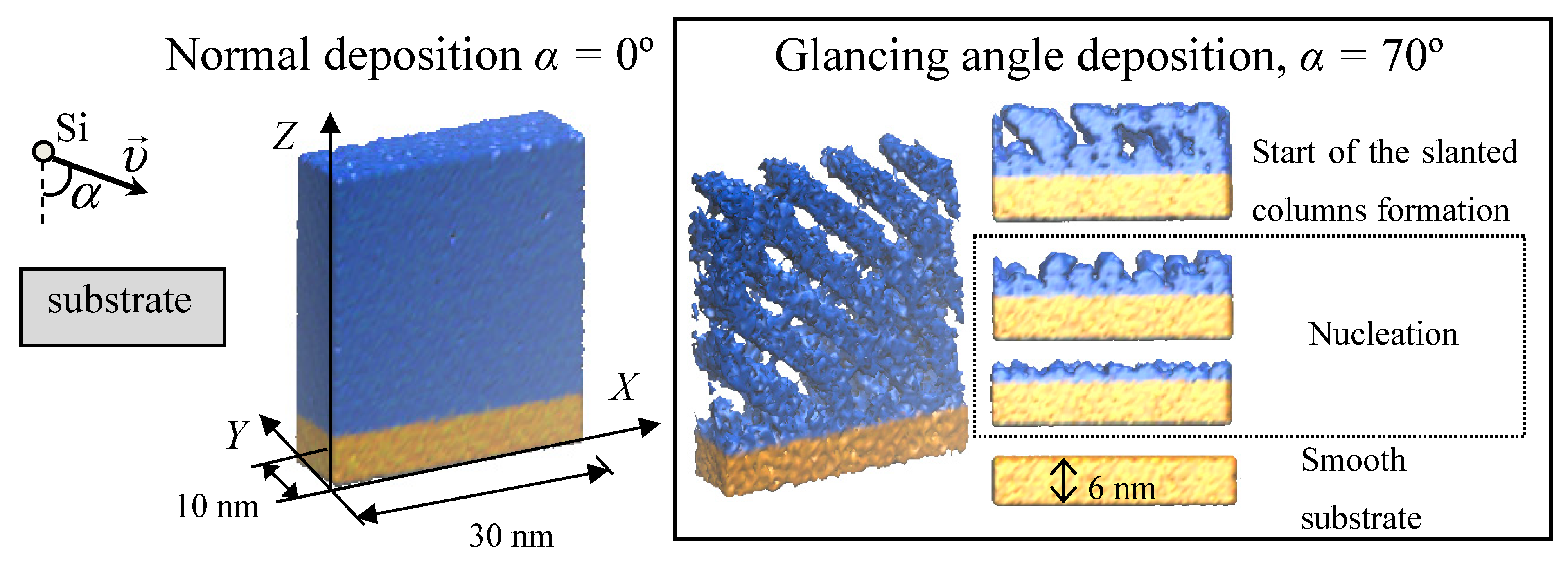
14]. Horizontal dimensions of substrate clusters were equal to 10 and 30 nm, the vertical dimension was equal to 6 nm. Horizontal dimensions of the cluster in the simulation of film deposition were the same as those of the substrate.
Choice of the deposition angle.
Simulation of the silicon dioxide film deposition as described above. The number of injection steps was Ns = 250. This ensured the growth of layer with a thickness of approximately 2.5 nm. During the simulation, it was revealed that at the initial stage of the film growth, the absolute value of the stress rapidly increased with increasing film thickness. To take this into account, Ns was reduced to 100 if the film thickness was less than 10 nm.
Simulation of the deposited cluster in the NVT ensemble and calculation of the pressure tensor components
pxx(yy). The initial state for the simulation was the final state after the completion of
Ns injection steps. The length of the MD trajectory for averaging of
pxx(yy) values was taken equal to 100 ps [
15]. The stress tensor components were calculated as shown in
Figure 1, where
L and
H are the vertical dimensions of the simulation box and film thickness, respectively. The multiplier (
L/
H) in the equation of
Figure 1 ensured the correction of pressure to the empty volume at the top part of the box [
18].
Stages 3–4 were repeated until the film thickness achieved a specified value of about 40 nm. This required approximately 4000 injection steps. The initial state for the simulation was the final state of stage 4. The total number of atoms in the final cluster was about one million.
MD simulation was performed using the GROMACS package [
19]. Components of the pressure tensor were calculated as follows [
19]:
where
V is the volume of the simulation box,
and
are the kinetic energy and virial tensors, respectively:
Here,
means the direct product of two vectors. The same expression was used for the pressure and stress calculations in MD modeling in [
20].
In the above scheme, the simulation with constant volume in step 4 takes into account the effect of the substrate on the film. Maintaining a constant volume leads to the appearance of stresses in the deposited films. These stresses were compensated by the external pressure applied to the boundaries of the simulation box, perpendicular to the substrate plane. Values of the pressure tensor components were not specified “by hand” but were calculated using Equations (1) and (2) from MD trajectories. Thus, the horizontal stress tensor components can be defined through the corresponding pressure tensor components. In the vertical direction, stress was absent since the gas phase (
Figure 1) did not prevent the film expansion.
For visual analysis of the atomistic structures, the visual molecular dynamic (VMD) package was used [
21]. The simulation was carried out using equipment at the shared research facilities of the high performance computing resources at Lomonosov Moscow State University [
22].
3. Results and Discussion
Initial values of the deposited Si atom’s velocities were specified as in our previous work [
23]:
where α is the deposition angle (see
Figure 2, left side) and
υ0 corresponds to the initial kinetic energy of Si atoms,
E(Si) = 10 eV. The variation in velocity directions of oxygen atoms did not noticeably affect the properties of the deposited films. For this reason, the initial velocities of oxygen atoms were directed to the substrate perpendicular to its surface.
The differences in the structure of normally deposited films and GLAD films are shown in
Figure 2. In GLAD films, the flux fluctuations of incoming atoms resulted in the density fluctuations of the substrate surface. Due to the shadow effect [
3], these fluctuations became the nuclei of future slanted columns (
Figure 2, right side). The columnar structures were formed when the thickness of the film exceeded a few nanometers. The voids between the columns are a characteristic feature of the GLAD films [
3]. These voids lead to a decrease in the density and refractive index of GLAD films compared with corresponding values for the normally deposited films.
The stress tensor components were calculated for both normally deposited films and GLAD films.
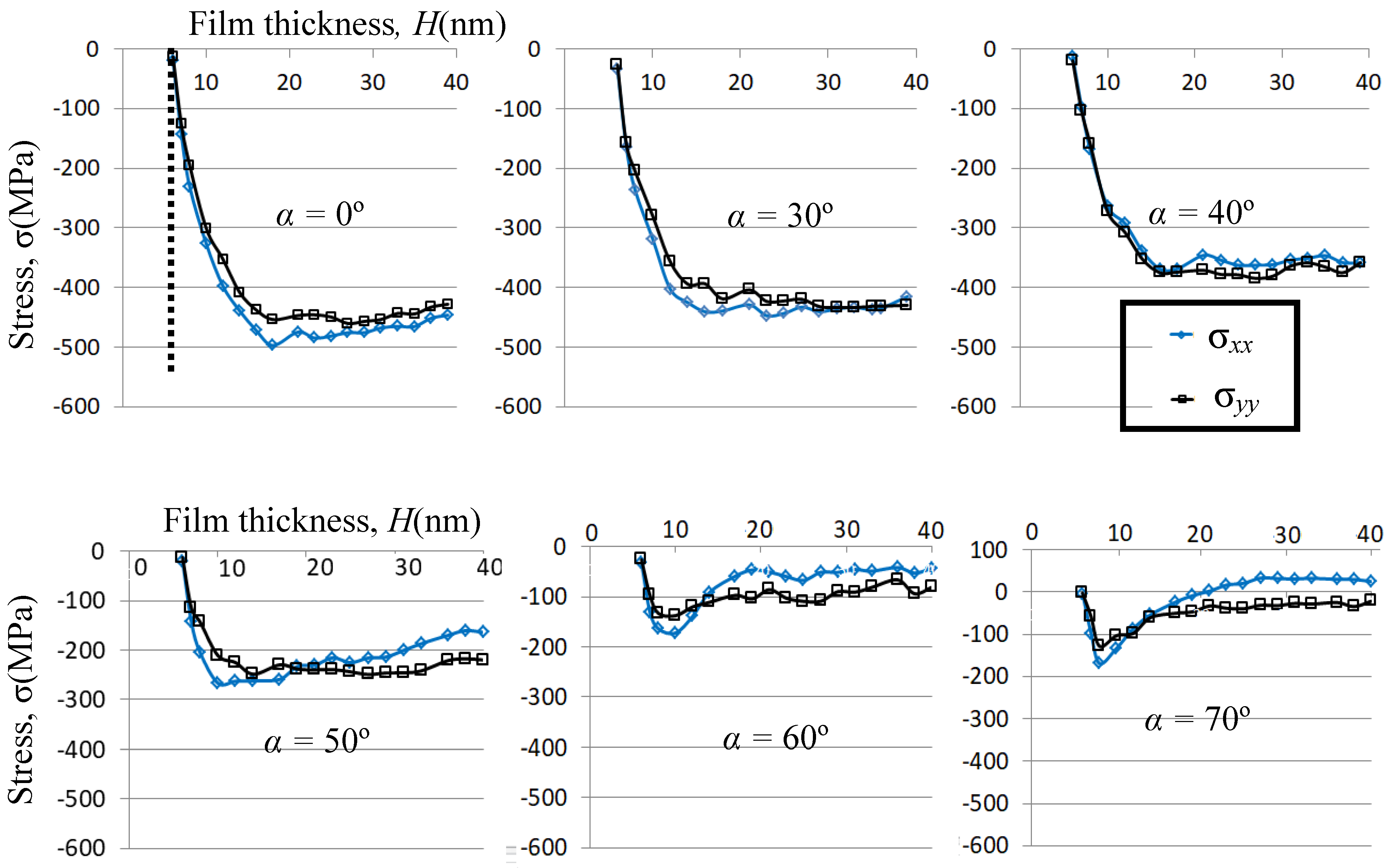
Results are shown in
Figure 3. A negative sign of the
σxx(yy) values means that the stress is compressive. Values of the off-diagonal components
σxy =
σyx and values of the root mean square deviation of the
σ are approximately several MPa. Thickness of the transition layer between substrate and film was about of 10 nm for the case of the normal deposition (top row in
Figure 3). Since the substrate was prepared using the NPT ensemble under the pressure of
P = 1 atm [
14], the values of the stress tensor components are close to zero for
H values smaller than the substrate thickness.
For all of the deposition angles, the initial stage of the film growth was accompanied by a sharp increase in the absolute values of
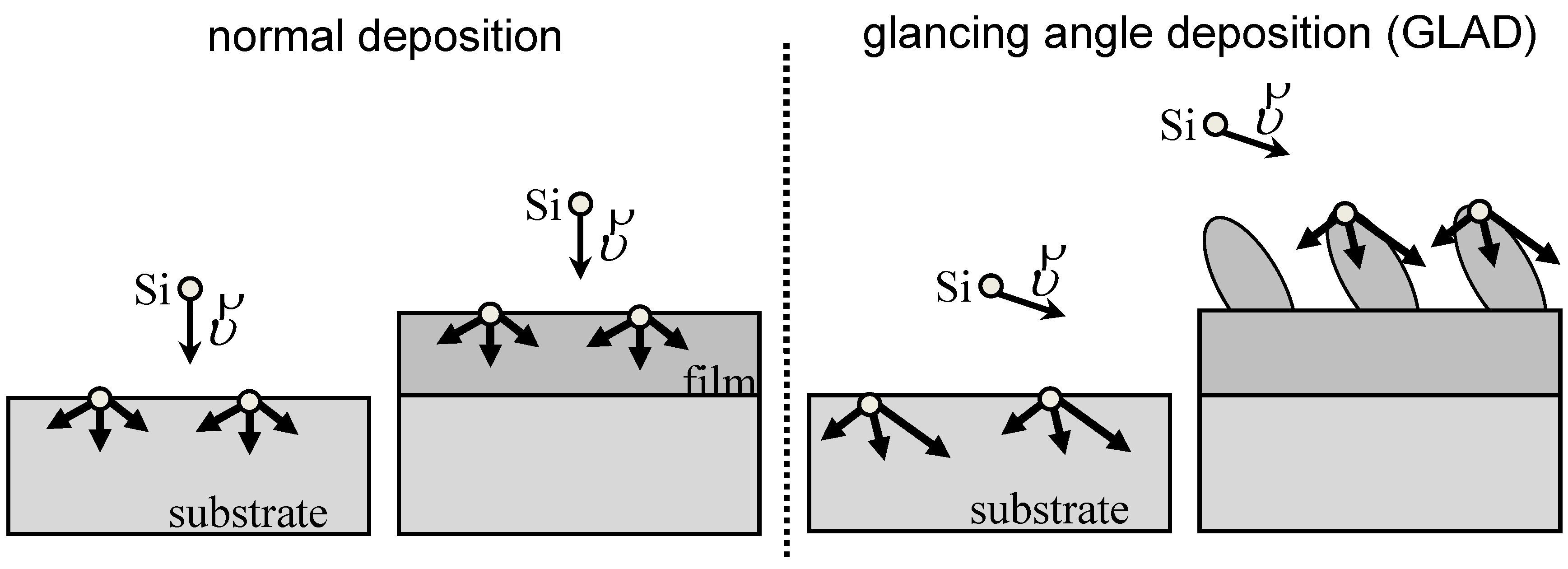
σxx(yy). This is because the high-energy silicon atoms push the substrate material away from the point of impact (black arrows in
Figure 4), which results in the increase of the pressure and stresses at the boundaries of the simulation box. Since the deposition started from the same substrate for all deposition angles, this effect appeared both for the normal deposition and for the glancing angle deposition. The resulting pressure growth correlated with a local densification of the GLAD films in the layer closest to the substrate. Density increased from the substrate value 2.2 g/cm
3 to approximately 2.4 g/cm
3, which corresponded to the density of the normally deposited films, and then decreased to a value of approximately 1.5 g/cm
3, corresponding to the averaged density of GLAD films.
With increase of the film thickness, a dependence of the structure on the deposition angle appeared. High-energy normal deposition produced a dense film and the local pressure appearing around the impact point was transmitted to the boundaries of the simulation box, just as in the initial stage of film growth. In contrast, glancing angle deposition resulted in the formation of a highly porous structure consisting of separate slanted columns (
Figure 4, right side). In this case, the pressure appearing around the impact point could be absorbed by voids between the columns. This is why the pressure transmitted to the boundaries was significantly lower than in the case of a normal deposition.
The described effect resulted in the differences of stress behavior for normal and GLAD films when film thickness
H exceeded approximately ten nanometers. For the case of normal deposition, absolute values of
σxx(yy) slightly decreased with growth of
H (top row in
Figure 3). The relative difference of stress tensor components |
σxx −
σyy|/|
σxx(yy)| << 1 for the cases of α = 0°, 30°, 40°. In contrast, in GLAD films (α = 60°, 70°), values of |
σxx(yy)| were essentially reduced with growth of film thickness. The parameter |
σxx −
σyy|/|
σxx(yy)|, characterizing the stress anisotropy, increased with growth of
H. It is explained by the anisotropy of the GLAD film’s structure in horizontal directions (right structure in
Figure 2). In the case of α = 50°,
σ(
H) dependencies show the intermediate behavior between normal deposition and glancing angle deposition.
The effect of substrate dimensions to stresses was also studied. Values of stresses in the films deposited under angles α = 0° and 70° on the substrate with horizontal dimensions of 20 × 60 nm and vertical dimension 6 nm were calculated. The corresponding atomistic clusters were obtained in our previous work [
23]. The deposition parameters, excluding cluster dimensions, were the same as those described in
Section 2. In the case of normal deposition (α = 0°), relative difference in stress values due to the difference in substrate dimensions was about 10%. In GLAD film (α = 70°), the maximum absolute stress values corresponded to a film thickness of about 10 nm and exceeded by approximately 1.5 times the stress values obtained for the same thickness of the film deposited on the 10 nm × 30 nm substrate (bottom row in
Figure 3). With growth of film thickness, the stress was reduced to almost the same value as shown in the right plots of the bottom row of
Figure 3.
Stresses were also calculated for the structures obtained in MD simulations of GLAD with the alternation of deposition angle and with substrate rotation at fixed α [
24]. The alternation means that the
υx in Equation (3) periodically changes sign. The rotation means that velocity components in Equation (3) change with time
t as follows:
υx =
υ0sn(α)sn(ω
t) and
υy =
υ0sn(α)cos(ω
t), where ω is rotation speed [
24]. The type of growing-film structure, chevron-like or tree-like, depended on the relationships between the alternation period and the rate of film growth. Chevron-like structures and tree-like structures were characterized by compressive stress values of about –(20 ÷ 40) MPa. In contrast, the tensile stress of about 20 MPa was obtained for the helical structure.
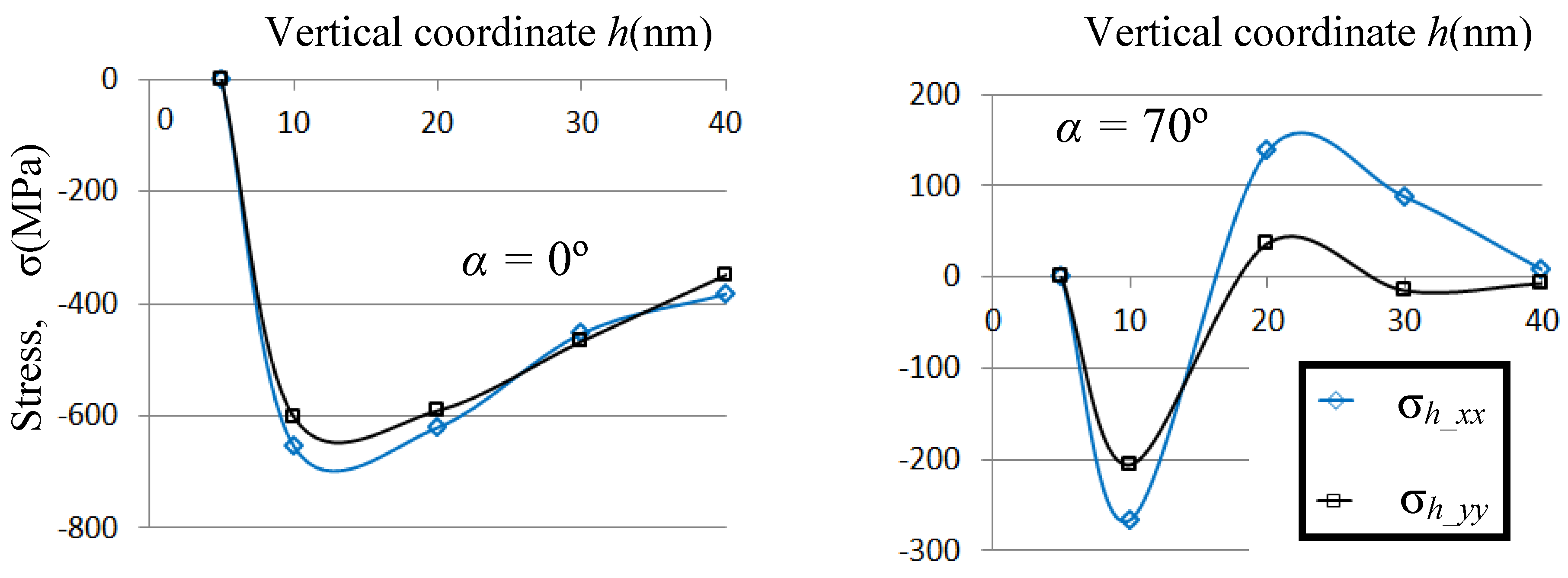
The stress distribution functions
σh_xx(yy)(
h) along the vertical coordinate
h were determined through the derivative of the product of averaged stresses
σxx(yy) and film thickness with respect to the vertical coordinate [
2]. We assumed that the stress does not change after deposition. The calculated values of
σh_xx(yy)(
h) were averaged over an interval of 10 nm to smooth out fluctuations arising from differentiation. Results are presented in
Figure 5. Stress components in the normally deposited films were compressive for all values of vertical coordinate. Their absolute values decreased when the value of
h exceeded 20 nm. For GLAD film, stresses were compressive when the vertical coordinate
h was less than 15 nm. Then the stress changed sign and became tensile. The absolute values of
σh_xx(yy)(
h) decreased with increasing vertical coordinate when
h exceeded 20 nm.
Our results of the stress calculations were compared with the available experimental data obtained by other research groups. They found a decrease in stress values with increasing deposition angle (
Figure 3), which was previously reported for different films deposited by magnetron sputtering [
25]. The absolute value of the compressive stress in a normally deposited film (upper row in
Figure 3) was in the range of experimental data [
1,
2,
26]. The change of stress from compressive to tensile with the growth of deposition angle was observed experimentally for the silicon dioxide films fabricated by electron beam evaporation [
27]. Such a change was detected in our simulation (see results for α = 70° in
Figure 3). Since the electron beam evaporation is a low-energetic process, the experimental stress values in [
27] were lower than those obtained in our simulation. A change in the sign of stress with an increase in the deposition angle was also found for GLAD diamond-like carbon films [
7] and hafnium nitride films [
28]. Thus, the simulation results we obtained are in good qualitative agreement with previously reported experimental results.
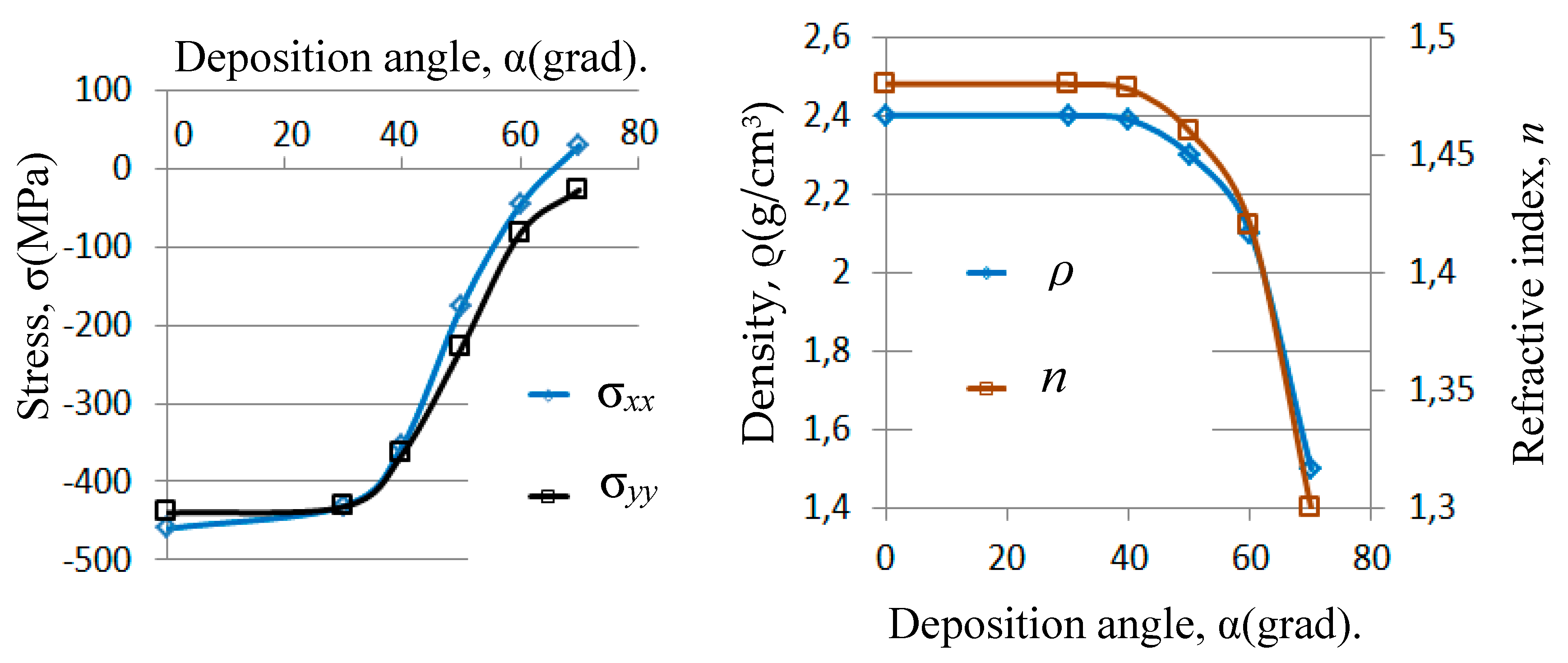
The dependencies of stress, density, and refractive index on the deposition angle are shown in
Figure 6. These dependencies were obtained by averaging of the respective parameters over the volume, from
H = 30 nm to
H = 40 nm.
Refractive index
n was calculated using the Maxwell relation between refractive index and dielectric constant
n2 =
ε and Bruggeman effective medium theory [
29] for the porous films [
9]:
where
f1 is the void volume fraction, ε
1 is the dielectric constant of dense film fraction, ε is the effective dielectric constant. Refractive index of dense silicon dioxide film deposited on fused silica by the IBS process is equal to 1.48 (632 nm) [
30], so ε
1 = 2.19. Dependence of
f1 on the deposition angle α is defined as follows:
where
V1(α) and
V (α) are the void volume and the total film volume, respectively, ρ(α) is the film density averaged over the volume from
H = 30 nm to
H = 40 nm, ρ(0) = 2.4 g/cm
3 is the density of the normally deposited film. It was assumed that the normally deposited film has no free volume and the density inside the slanted columns of GLAD films was equal to ρ(0). Refractive index was calculated as
n = √
ε and its dependence on α was found by using Equations (4) and (5).
As expected, the refractive index decreased with growth of the deposition angle, which correlates with the decrease of the stress tensor components. The density dependence on the deposition angle agreed with the earlier reported results of the atomistic simulation using the ballistic approach [
11]. The films with low refractive index,
n = 1.32 (α =70°), were characterized by low values of both stress tensor components. Values of the refractive index for large deposition angles were in the interval of the experimental results for SiO
2 GLAD films [
31].

