High-Power GaN-Based Vertical Light-Emitting Diodes on 4-Inch Silicon Substrate

 ,
,
Abstract
1. Introduction
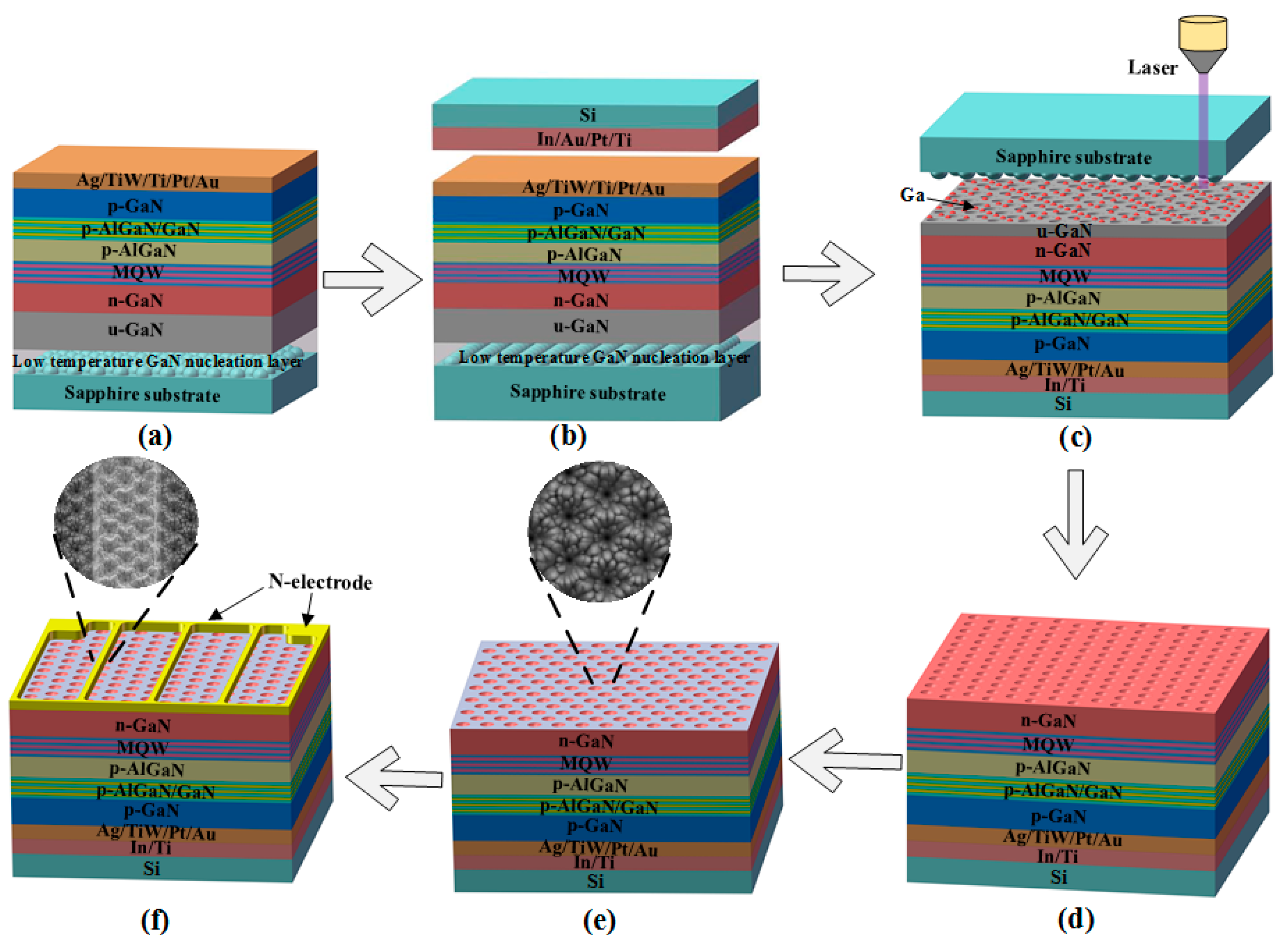
2. Experiments
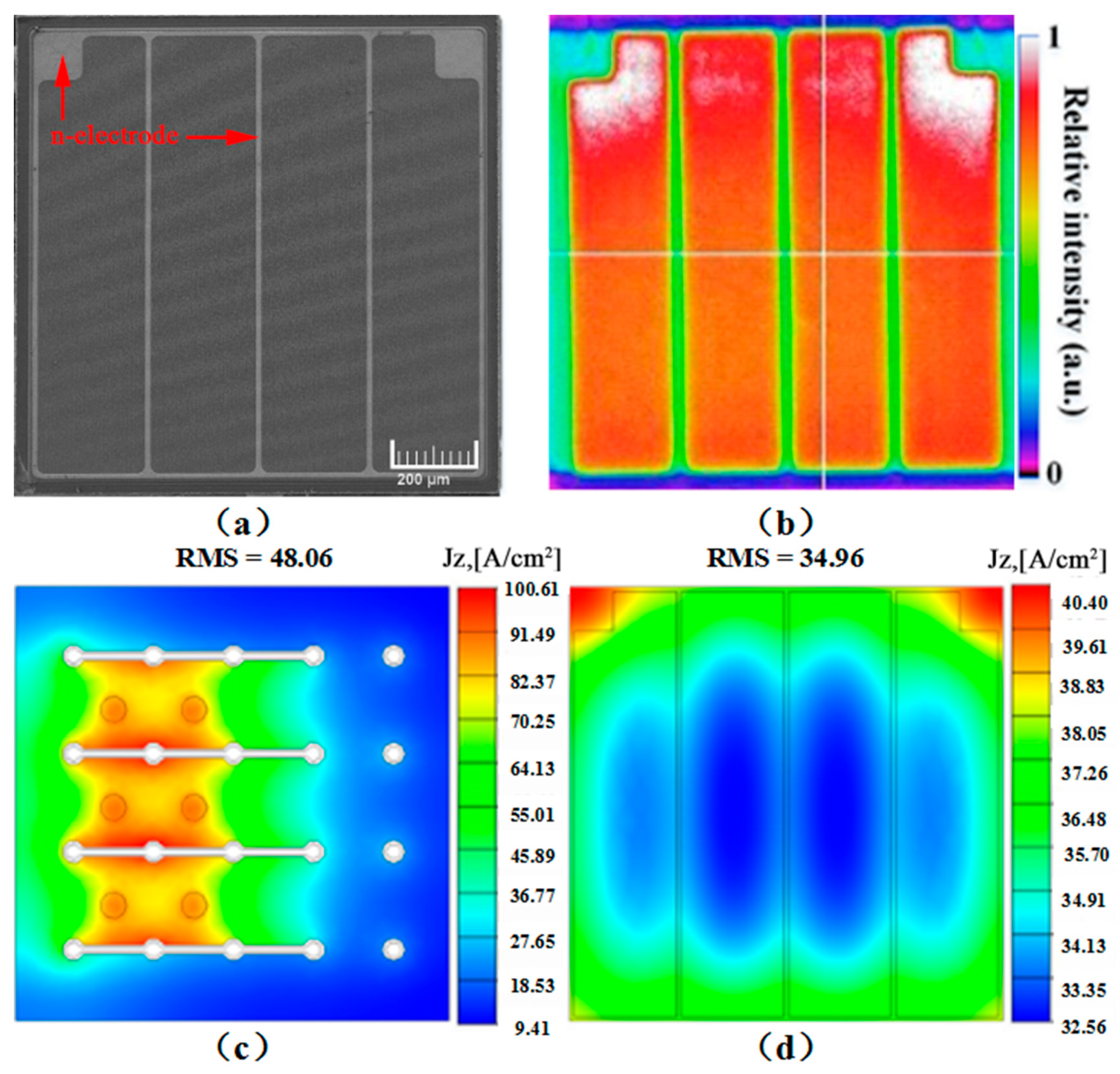
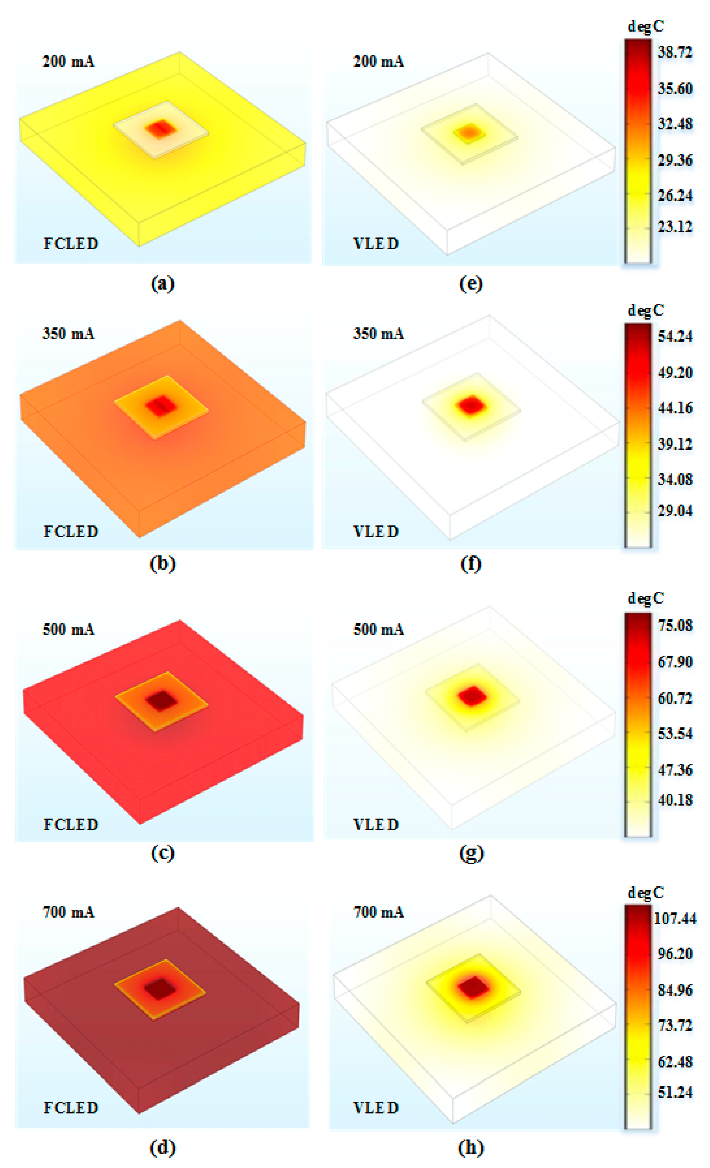
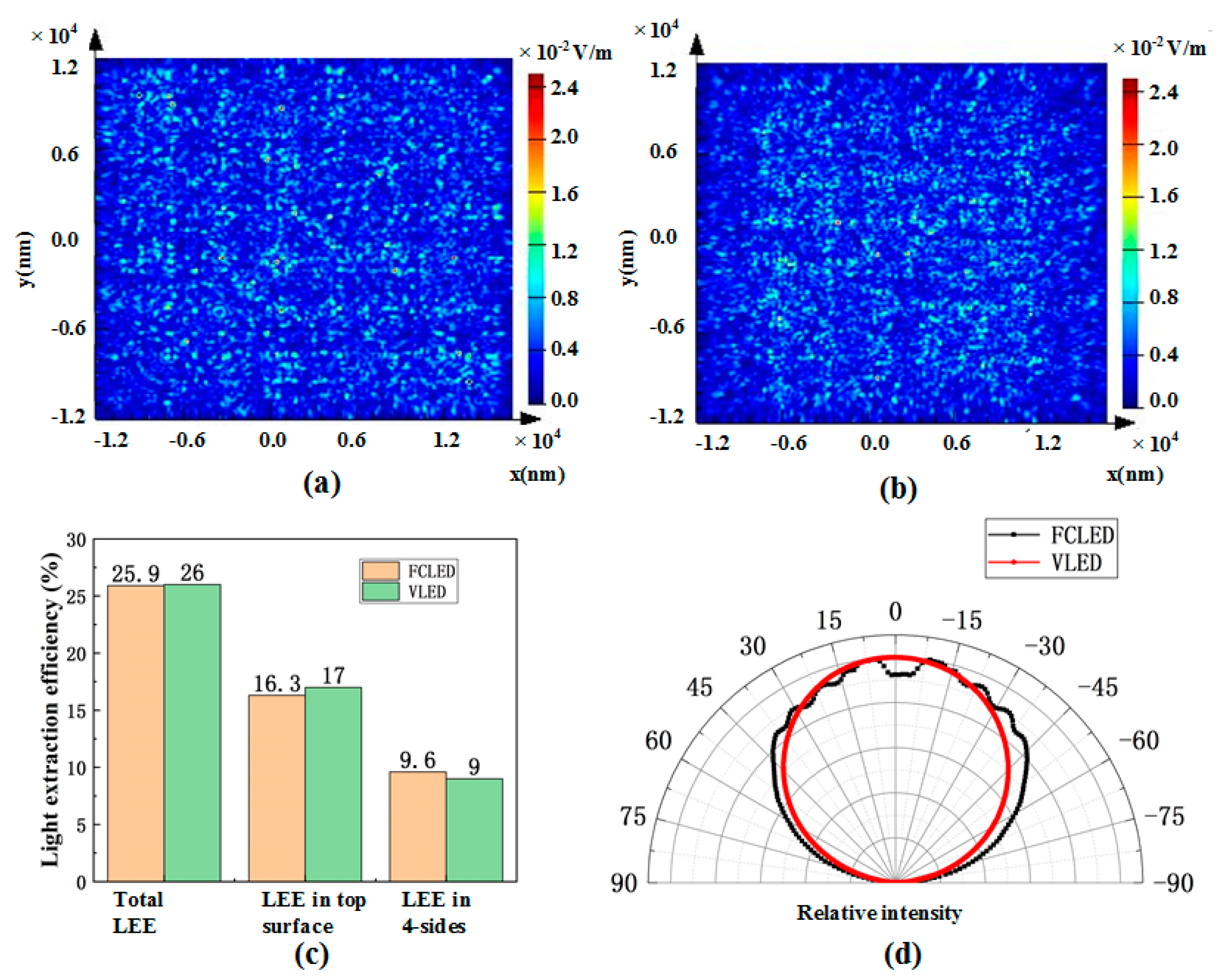
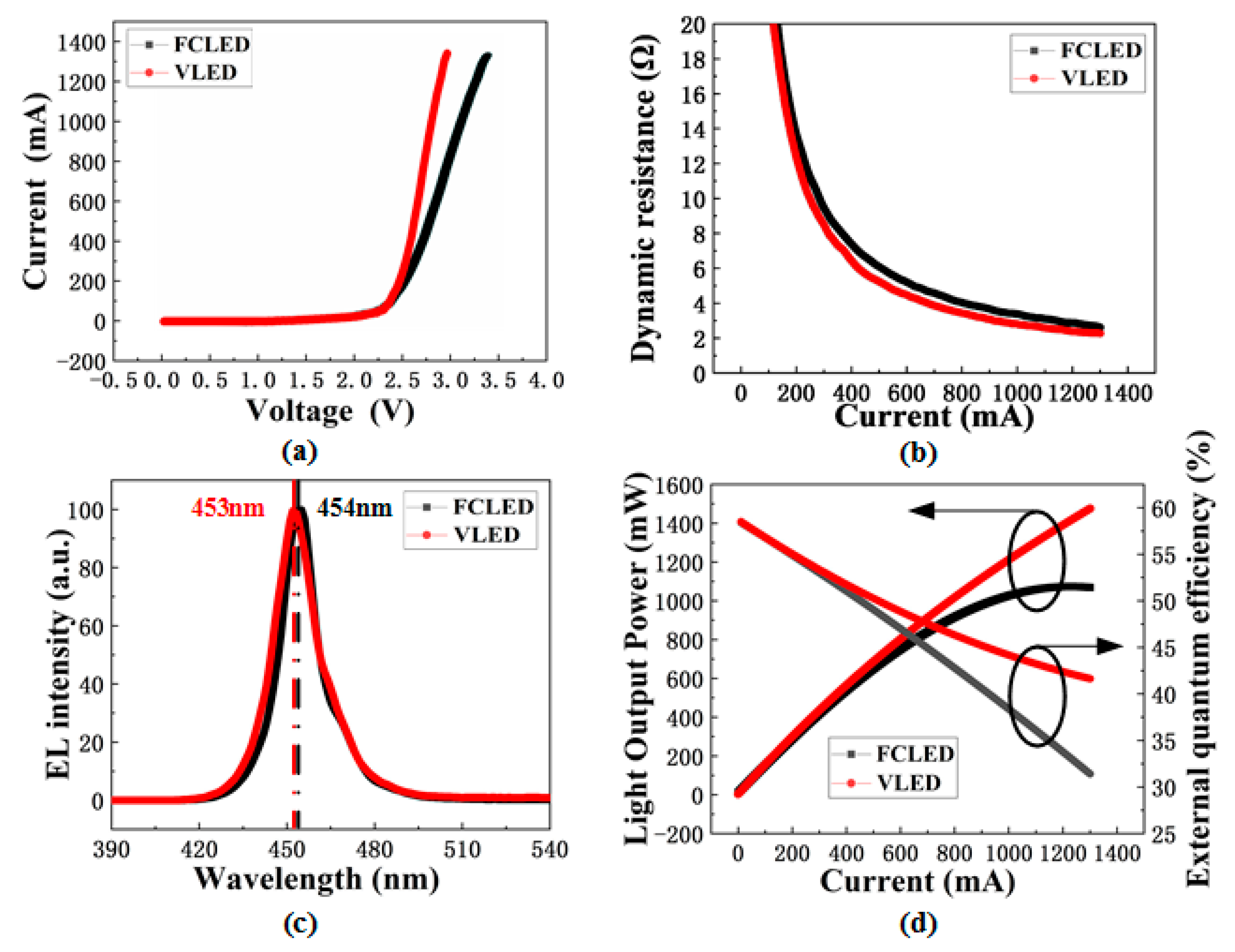
3. Results and Discussion
4. Conclusions
Author Contributions
Funding
Conflicts of Interest
References
- Wierer, J.J., Jr.; David, A.; Megens, M.M. III-nitride photonic-crystal light-emitting diodes with high extraction efficiency. Nat. Photonics 2009, 3, 163–169. [Google Scholar] [CrossRef]
- Tang, B.; Miao, J.; Liu, Y.; Wan, H.; Li, N.; Zhou, S.; Gui, C. Enhanced Light Extraction of Flip-Chip Mini-LEDs with Prism-Structured Sidewall. Nanomaterials 2019, 9, 319. [Google Scholar] [CrossRef] [PubMed]
- Sadaf, S.M.; Ra, Y.H.; Szkopek, T.; Mi, Z. Monolithically Integrated Metal/Semiconductor Tunnel Junction Nanowire Light-Emitting Diodes. Nano Lett. 2016, 16, 1076–1080. [Google Scholar] [CrossRef] [PubMed]
- Rae, K.; Foucher, C.; Guilhabert, B.; Islim, M.S.; Yin, L.; Zhu, D.; Oliver, R.A.; Wallis, D.J.; Haas, H.; Laurand, N. InGaN µLEDs integrated onto colloidal quantum dot functionalized ultra-thin glass. Opt. Express 2017, 25, 19179–19184. [Google Scholar] [CrossRef] [PubMed]
- Wei, T.; Huo, Z.; Zhang, Y.; Zheng, H.; Chen, Y.; Yang, J.; Hu, Q.; Duan, R.; Wang, J.; Zeng, Y. Efficiency enhancement of homoepitaxial InGaN/GaN light-emitting diodes on free-standing GaN substrate with double embedded SiO2 photonic crystals. Opt. Express 2014, 22, A1093–A1100. [Google Scholar] [CrossRef]
- Hu, H.; Zhou, S.; Liu, X.; Gao, Y.; Gui, C.; Liu, S. Effects of GaN/AlGaN/Sputtered AlN nucleation layers on performance of GaN-based ultraviolet light-emitting diodes. Sci. Rep. 2017, 7, 44627. [Google Scholar] [CrossRef] [PubMed]
- Zhou, S.; Xu, H.; Hu, H.; Gui, C.; Liu, S. High quality GaN buffer layer by isoelectronic doping and its application to 365 nm InGaN/AlGaN ultraviolet light-emitting diodes. Appl. Surf. Sci. 2019, 471, 231–238. [Google Scholar] [CrossRef]
- Piprek, J. Efficiency droop in nitride-based light-emitting diodes. Phys. Status Solidi 2010, 207, 2217–2225. [Google Scholar] [CrossRef]
- Oh, S.H.; Lee, T.H.; Son, K.R.; Kim, T.G. Fabrication of HfO2/TiO2–based conductive distributed Bragg reflectors: Its application to GaN-based near-ultraviolet micro-light emitting diodes. J. Alloys Compd. 2019, 773, 490–495. [Google Scholar] [CrossRef]
- Meyaard, D.S.; Shan, Q.; Cho, J.; Schubert, E.F.; Han, S.H.; Kim, M.H.; Sone, C.; Oh, S.J.; Kim, J.K. Temperature dependent efficiency droop in GaInN light-emitting diodes with different current densities. Appl. Phys. Lett. 2012, 100, 081106. [Google Scholar] [CrossRef]
- Zhou, S.; Wang, S.; Liu, S.; Ding, H. High power GaN-based LEDs with low optical loss electrode structure. Opt. Laser Technol. 2013, 54, 321–325. [Google Scholar] [CrossRef]
- Zhou, S.; Liu, X.; Yan, H.; Chen, Z.; Liu, Y.; Liu, S. Highly efficient GaN-based high-power flip-chip light-emitting diodes. Opt. Express 2019, 27, A669–A692. [Google Scholar] [CrossRef]
- Xu, J.; Zhang, W.; Peng, M.; Dai, J.; Chen, C. Light-extraction enhancement of GaN-based 395 nm flip-chip light-emitting diodes by an Al-doped ITO transparent conductive electrode. Opt. Lett. 2018, 43, 2684–2687. [Google Scholar] [CrossRef]
- Han, N.; Cuong, T.V.; Han, M.; Ryu, B.D.; Chandramohan, S.; Park, J.B.; Kang, J.H.; Park, Y.J.; Ko, K.B.; Kim, H.Y. Improved heat dissipation in gallium nitride light-emitting diodes with embedded graphene oxide pattern. Nat. Commun. 2013, 4, 1452. [Google Scholar] [CrossRef]
- Zhou, S.; Zheng, C.; Lv, J.; Gao, Y.; Wang, R.; Liu, S. GaN-based flip-chip LEDs with highly reflective ITO/DBR p-type and via hole-based n-type contacts for enhanced current spreading and light extraction. Opt. Laser Technol. 2017, 92, 95–100. [Google Scholar] [CrossRef]
- Lv, J.; Zheng, C.; Chen, Q.; Zhou, S.; Liu, S. High power InGaN/GaN flip-chip LEDs with via-hole-based two-level metallization electrodes. Phys. Status Solidi A 2016, 213, 3150–3156. [Google Scholar] [CrossRef]
- Ha, J.S.; Lee, S.W.; Lee, H.J.; Lee, H.J.; Lee, S.H.; Goto, H.; Kato, T.; Fujii, K.; Cho, M.W.; Yao, T. The fabrication of vertical light-emitting diodes using chemical lift-off process. IEEE Photonics Technol. Lett. 2008, 20, 175–177. [Google Scholar] [CrossRef]
- Yum, W.S.; Song, J.O.; Jeong, H.H.; Oh, J.T.; Seong, T.Y. Improving performance of high-power indium gallium nitride/gallium nitride-based vertical light-emitting diodes by employing simple n-type electrode pattern. Mater. Sci. Semicond. Process. 2015, 31, 209–213. [Google Scholar] [CrossRef]
- Cao, X.A.; Arthur, S.D. High-power and reliable operation of vertical light-emitting diodes on bulk GaN. Appl. Phys. Lett. 2004, 85, 3971–3973. [Google Scholar] [CrossRef]
- Liu, L.; Yin, L.; Teng, D.; Zhang, J.; Ma, X.; Wang, G. An explanation for catastrophic failures of GaN-based vertical structure LEDs subjected to thermoelectric stressing. J. Phys. D Appl. Phys. 2015, 48, 305102. [Google Scholar] [CrossRef]
- Liu, L.; Ling, M.; Yang, J.; Xiong, W.; Jia, W.; Wang, G. Efficiency degradation behaviors of current/thermal co-stressed GaN-based blue light emitting diodes with vertical-structure. J. Appl. Phys. 2012, 111, 093110. [Google Scholar] [CrossRef]
- Oh, J.T.; Moon, Y.T.; Kang, D.S.; Park, C.K.; Han, J.W.; Jung, M.H.; Sung, Y.J.; Jeong, H.H.; Song, J.O.; Seong, T.Y. High efficiency ultraviolet GaN-based vertical light emitting diodes on 6-inch sapphire substrate using ex-situ sputtered AlN nucleation layer. Opt. Express 2018, 26, 5111–5117. [Google Scholar] [CrossRef]
- Li, C.K.; Wu, Y.R. Study on the Current Spreading Effect and Light Extraction Enhancement of Vertical GaN/InGaN LEDs. IEEE Trans. Electron Devices 2012, 59, 400–407. [Google Scholar] [CrossRef]
- Wu, F.L.; Ou, S.L.; Kao, Y.C.; Chen, C.L.; Tseng, M.C.; Lu, F.C.; Lin, M.T.; Horng, R.H. Thin-film vertical-type AlGaInP LEDs fabricated by epitaxial lift-off process via the patterned design of Cu substrate. Opt. Express 2015, 23, 18156–18165. [Google Scholar] [CrossRef]
- Tan, B.S.; Yuan, S.; Kang, X.J. Performance enhancement of InGaN light-emitting diodes by laser lift-off and transfer from sapphire to copper substrate. Appl. Phys. Lett. 2004, 84, 2757–2759. [Google Scholar] [CrossRef]
- Lin, W.Y.; Wuu, D.S.; Pan, K.F.; Huang, S.H.; Lee, C.E.; Wang, W.K.; Hsu, S.C.; Su, Y.Y.; Huang, S.Y.; Horng, R.H. High-power GaN-mirror-Cu light-emitting diodes for vertical current injection using laser liftoff and electroplating techniques. IEEE Photonics Technol. Lett. 2005, 17, 1809–1811. [Google Scholar] [CrossRef]
- Doan, T.; Tran, C.; Chu, C.; Chen, C.; Liu, W.H.; Chu, J.; Yen, K.; Chen, H.; Fan, F. Vertical GaN based light emitting diodes on metal alloy substrate boosts high power LED performance. In Proceedings of SPIE—The International Society for Optical Engineering; Society of Photo-Optical Instrumentation Engineers: Bellingham, WA, USA, 2007; Volume 6669. [Google Scholar]
- Tran, C.A.; Chu, C.F.; Cheng, C.C.; Liu, W.H.; Chu, J.Y.; Cheng, H.C.; Fan, F.H.; Yen, J.K.; Doan, T. High brightness GaN vertical light emitting diodes on metal alloyed substrate for general lighting application. J. Cryst. Growth 2007, 298, 722–724. [Google Scholar] [CrossRef]
- Chu, C.F.; Cheng, C.C.; Liu, W.H.; Chu, J.Y.; Fan, F.H.; Cheng, H.C.; Doan, T.; Tran, C.A. High Brightness GaN Vertical Light-Emitting Diodes on Metal Alloy for General Lighting Application. Proc. IEEE 2010, 98, 1197–1207. [Google Scholar]
- Wong, W.S.; Wengrow, A.B.; Cho, Y.; Salleo, A.; Quitoriano, N.J.; Cheung, N.W.; Sands, T. Integration of GaN thin films with dissimilar substrate materials by Pd-In metal bonding and laser lift-off. J. Electron. Mater. 1999, 28, 1409–1413. [Google Scholar] [CrossRef]
- Liu, W.J.; Hu, X.L.; Zhang, J.Y.; Weng, G.E.; Lv, X.Q.; Huang, H.J.; Chen, M.; Cai, X.M.; Ying, L.Y.; Zhang, B.P. Low-temperature bonding technique for fabrication of high-power GaN-based blue vertical light-emitting diodes. Opt. Mater. 2012, 34, 1327–1329. [Google Scholar] [CrossRef]
- Lee, S.Y.; Choi, K.K.; Jeong, H.H.; Choi, H.S.; Oh, T.H.; Song, J.O.; Seong, T.Y. Wafer-level fabrication of GaN-based vertical light-emitting diodes using a multi-functional bonding material system. Semicond. Sci. Technol. 2009, 24, 092001. [Google Scholar] [CrossRef]
- Zhou, S.; Liu, X.; Gao, Y.; Liu, Y.; Liu, M.; Liu, Z.; Gui, C.; Liu, S. Numerical and experimental investigation of GaN-based flip-chip light-emitting diodes with highly reflective Ag/TiW and ITO/DBR Ohmic contacts. Opt. Express 2017, 25, 26615–26627. [Google Scholar] [CrossRef]
- Mion, C. Investigation of the Thermal Properties of Gallium Nitride Using the Three Omega Technique. Ph.D. Thesis, North Carolina State University, Raleigh, NC, USA, 2006. [Google Scholar]


| Current | 200 mA | 350 mA | 500 mA | 700 mA | ||||
|---|---|---|---|---|---|---|---|---|
| LED Type | FCLED | VLED | FCLED | VLED | FCLED | VLED | FCLED | VLED |
| Maximum current density (A/cm2) | 56.41 | 22.76 | 100.61 | 49.29 | 146.13 | 58.15 | 211.05 | 82.13 |
| Minimum current density (A/cm2) | 6.18 | 18.84 | 9.41 | 32.66 | 12.5 | 46.40 | 16.38 | 64.62 |
| Root mean square (RMS) value (A/cm2) | 27.37 | 19.99 | 48.06 | 34.96 | 68.95 | 34.93 | 97.93 | 49.92 |
| Current | 200 mA | 350 mA | 500 mA | 700 mA | ||||
|---|---|---|---|---|---|---|---|---|
| LED Type | FCLED | VLED | FCLED | VLED | FCLED | VLED | FCLED | VLED |
| Maximum temperature (°C) | 35.90 | 31.78 | 53.71 | 44.83 | 74.52 | 59.90 | 107.41 | 83.11 |
| Minimum temperature (°C) | 35.76 | 31.75 | 53.41 | 44.77 | 74.05 | 59.79 | 106.64 | 82.94 |
© 2019 by the authors. Licensee MDPI, Basel, Switzerland. This article is an open access article distributed under the terms and conditions of the Creative Commons Attribution (CC BY) license (http://creativecommons.org/licenses/by/4.0/).
Share and Cite
Zhao, Q.; Miao, J.; Zhou, S.; Gui, C.; Tang, B.; Liu, M.; Wan, H.; Hu, J. High-Power GaN-Based Vertical Light-Emitting Diodes on 4-Inch Silicon Substrate. Nanomaterials 2019, 9, 1178. https://doi.org/10.3390/nano9081178
Zhao Q, Miao J, Zhou S, Gui C, Tang B, Liu M, Wan H, Hu J. High-Power GaN-Based Vertical Light-Emitting Diodes on 4-Inch Silicon Substrate. Nanomaterials. 2019; 9(8):1178. https://doi.org/10.3390/nano9081178
Chicago/Turabian StyleZhao, Qiang, Jiahao Miao, Shengjun Zhou, Chengqun Gui, Bin Tang, Mengling Liu, Hui Wan, and Jinfeng Hu. 2019. "High-Power GaN-Based Vertical Light-Emitting Diodes on 4-Inch Silicon Substrate" Nanomaterials 9, no. 8: 1178. https://doi.org/10.3390/nano9081178
APA StyleZhao, Q., Miao, J., Zhou, S., Gui, C., Tang, B., Liu, M., Wan, H., & Hu, J. (2019). High-Power GaN-Based Vertical Light-Emitting Diodes on 4-Inch Silicon Substrate. Nanomaterials, 9(8), 1178. https://doi.org/10.3390/nano9081178