Article

Properties-Adjustable Alumina-Zirconia Nanolaminate Dielectric Fabricated by Spin-Coating

1
School of Electronic and Information Engineering, South China University of Technology, Guangzhou 510640, China
2
Institute of Polymer Optoelectronic Materials and Devices, State Key Laboratory of Luminescent Materials and Devices, South China University of Technology, Guangzhou 510640, China
3
Key Laboratory of Advanced Display and System Applications of Ministry of Education, Shanghai University, Shanghai 200072, China
4
Institute for Advanced Materials and Guangdong Provincial Key Laboratory of Quantum Engineering and Quantum Materials, South China Normal University, Guangzhou 510006, China
*
Authors to whom correspondence should be addressed.
Nanomaterials 2017, 7(12), 419; https://doi.org/10.3390/nano7120419
Submission received: 15 October 2017 / Revised: 26 November 2017 / Accepted: 27 November 2017 / Published: 29 November 2017
(This article belongs to the Special Issue Mechanics, Electrical and Optical Properties of Nano-Thin Films)

Abstract

:
In this paper, an alumina-zirconia (Al2O3-ZrO2) nanolaminate dielectric was fabricated by spin-coating and the performance was investigated. It was found that the properties of the dielectric can be adjusted by changing the content of Al2O3/ZrO2 in nanolaminates: when the content of Al2O3 was higher than 50%, the properties of nanolaminates, such as the optical energy gap, dielectric strength (Vds), capacitance density, and relative permittivity were relatively stable, while the change of these properties became larger when the content of Al2O3 was less than 50%. With the content of ZrO2 varying from 50% to 100%, the variation of these properties was up to 0.482 eV, 2.12 MV/cm, 135.35 nF/cm2, and 11.64, respectively. Furthermore, it was demonstrated that the dielectric strength of nanolaminates were influenced significantly by the number (n) of bilayers. Every increment of one Al2O3-ZrO2 bilayer will enhance the dielectric strength by around 0.39 MV/cm (Vds ≈ 0.86 + 0.39n). This could be contributed to the amorphous alumina which interrupted the grain boundaries of zirconia.

1. Introduction

Oxide thin film transistors (TFTs) have attracted considerable interest because of their high-performance. In addition to oxide semiconductors, which were mostly investigated in the last few decades, the metal oxide dielectric plays an important role in the performance of TFTs. In recent years, as a novel structure of dielectrics, a nanolaminate dielectric has been studied and applied widely in optoelectronic devices [1,2]. Waggoner et al. found that nanolaminates can take advantage of different components thereby enhancing the performance and stability of the devices compared to single-layer dielectrics [2]. López et al. demonstrated that the optical properties of dielectrics can be modulated by varying the nanolaminate’s thickness [3]. The TiOx and AlOx nanolaminate dielectric has been applied in organic devices as moisture barriers by Nehm et al., and it is helpful to delay the degradation of OLEDs which was caused by moisture erosion [4]. Meanwhile, so many techniques have been developed to fabricate nanolaminate dielectrics, such as atomic layer deposition (ALD) [5], pulsed plasma-enhanced chemical vapor deposition [6], and cyclic chemical vapor deposition (CVD) [7]. However, the application of solution-process to fabricate nanolaminates were rarely reported, especially for spin-coating. Spin-coating has attracted more and more attention for low cost, simplicity, and high throughput [8]. Metal oxide dielectrics, such as Al2O3, HfO2, and ZrO2 can be obtained easily by spin-coating [9,10,11]. Meanwhile, it has the potential to realize fully transparent, flexible, and portable electronics [12,13].
In this work, we fabricated a series of nanolaminate dielectrics by spin-coating and the relevant structures and properties were investigated. Nanolaminate dielectric was prepared in two approaches: (1) changing the content of Al2O3 in nanolaminates with constant number of bilayers; and (2) changing the number of bilayers with a constant content of Al2O3. The results showed that the properties of the dielectric can be adjusted by controlling the content of the components in nanolaminates and the number of bilayers. It was demonstrated that the performance of nanolaminates fabricated by vacuum-process can also be realized in the solution process. Compared with the vacuum process, the nanolaminate dielectric fabricated by spin-coating succeeded in avoiding rigorous experimental conditions (such as a high ambient vacuum) and complex operation (such as controlling the deposition speed of the thin film) [2,14]. This paper provided a new idea to fabricate dielectrics by the solution process.

2. Materials and Methods

The precursor solution was prepared by dissolving ZrOCl2·8H2O and Al(NO3)3·9H2O in methoxyethanol, respectively. Substrates were cleaned by isopropanol, tetrahydrofuran, lotion, deionized water (twice), and isopropanol sequentially, and then dried at 80 °C in an oven. To activate the surface, substrates were treated by O2 atmospheric pressure plasma for 10 min [15]. The precursor was coated at 4000 rpm on substrate for 40 s and the resulting film was annealed in air for 1 h.
To find out the optimized annealing temperature for nanolaminate fabrication, ZrO2 and Al2O3 single layers were prepared. The resulting films were measured by X-ray reflectivity (XRR) to explore the relationship between thickness (as well as density) and annealing temperature. Then, the relationship between thickness and precursor concentration was also explored after the optimized temperature was confirmed. Finally, the results were analyzed by mathematical statistics and tested by Student’s t-test [16,17].
Al2O3-ZrO2 nanolaminates were fabricated by coating the precursor on substrate repeatedly, the resulting film will be annealed at optimized temperature for one hour in air before the next coating. The cross-sectional image of the nanolaminates is shown in Figure 1. The content of the components in the nanolaminates were controlled by the thickness ratio of Al2O3 (T1) and ZrO2 (T2). For example, if T1/T2 was 1:1 in bilayers, the content of Al2O3 was 50%. In this work, the content of Al2O3 was set to 0%, 25%, 50%, 75%, and 100%, and the number of bilayers was set to 1, 2, 3, and 6.
Crystallizations of the nanolaminate dielectric was identified by X-ray diffraction (XRD) at 40 kV and 40 mA, with Cu-kα used as X-ray source. The scanning was carried out at the rate of 0.1°/s from 20° to 70°. A UV-VIS spectrophotometer was used to characterize the transmittance of nanolaminates in a range from 200 nm to 800 nm and Eg can be obtained by the Tauc formula [18]. The microstructure of nanolaminates was analyzed by HR-TEM and EDS. The crystallite size of nanolaminates was calculated by Scherrer’s equation [19]:
D = k γ / Bcos θ
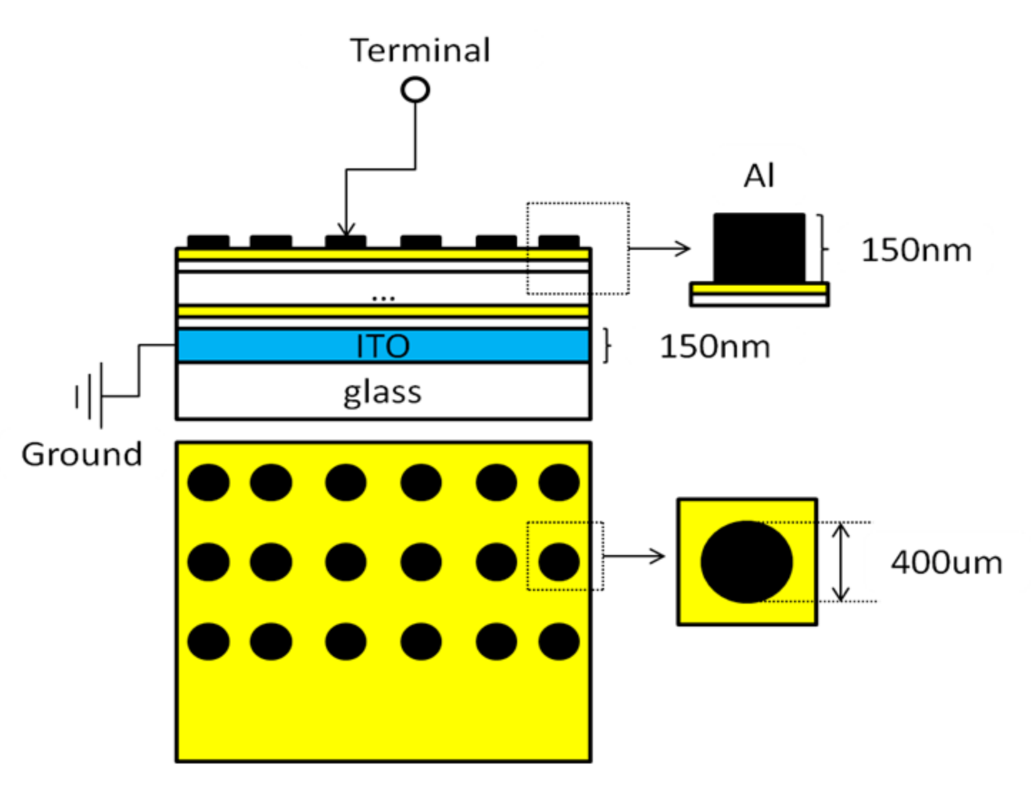
where D is the crystallite size, γ is the wavelength of X-ray (15.4056 nm), B is the full width at half maximum (FWHM), θ is the Bragg angle and k is the Scherrer constant (0.89). Substrates deposited with 150 nm indium tin oxide (ITO) were used to fabricate metal insulator metal (MIM) devices, as shown in Figure 2. ITO acts as the bottom electrode and top electrodes are prepared with aluminum (Al) deposited by an Edward Auto 500 unit. The diameter and thickness of Al electrodes are 400 μm and 150 nm, respectively. A semiconductor parameter analyzer was used to measure breakdown voltage under the direct current, the test voltage was applied from 0 V to 20 V with the step of 0.2 V. Vds was the value of breakdown voltage divided by electrode separation distance. Capacitance was measured by a Keithley4200-SCS unit. Meanwhile, relative permittivity ( ε r ) also can be calculated by the following formula [20]:
ε r =   C · d ε 0 · S   =   C · d ε 0 · π · r 2
where C, d, and S are the capacitance, thickness, and area of nanolaminates, respectively, and ε 0 = 8.854 × 10⁻¹² F/m (permittivity in free space).

3. Results and Discussion

3.1. Optimized Annealing Temperature Exploration and Verification

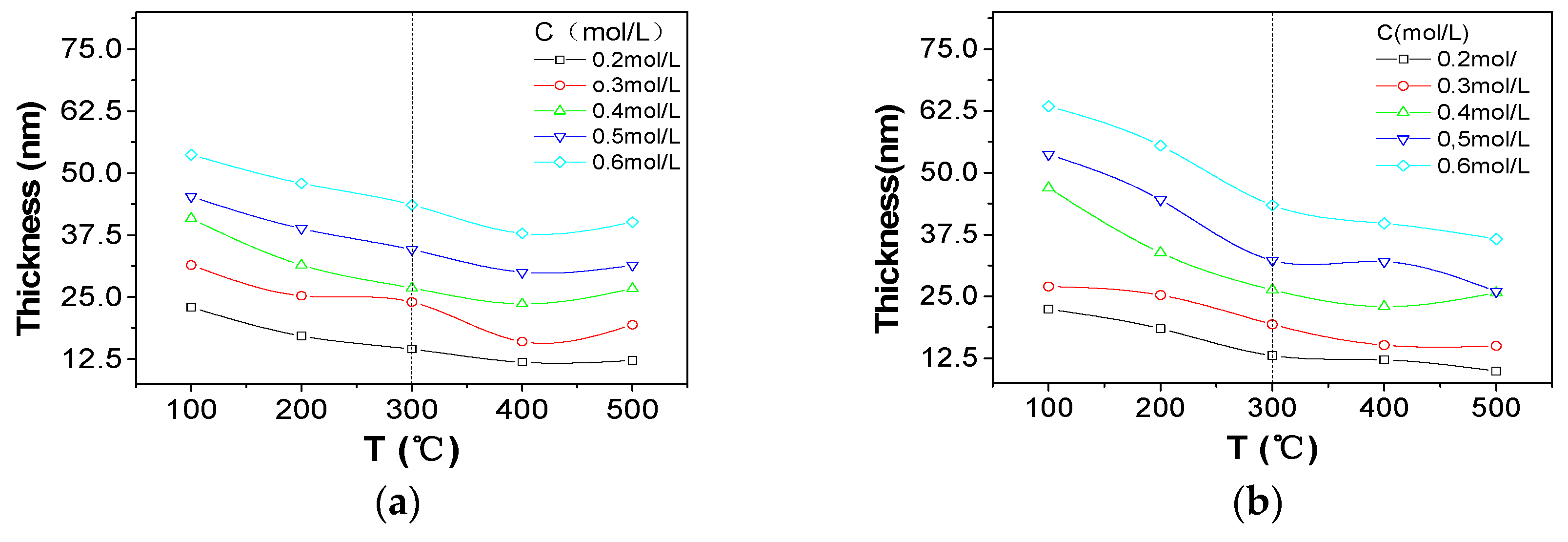
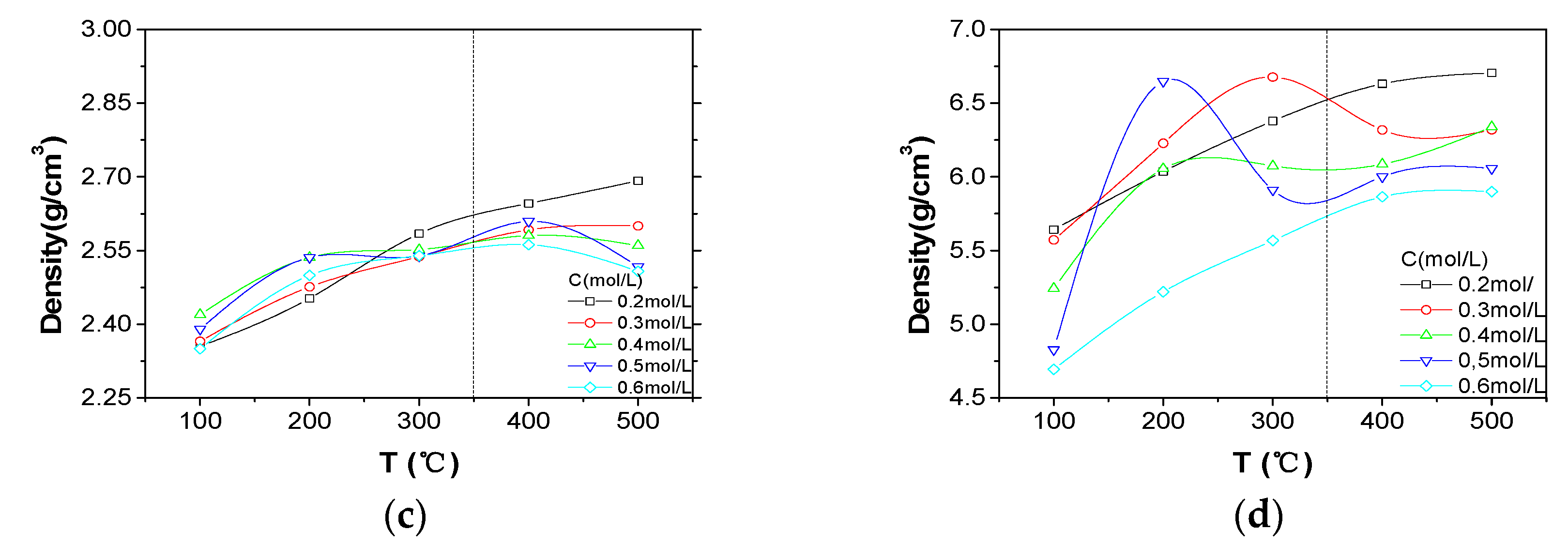
To avoid the difference of properties caused by thickness and density, the optimized annealing temperature was explored by Al2O3 and ZrO2 single layers. As shown in Figure 3a,b, the variations of thickness of Al2O3 and ZrO2 single layers tended to be stable when the annealing temperature was above 300 °C. Similarly, the density fluctuation of ZrO2 and Al2O3 was also suppressed significantly when the temperature was higher than 350 °C, as shown in Figure 3c,d. The results showed that thickness and density were relatively stable when the annealing temperature was over 350 °C. Therefore, 400 °C (between 350 °C and 500 °C) was selected as the annealing temperature.
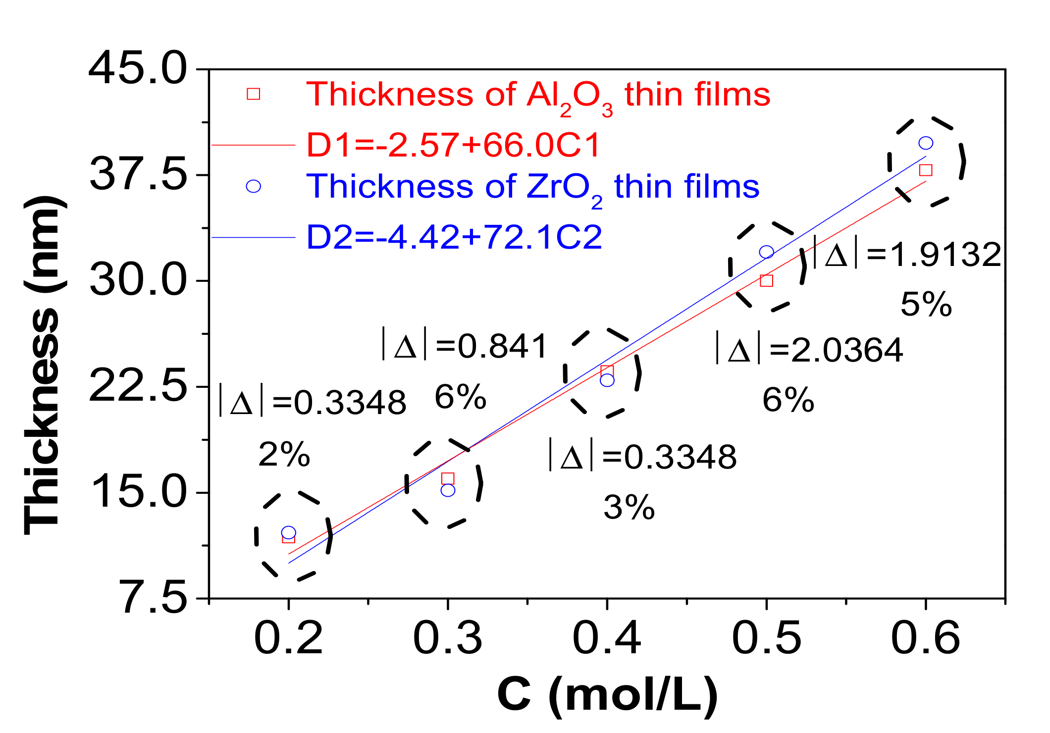
Meanwhile, the percentage marked in Figure 4 showed little difference between the thickness of Al2O3 and ZrO2 single layers, which were coated by precursors with the same concentration. The result was analyzed by mathematical statistics theory, as shown by the linear regression equations in Figure 4. With the concentration increased by 0.1 mol/L, the thicknesses of Al2O3 and ZrO2 were increased by 6.6 nm and 7.21 nm respectively. The result was tested by t-test ( α = 0.05). It was demonstrated that the result was reasonable since the test statistics of Al2O3 ( t Al 2 O 3 = 17.0264) and ZrO2 ( t ZrO 2 = 11.3591) were higher than the critical value ( t 1 α 2 ( n 2 ) = 3.1824 ). Thus, it is believed that the thickness of the layers which were fabricated by precursors with the same concentration were similar.
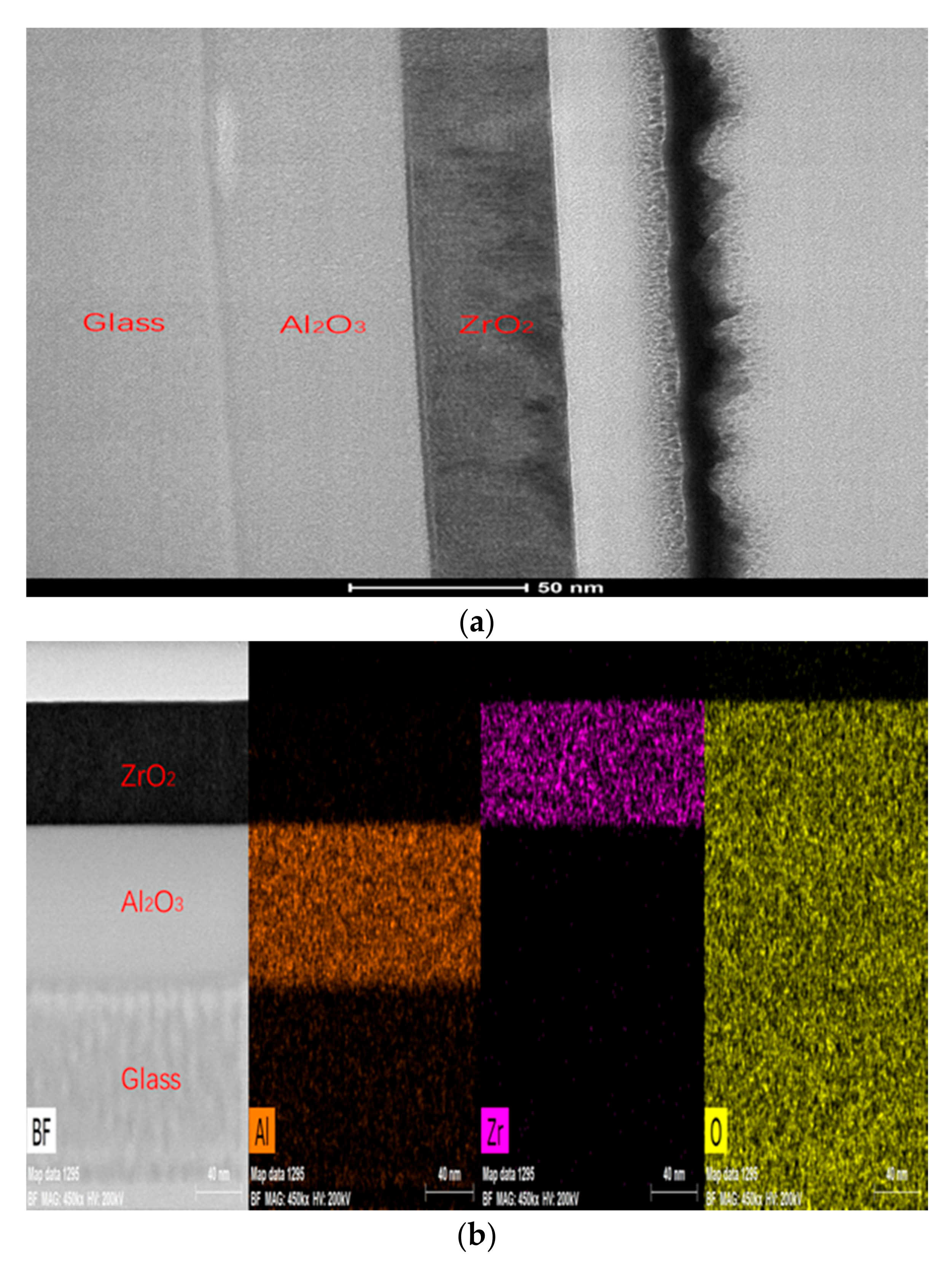
Additionally, it was also demonstrated that the conclusions drawn above were suitable for nanolaminates. First of all, the TEM result showed smooth interfaces of nanolaminates, as shown in Figure 5a. That benefits to the coating of next layer. As meanwhile, the layers were dense and had good contact with each other, which was helpful to avoid defects, such as holes. Secondly, the cross-sectional EDS image of nanolaminates showed that there was no diffusion between Al2O3 and ZrO2, as shown in Figure 5b. Thus, the influence of solution permeation caused by the next coating was avoided, which guaranteed the relative independence of thickness and density. Lastly, as the three samples showed in Figure 6b, the thickness of layers in nanolaminates fabricated by the same precursor were uniform. The ratio of thickness was approximate to the ratio of precursor concentration, and the total thicknesses were all around 70 nm. As the results above show, it was verified that 400 °C was the optimized annealing temperature to fabricate nanolaminates.

3.2. Performance of Nanolaminates

3.2.1. Optical Properties

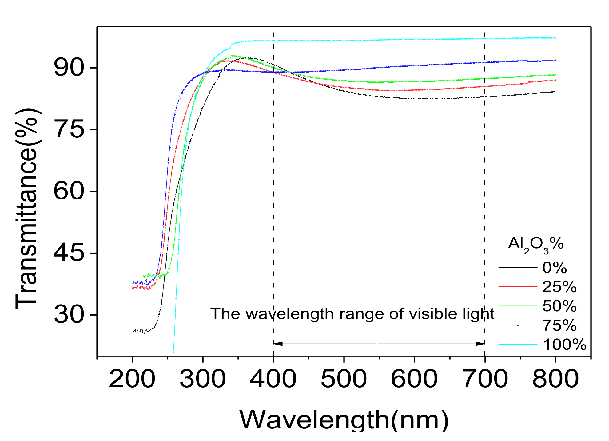
Transmittance of nanolaminates with different contents of Al2O3 (as Table 1) were measured, as shown in Figure 7. The transmittance of nanolaminates fabricated by pure ZrO2 was around 82%, within the range of visible light. With the increase of Al2O3 content, the transmittance was obviously improved and it reached the highest value when the dielectric was fabricated with pure Al2O3.
The optical energy gap of nanolaminates was determined by Tauc formula:
α hv   =   A ( hv E g ) 1 2
where A is a constant, hv and Eg are symbols of photon energy and optical energy gap, and α is the optical absorption coefficient [21]. As shown in Table 2, it was found that the optical energy gap of nanolaminates changed from 4.232 eV to 4.89 eV, exactly between the value of ZrO2 and Al2O3 dielectrics. With the content of Al2O3 increased by 25%, the optical energy gap of nanolaminates were increased around 0.2 eV at the beginning. When the content of Al2O3 was higher than 75%, it was close to the value of the dielectric made with pure Al2O3.

3.2.2. Electrical Properties

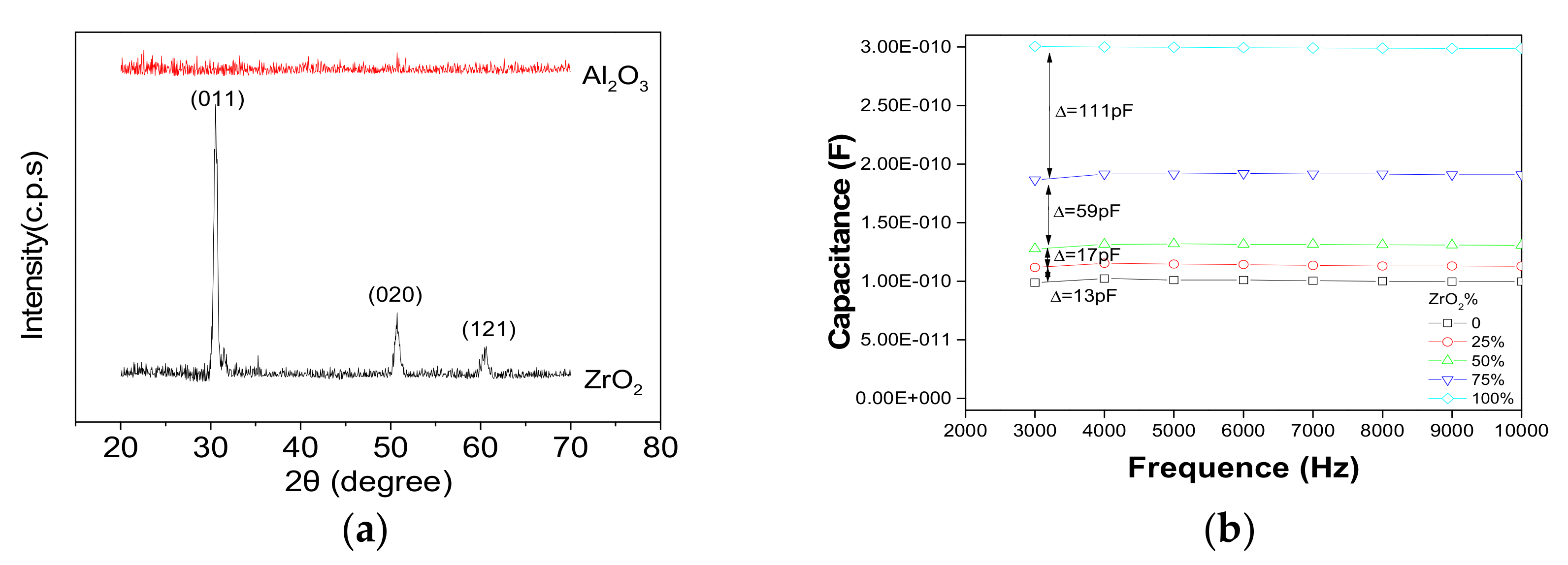
As shown in Table 3, the dielectric strength of ZrO2 was just 0.11 MV/cm. The result measured by XRD showed that the ZrO2 has already crystallized and the corresponding crystallization peaks were shown in Figure 8a [22]. That was the main reason why ZrO2 was easier to break down. The Al2O3 was still amorphous while it was poor at capacitance density compared with ZrO2. Therefore, the nanolaminate structure was applied to combine the advantages of Al2O3 and ZrO2. The results showed that dielectric strength was improved significantly with the increase of Al2O3 content. The increment was up to 0.83 MV/cm when the content of Al2O3 increased from 0% to 25%. Though the variation became smaller when the content of Al2O3 was higher than 50%, it can also be improved on a small scale, as shown in Table 3. Similarly, the capacitance of nanolaminates grew very slowly at the beginning. However, there was a sudden growth when the content of ZrO2 was higher than 50%, as shown in Figure 8b. The capacitance density in Table 3 was the value of capacitance divided by electrode area. Referring to the Formula (2), the relative permittivity was proportional to the capacitance. Therefore, the regular of relative permittivity changed with the content of ZrO2 was similar to the capacitance, as shown in Table 3.
The results shown in Table 2 and Table 3 found that the change of the properties was smaller when the content of Al2O3 was higher than 50%. With the content of Al2O3 changed from 50% to 100%, the variation of the dielectric strength, capacitance density and relative permittivity was only 0.6 MV/cm, 23.88 nF/cm2 and 1.76, respectively. It presented an excellent stability of the dielectric performance. However, the variation of these properties was up to 2.12 MV/cm, 135.35 nF/cm2, and 11.64 when the content of Al2O3 was less than 50%. Thus, there was also a wide scale to adjust the properties of nanolaminates.

3.2.3. The Influence of the Number of Bilayers

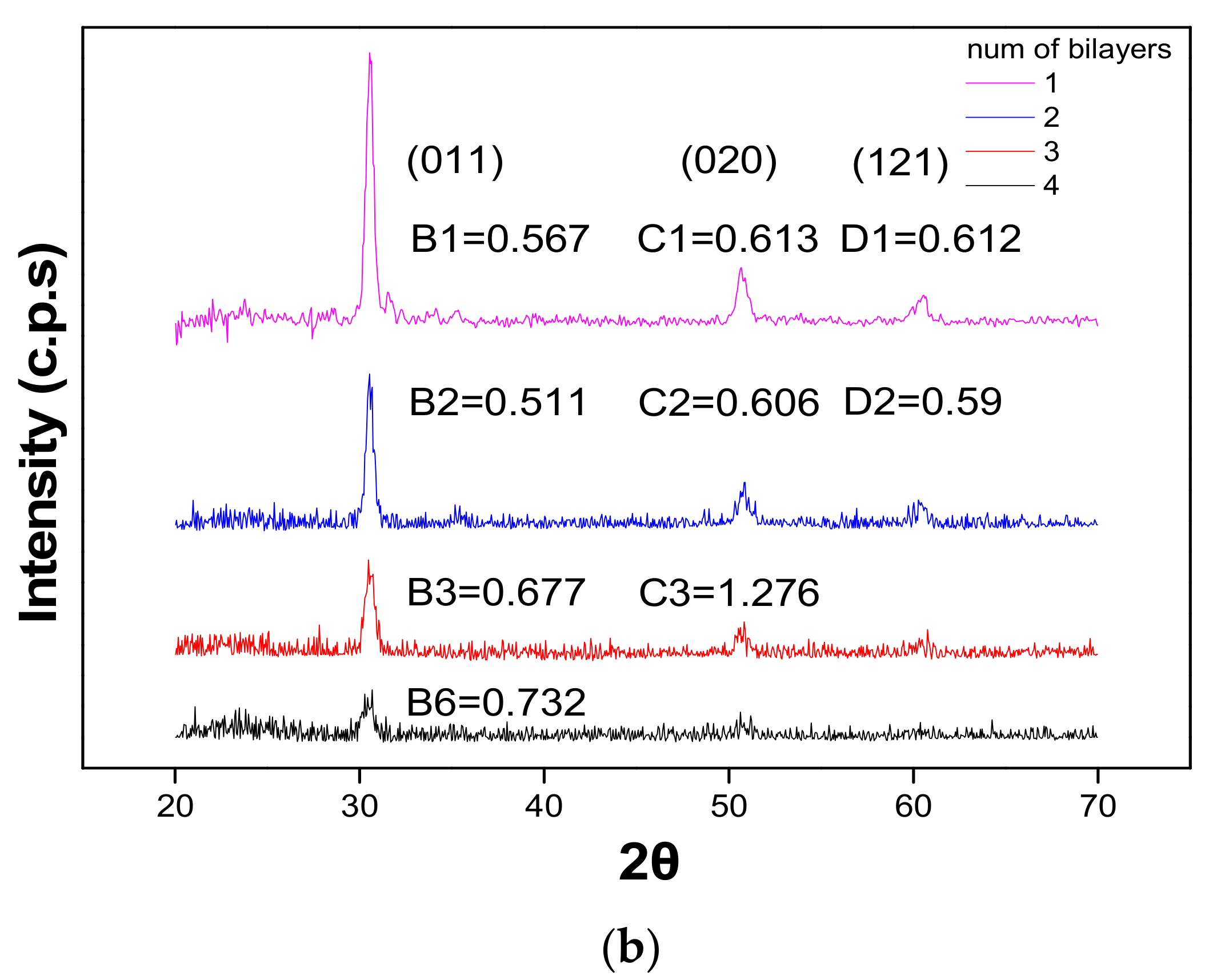
Finally, the influence of the number of bilayers in nanolaminates is discussed. As shown in Table 4, the content of Al2O3 was set to 50% and the number of bilayers was designed as 1, 2, 3, and 6, respectively. The measurement drawn above were carried out. The results showed that the number of bilayers in nanolaminates has little impact on transmittance, optical energy gap, capacitance density, and relative permittivity, as shown in Table 5.
However, the dielectric strength of nanolaminates was influenced significantly by the number of bilayers, as shown in Table 6. The data was analyzed by linear regression and it was found that the dielectric strength was increased by around 0.39 MV/cm with the increase of one bilayer. The general changing tendency of dielectric strength can be concluded as the equation:
V ds   =   0.86   +   0.39 n
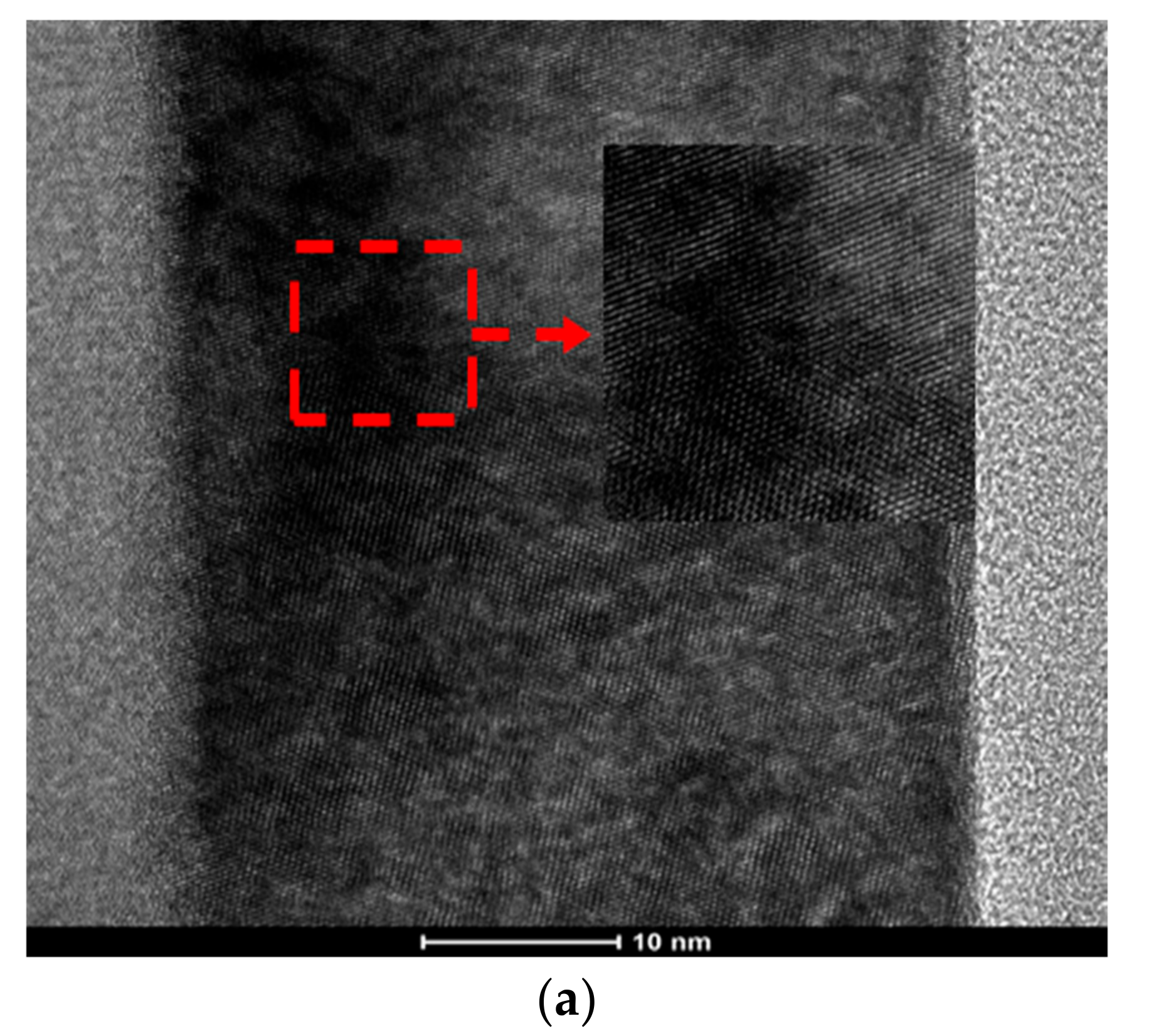
where n is the number of bilayers. When the bilayer number was up to six, it was comparable to the dielectric fabricated with pure Al2O3. The main reason was that the crystallite grain boundaries in ZrO2 were interrupted by amorphous Al2O3. Crystallite grain boundaries which contain leakage current spots were located at ZrO2 thin films [23,24], as shown in Figure 9a. These boundaries provided paths for leakage current and led to the easy breakdown of the dielectric. However, these paths were interrupted by amorphous Al2O3 in the nanolaminate structure. It was helpful to improve the dielectric strength. Another reason might be that the variation of crystallite size was not distinct with the change of bilayers. With the increase in the number of bilayers, the thickness per layer was decreased, which might cause a decrease in the average crystallite size. The FWHM corresponding to different peaks were measured by Data Viewer, as shown in Figure 9b, and the average crystallite size was calculated by Scherrer' equation (the average result of the peaks which can be detected by Data Viewer), as shown in Table 6. When the number of bilayers was up to six, the average crystallite size did not present an obvious change. It was helpful to resist the leakage current, which was beneficial to Vds [25,26].

4. Conclusions

In summary, 400 °C was demonstrated to be the optimized annealing temperature for nanolaminates fabricated by spin-coating. By changing the content of components and the number of bilayers, the properties control of the dielectric was achieved. Increasing the content of Al2O3 in nanolaminates was helpful to improve the transmittance, optical energy gap and dielectric strength of dielectric, while the capacitance density and relative permittivity were improved by adjusting the content of ZrO2. It was also found that the electrical properties of the dielectric were relatively stable when the content of Al2O3 was higher than 50% in nanolaminates, while variation of electrical properties became larger when the content of Al2O3 was less than 50%. Additionally, increasing the number of bilayers in nanolaminates can improve the dielectric strength because the grain boundaries of ZrO2 were interrupted by amorphous Al2O3.

Acknowledgments

This work was supported by the National Key R and D Program of China (No. 2016YFB0401504), NSFC (51771074, U1601651), the National Key Basic Research and Development Program of China (973 program, grant No. 2015CB655004) founded by MOST, the Guangdong Natural Science Foundation (2016A030313459, 2017A030310028), the Science and Technology Project of Guangdong Province (2014B090915004, 2016B090907001), the Project for Guangdong Province Universities and Colleges Pearl River Scholar Funded Scheme (2016), and the Open Funds of Key Laboratory of Advanced Display and System Applications, Shanghai University, China (P201605).

Author Contributions

The main manuscript text was written by Junbiao Peng and Jinglin Wei. Hong Tao, Yanqiong Zheng, and Xubing Lu provided the equipment for characteristics testing of the samples. References were searched by Wei Cai, Zhennan Zhu and Kuankuan Lu. Honglong Ning and Rihui Yao provided advice about the content and the structure of this work.

Conflicts of Interest

The authors declare no conflicts of interest.

References

  1. Fakhri, M.; Theisen, M. Top-gate zinc tin oxide thin-film transistors with high bias and environmental stress stability. Appl. Phys. Lett. 2014, 104, 251603. [Google Scholar] [CrossRef]
  2. Waggoner, T.; Triska, J. Zirconium oxide-aluminum oxide nanolaminate gate dielectrics for amorphous oxide semiconductor thin-film transistors. Am. Vac. Soc. 2011, 29, 04D115. [Google Scholar] [CrossRef]
  3. López, J.; Sotelo, A. Influence of the bilayer thickness on the optical properties of Al2O3-Y2O3 dielectric nanolaminate films grown by thermal atomic layer deposition. Mater. Res. Bull. 2017, 87, 14–19. [Google Scholar] [CrossRef]
  4. Nehm, F.; Dollinger, F. Atomic layer deposited TiOx/AlOx nanolaminates as moisture barriers for organic devices. Org. Electron. 2016, 38, 84–88. [Google Scholar] [CrossRef]
  5. Krylov, I.; Pokroy, B. A comparison between HfO2/Al2O3 nano-laminates and ternary HfxAlyO compound as the dielectric material in InGaAs based metal-oxide-semiconductor (MOS) capacitors. J. Appl. Phys. 2016, 120, 124505. [Google Scholar] [CrossRef]
  6. Rowlette, P.C.; Wolden, C.A. Pulsed plasma-enhanced chemical vapor deposition of Al2O3-TiO2 nanolaminates. Thin Solid Films 2010, 518, 3337–3341. [Google Scholar] [CrossRef]
  7. Song, X.; Christos, G. Cyclic Chemical-Vapor-Deposited TiO2/Al2O3 Film Using Trimethyl Aluminum, Tetrakis(diethylamino)titanium. Electrochem. Soc. 2007, 154, G177–G182. [Google Scholar] [CrossRef]
  8. Son, B.; Je, S.Y. High-performance In-Zn-O thin-film transistors with a soluble processed ZrO2 gate insulator. Phys. Status Solidi (RRL)-Rapid Res. Lett. 2013, 7, 485–488. [Google Scholar] [CrossRef]
  9. Stephen, T; Jeremy, T. Solution-Processed Aluminum Oxide Phosphate Thin-Film Dielectrics. Chem. Mater. 2007, 19, 4023–4029. [Google Scholar] [CrossRef]
  10. Yoo, Y.B.; Park, J.H. Solution-processed high-k HfO2 gate dielectric processed under softening temperature of polymer substrates. J. Mater. Chem. C 2013, 1, 1651. [Google Scholar] [CrossRef]
  11. Chang, S.; Doong, R. ZrO2 thin films with controllable morphology and thickness by spin-coated sol-gel method. Thin Solid Films 2005, 489, 17–22. [Google Scholar] [CrossRef]
  12. Song, K.; Yang, W. A solution-processed yttrium oxide gate insulator for high-performance all-solution-processed fully transparent thin film transistors. J. Mater. Chem. 2012, 22, 21265–21271. [Google Scholar] [CrossRef]
  13. Wang, C.; Hsieh, C. Flexible Organic Thin-Film Transistors with Silk Fibroin as the Gate Dielectric. Adv. Mater. 2011, 23, 1630–1634. [Google Scholar] [CrossRef] [PubMed]
  14. Tong, J.; Wan, Y. Solution-processed molybdenum oxide for hole-selective contacts on crystalline silicon solar cells. Appl. Surf. Sci. 2017, 423, 139–146. [Google Scholar] [CrossRef]
  15. Lisco, F.; Shaw, A. Atmospheric-pressure plasma surface activation for solution processed photovoltaic devices. Sol. Energy 2017, 146, 287–297. [Google Scholar] [CrossRef]
  16. Hamid, S.; Saeed, P. The Relationship between Religious Coping and Self-Care Behaviors in Iranian Medical Students. J. Relig. Health 2017, 56, 2109–2117. [Google Scholar]
  17. Yao, J.; Wu, L.; Meng, X.; Yang, H.; Ni, S.; Wang, Q.; Zhou, J.; Zhang, Q.; Su, K.; Shao, L.; et al. Profiling, clinicopathological correlation and functional validation of specific long noncoding RNAs for hepatocellular carcinoma. Mol. Cancer 2017, 16, 164. [Google Scholar] [CrossRef] [PubMed]
  18. Chand, P.; Vaish, S. Structural, optical and dielectric properties of transition metal (MFe2O4; M = Co, Ni and Zn) nanoferrites. Phys. B Condens. Matter 2017, 524, 53–63. [Google Scholar] [CrossRef]
  19. Moosavi, S.; Zakaria, S. Hydrothermal synthesis, magnetic properties and characterization of CoFe2O4 nanocrystals. Ceram. Int. 2017, 43, 7889–7894. [Google Scholar] [CrossRef]
  20. Shanker, J.; Prasad, B.V. Electrical properties of NdCr1-xFexO3 perovskite ceramic nanoparticles—An impedance spectroscopy studies. Mater. Res. Bull. 2017, 94, 385–398. [Google Scholar] [CrossRef]
  21. Farajimotlagh, M.; Poursalehi, R. Synthesis mechanisms, optical and structural properties of η-Al2O3 based nanoparticles prepared by DC arc discharge in environmentally friendly liquids. Ceram. Int. 2017, 43, 7717–7723. [Google Scholar] [CrossRef]
  22. Cai, W.; Zhu, Z. A Simple Method for High-Performance, Solution-Processed, Amorphous ZrO2 Gate Insulator TFT with a High Concentration Precursor. Materials 2017, 10, 972. [Google Scholar] [CrossRef] [PubMed]
  23. Vasil, Y.; Mathias, R. Tunneling atomic-force microscopy as a highly sensitive mapping tool for the characterization of film morphology in thin high-k dielectrics. Appl. Phys. Lett. 2008, 92, 252910. [Google Scholar]
  24. Dominik, M.; Matthias, G. Mesoscopic analysis of leakage current suppression in ZrO2/Al2O3/ZrO2 nanolaminates. J. Appl. Phys. 2013, 113, 194103. [Google Scholar] [CrossRef]
  25. Han, R.; Jin, J. Effect of crystal structure on polarization reversal and energy storage of ferroelectric poly (vinylidene fluoride-co-chlorotrifluoroethylene) thin films. Polymer 2012, 53, 1277–1281. [Google Scholar] [CrossRef]
  26. Wang, Y.; Zhang, J. Strength Weakening by Nanocrystals in Ceramic Materials. Nano Lett. 2007, 7, 3196–3199. [Google Scholar] [CrossRef] [PubMed]
Figure 1. Plot of nanolaminates and bilayers on glass.
Nanomaterials 07 00419 g001
Figure 2. Plot of the MIM device.
Nanomaterials 07 00419 g002
Figure 3. Thickness and density of Al2O3 and ZrO2 single layers tested by XRR: (a) the plot of thickness versus temperature (T) of Al2O3 single layers; (b) the plot of thickness versus temperature (T) of ZrO2 single layers; (c) the plot of density versus temperature (T) of Al2O3 single layers; (d) the plot of density versus temperature of ZrO2 single layers. C presented in the legend is the concentration of the solution.
Nanomaterials 07 00419 g003aNanomaterials 07 00419 g003b
Figure 4. Plot of thickness versus concentration (C) of Al2O3 and ZrO2 single layers (annealed at 400 °C). |Δ| is the absolute difference value of thickness between Al2O3 and ZrO2. Percentage under the |Δ| is the relative error calculated by the ratio of |Δ| and thickness, the thickness is picked out from the smaller of Al2O3 and ZrO2. D1 and D2 are equations of linear regression of the thickness and precursor concentration.
Nanomaterials 07 00419 g004
Figure 5. (a) The cross-sectional HR-TEM image of nanolaminates which contains one bilayer (the main parameters are shown in Table 4). (b) The cross-sectional EDS image of nanolaminates.
Nanomaterials 07 00419 g005
Figure 6. (a) The XRR measurements of three nanolaminate samples and (b) their corresponding histogram of thickness of different layers of nanolaminates. The combination of precursors is shown in the legend. A and Z present Al(NO3)3 and ZrOCl2, respectively, and in the figure before A and Z represent the concentration of precursors.
Nanomaterials 07 00419 g006
Figure 7. Plot of transmittance versus wavelength.
Nanomaterials 07 00419 g007
Figure 8. (a) X-ray diffraction plot of dielectrics fabricated with pure Al2O3 and ZrO2 (annealing at 400 °C in the air); and (b) capacitance versus the frequency plot of nanolaminates with different contents of ZrO2. Δ represent the difference value of capacitance.
Nanomaterials 07 00419 g008
Figure 9. (a) HR-TEM image of ZrO2; (b) X-ray diffraction of nanolaminates fabricated with different numbers of bilayers (annealing at 400 °C in the air). B, C and D are the FWHM corresponding to the (011), (020), and (121) peaks, respectively.
Nanomaterials 07 00419 g009aNanomaterials 07 00419 g009b
Table 1. Nanolaminates with different contents of Al2O3: n1 is the coating time; n2 is the number of bilayers in the nanolaminates; and C1 and C2 are the concentration of Al(NO3)3 and ZrOCl2.
Al2O3%n1n2C1 (mol/L)C2 (mol/L)
020-0.6
25630.10.3
50630.20.2
75630.30.1
100200.6-
Table 2. The optical energy gap (Eg) of nanolaminates with different contents of Al2O3.
Al2O3%0%25%50%75%100%
Eg (eV)4.2324.504.664.854.89
Table 3. Dielectric strength (Vds), capacitance density (Cd), and relative permittivity ( ε r ) of nanolaminates with different contents of Al2O3.
Al2O3%0%25%50%75%100%
Vds (MV/cm)0.110.942.232.462.83
Cd (nF/cm2)238.85155.25103.5091.5679.62
ε r 20.313.28.667.666.9
Table 4. Nanolaminates with different numbers of bilayers. n3 is the coating time; n4 is the number of bilayers in nanolaminates; and C3 and C4 are the concentration of Al(NO3)3 and ZrOCl2.
Al2O3%n3n4C3(mol/L)C4(mol/L)
50210.60.6
50420.30.3
50630.20.2
501260.10.1
Table 5. Transmittance (T), optical energy gap (Eg), capacitance density (Cd), and relative permittivity ( ε r ) of nanolaminates with different numbers of bilayers.
T (%)Eg (eV)Cd (nF/cm2) ε r
87 ± 1.44.65 ± 0.05120 ± 78.7 ± 0.5
Table 6. Dielectric strength (Vds) and average crystallite size (D) of nanolaminates with different numbers of bilayers.
Number 1236
Vds (MV/cm)1.091.712.233.14
D(nm)14.4715.249.4211.13