Article

Enhancing the Performance of Si/Ga2O3 Heterojunction Solar-Blind Photodetectors for Underwater Applications

1
College of Chemistry, Fuzhou University, Fuzhou 350108, China
2
State Key Laboratory of Functional Crystals and Devices Fujian Institute of Research on the Structure of Matter, Chinese Academy of Sciences, Fuzhou 350002, China
3
Fujian College, University of Chinese Academy of Sciences, Fuzhou 350002, China
*
Author to whom correspondence should be addressed.
Nanomaterials 2025, 15(14), 1137; https://doi.org/10.3390/nano15141137
Submission received: 17 June 2025 / Revised: 16 July 2025 / Accepted: 19 July 2025 / Published: 21 July 2025

Abstract

Epitaxial growth of β-Ga2O3 nanowires on silicon substrates was realized by the low-pressure chemical vapor deposition (LPCVD) method. The as-grown Si/Ga2O3 heterojunctions were employed in the Underwater DUV detection. It is found that the carrier type as well as the carrier concentration of the silicon substrate significantly affect the performance of the Si/Ga2O3 heterojunction. The p-Si/β-Ga2O3 (2.68 × 1015 cm−3) devices exhibit a responsivity of up to 205.1 mA/W, which is twice the performance of the devices on the n-type substrate (responsivity of 93.69 mA/W). Moreover, the devices’ performance is enhanced with the increase in the carrier concentration of the p-type silicon substrates; the corresponding device on the high carrier concentration substrate (6.48 × 1017 cm−3) achieves a superior responsivity of 845.3 mA/W. The performance enhancement is mainly attributed to the built-in electric field at the p-Si/n-Ga2O3 heterojunction and the reduction in the Schottky barrier under high carrier concentration. These findings would provide a strategy for optimizing carrier transport and interface engineering in solar-blind UV photodetectors, advancing the practical use of high-performance solar-blind photodetectors for underwater application.

1. Introduction

Solar-blind photodetectors (SBPDs) exploit their insensitivity to sunlight within the 200–280 nm spectral band, enabling critical applications in space security communications, ozone layer monitoring, missile early warning, and underwater target identification [1,2,3,4]. SBPDs are uniquely indispensable for underwater detection due to their inherent immunity to solar background noise, selective sensitivity to trace DUV signatures, and compatibility with the deep ultraviolet transmission window in aquatic environments. As a result, SBPDs are increasingly recognized as a key component in the development of next-generation marine exploration systems, autonomous underwater vehicles (AUVs), and underwater photodetectors [5,6,7,8].
In addition to spectral selectivity, the materials used in the underwater detection must also exhibit strong chemical stability and corrosion resistance in aqueous solutions and typically ion-rich environments. Due to their resistance to hydrolysis and surface oxidation, materials with strong chemical inertia (such as diamond, AlGaN alloys, and β-Ga2O3) are preferred [9]. Distinct from solid-state counterparts, underwater photodetectors necessitate fully autonomous operation without external electrodes or power inputs, mandating robust self-powered characteristics in device design [10,11,12].
Gallium oxide (Ga2O3) is a novel ultra-wideband semiconductor material characterized by high absorption coefficients and excellent stability. Its direct bandgap is approximately 4.9 eV, located in the solar-blind region. Compared with other candidate materials such as diamond and AlGaN, β-Ga2O3 combines an exceptional chemical inertness with a uniquely wide bandgap (4.8 eV), yielding intrinsically solar-blind deep-UV selectivity without the need for complex heterostructuring or expensive substrates. Additionally, β-Ga2O3 exhibits high transparency in the visible light spectrum and low growth costs, making it one of the most suitable materials for manufacturing SBUV detectors [13,14]. Chen et al. recently reported a photodiode (PD) based on an α-Ga2O3 nanorod array (NRA), with a response/recovery time (τrd = 0.43/0.17 s) and responsivity of 1.44 mA/W [15]. Huang et al. further developed α-Ga2O3 NRAs PDs, which increased the responsivity to 11.34 mA/W, with τrd values of 1.51/0.18 s [16]. Feng et al. synthesized an array of β-Ga2O3 nanorods coated with an amorphous Ga2O3 layer on a silicon substrate, with a response rate of 48.4 mA/W and a response/recovery time of 0.12/0.16 s [17]. Existing research has made significant progress in material and device optimization [18,19]. However, compared to traditional SBPDs, the performance of underwater devices remains relatively limited, largely due to the lack of systematic investigation into the impact of substrate material properties on device performance.
Here, we present the growth of β-Ga2O3 nanowires (NARs) with good crystallinity on silicon substrates with different doping types and doping concentrations by a simple CVD technique. Subsequently, DUV PDs based on β-Ga2O3 NRAs were prepared, and the obtained PDs exhibited self-powered solar-blind DUV detection with a high responsivity of 845.3 mA/W at 254 nm and 0.6 mW/cm2 light intensity. Then, the reliability of the prepared β-Ga2O3 PDs is explored. These results indicate that β-Ga2O3 nanostructures are promising candidates for low-cost, self-powered, high-sensitivity solar-blind DUV PD applications in next-generation sustainable integrated optoelectronic systems.

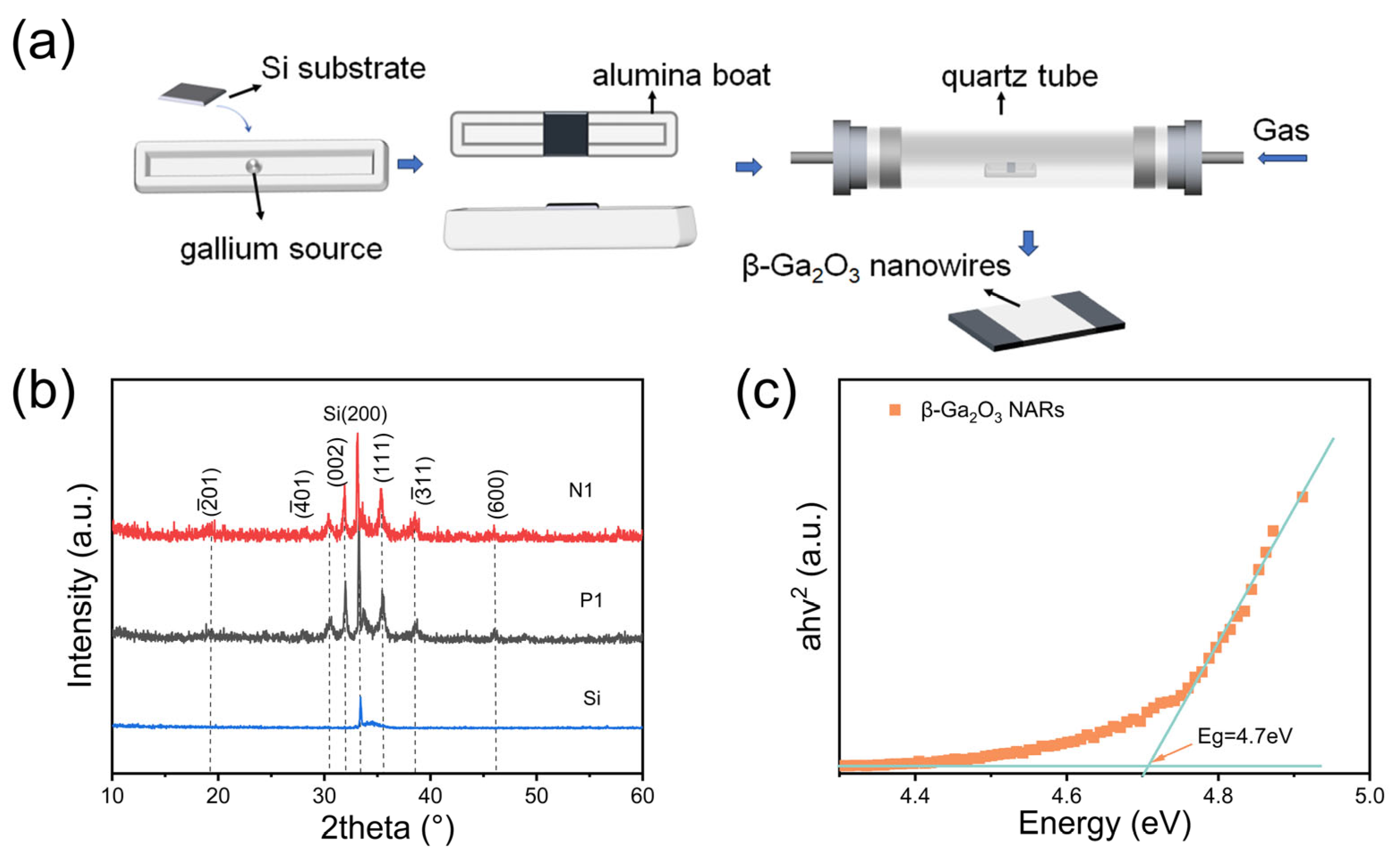
2. Materials and Methods

β-Ga2O3 NARs were epitaxially grown on silicon substrates by the LPCVD technique. High-purity gallium (UMC, Hsinchu, Taiwan, 99.99999%) and oxygen (O2, 99.9%) were used as raw material precursors, and argon (Ar, 99.999%) was used as the carrier gas for the experiments. Figure 1a demonstrates a typical preparation process for β-Ga2O3 PDs. The specific process parameters were as follows: the gallium source mass was 10.0 mg, the reaction chamber pressure was set at 15 Torr, and the oxygen flow rate was precisely controlled at 20.0 sccm.
Substrate pre-treatment stage: One-sided polished (100) crystal-oriented silicon substrate (size 10 mm × 10 mm) was selected and immersed in 5% HF dilution for 5 min to remove the surface oxide layer. After immersion, the silicon substrate was rinsed with deionized water and ultrasonicated with acetone, deionized water, and ethanol for 10 min. The gold film was deposited via magnetron sputtering at room temperature for 10 s, yielding a uniform thickness of 5.0 ± 0.5 nm. The treated substrate was placed in a ceramic boat (size 8 cm × 1.2 cm) directly above the gallium source.
Growth process control: The tube furnace chamber was first pumped to a high vacuum (<10−2 Torr), followed by the introduction of high-purity argon at a constant flow rate (100 sccm) as a protective atmosphere. The temperature was rapidly increased at a rate of 20 °C/min to 710 °C, then slowly increased to 752 °C, and a 30 min gas phase reaction was carried out while introducing Ar (100 sccm) and O2 (20.0 sccm). At the end of growth, the atmosphere was switched to pure argon atmosphere (100 sccm) and naturally cooled to room temperature.
Substrate parameter design: n-type and p-type doped silicon substrates are selected for the experiment. Specifically, they are divided into four groups (P1 (p-type, 2.68 × 1015 cm−3), P2 (p-type, 3.19 × 1016 cm−3), P3 (p-type, 6.48 × 1017 cm−3), and N1 (n-type, 8.95 × 1014 cm−3)) to systematically study the effects of the substrate carrier type and carrier concentration on the performance of the heterojunction.
The synthesized samples were characterized by X-ray diffraction (XRD) to determine crystal structures and phase purity, and scanning electron microscopy (SEM) to analyze surface morphology. The XRD patterns were collected using a high-resolution X-ray diffractometer at Rigaku Smart Laboratory, Tokyo, Japan. The samples were scanned in the range of 10–60° using a scanning speed of 2°/min. The surface elemental compositions of Ga2O3 nanowires were characterized and performed with an X-ray photoelectron spectrometer (XPS) model ESCALAB Xi+ from Thermo Fisher, Waltham, MA, USA. Al Kα rays (energy 1486.68 eV) were used as the excitation source and the X-ray spot diameter was 650 μm. The elements scanned were C, Si, Ga, and O. Binding energies were scanned in the range 0–1400 eV in 0.1 eV steps. The data were then analyzed using the Avantage program and all XPS binding energies were calibrated to the C 1s peak at 284.8 eV before peak fitting, and the appropriate charge correction was applied to obtain accurate binding energy values. SEM images were taken at 15.0 kV using a HITACHIUHR SU8010, Tokyo, Japan. The UV transmission spectra of β-Ga2O3 NARs were studied using a UV–visible spectrophotometer (UV-2550) in the wavelength range of 200–600 nm. It was tested in a three-electrode quartz cell with high DUV transmittance by an electrochemical workstation (CHI440C, Shanghai Chenhua Co., Ltd., Shanghai, China). A silicon substrate on which β-Ga2O3 NARs were grown was used as the working electrode. A platinum sheet (1 × 1 cm2) and an Ag/AgCl electrode (RHE) were chosen as the counter electrode and reference electrode, respectively. The test environment was 0.5 M Na2SO4 aqueous solution (weakly alkaline), and the UVC light source was provided by low-pressure lamps with wavelengths of 254 nm and 365 nm.

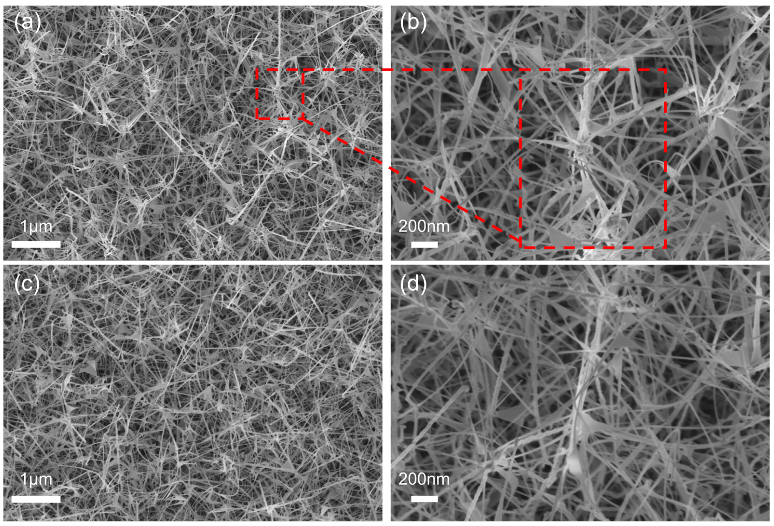
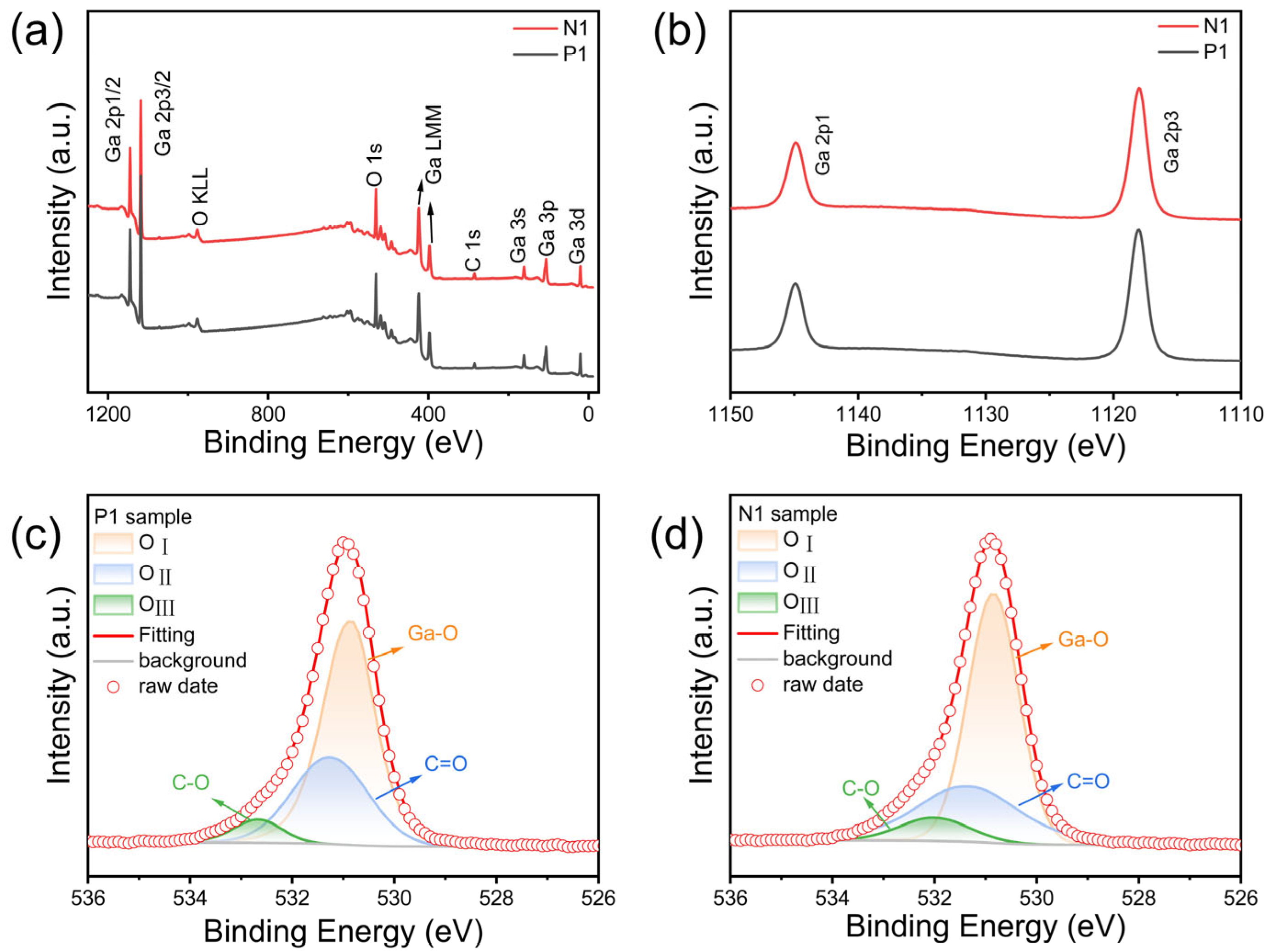
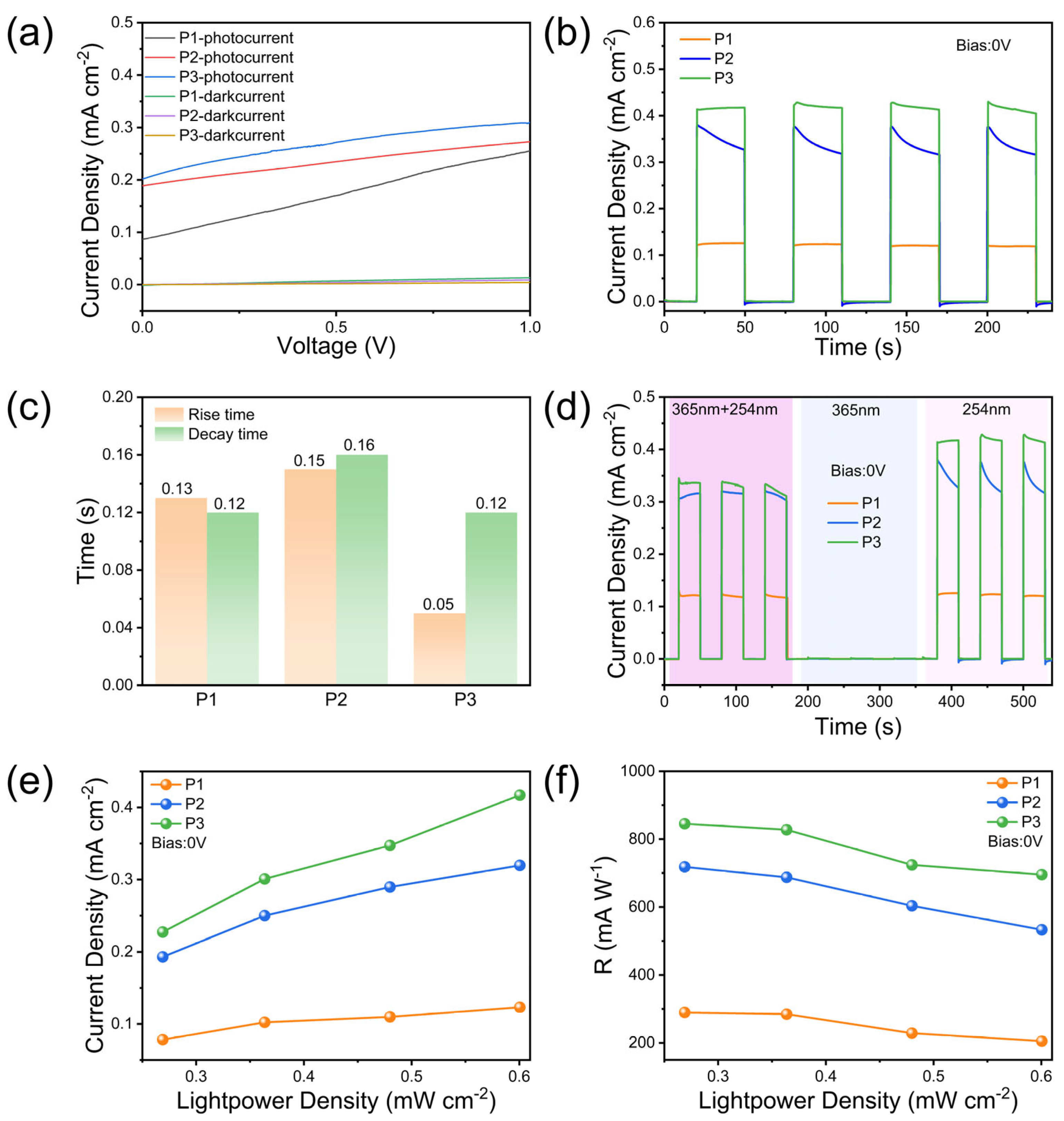
3. Result and Discussion

Figure 1b shows the XRD patterns of β-Ga2O3 NARs grown on the n-type silicon substrate (N1) and p-type silicon substrate (P1), respectively, in which there are multiple diffraction peaks of β-Ga2O3, among which, the diffraction peaks located at 18.9°, 30.5°, 31.7°, 35.2°, 38.4°, and 45.8° correspond to the β-Ga2O3 (201), (401), (002), (111), (311), and (600) diffraction surfaces, and these peaks confirm the formation of β-Ga2O3 (PDF#76-0573). The peak at 33.4° is confirmed to be the diffraction peak of the Si substrate (200) (PDF#27-1402). As can be seen from the figure, there is no significant difference in the peak positions and peak intensities between the two samples, and the difference in the half peak widths (FWHM) is less than 5%, which confirms that the different doping types of the substrate have a negligible effect on the crystal growth kinetics of β-Ga2O3. The UV–Vis transmission spectrum of β-Ga2O3 NARs is shown in Figure 1c, which was fitted to the direct bandgap semiconductor based on Tauc’s formula: ( α h ϑ ) 2 = A ( h ϑ E g ) , where α is the absorption coefficient, hν is the photon energy, and A is the proportionality constant. By linearly extrapolating the intercept of the ( α h ϑ ) 2 versus the h ϑ curve, the optical bandgap of β-Ga2O3 NARs is determined to be 4.70 ± 0.05 eV.
The surface morphology of β-Ga2O3 NARs was verified by SEM (shown in Figure 2), and it can be seen that the samples are in the state of nanowires and have a homogeneous diameter of about 20 nm, with lengths ranging from a few micrometers to a dozen micrometers, The nanowires are cross-connected in a random orientation and form a cross-linked structure at the contact points. The red box is the cross-linked part. Cross-linking facilitates carrier transport by establishing an extensive conductive network, thereby improving electrical performance. It is noteworthy that the substrate carrier type has a negligible effect on the kinetic process of the gas–liquid–solid (VLS) growth mechanism. This stable morphology provides a material basis for large-scale integrated optoelectronic devices.
To understand the surface chemical state and composition of β-Ga2O3, we performed an XPS study on samples N1 and P1, as shown in Figure 3. The XPS was calibrated by measuring the power functions of the samples. The C 1s peak as a reliable binding energy (BE) reference depends on the power function ( S A ) of the samples [20]. The value of S A is related to the following equation: S A = h ϑ + E c u t o f f E F , where E c u t o f f is the fitted value of the cut-off edge, E F is the Fermi energy level, and the β-Ga2O3 power function is calculated to be 4.1 eV [21]. In addition, the position of the C1s peaks was calibrated to be 285.48 eV [22,23] according to the equation E B F = 289.58 S A . It is clear from Figure 3a that the elemental peaks other than the C, Ga, and O peaks were not detected in the XPS measurement spectra, indicating the high purity of the grown β-Ga2O3 nanowires. Figure 3b shows the Ga 2p spectra of the two samples. It is observed that the binding energy peaks of Ga 2p1/2 and Ga 2p3/2 are separated by 27.0 eV, which is consistent with the binding energy of Ga 2p [24,25]. Figure 3c,d shows the division of the O1s core energy level spectra into three components by Gaussian fitting analysis. These components are lattice oxygen (OI), i.e., the oxygen atom bonded to the gallium atom in β-Ga2O3, which represents the oxygen environment of the material proper; O2− (OII) in the oxygen-deficient region; and carbonate and hydroxyl-(OIII), which corresponds to the chemical adsorption on the surface of the film, respectively [26,27]. The density of oxygen vacancies is determined by the intensity ratio of OII/(OI + OII). The calculated intensity ratios of P1 and N1 are 31.03% and 30.07%, respectively.
The similar morphology and XPS spectra observed in both samples indicate good experimental repeatability and reliability. Furthermore, the carrier type of the silicon substrate exerts negligible influence on the film structure and electrochemical properties of the β-Ga2O3 NARs. Similar oxygen vacancy concentrations may result in similar sample performance, given the established correlation between oxygen vacancies and device characteristics [28,29]. However, electrochemical measurements reveal significant performance discrepancies among p-n junction devices. Figure 4a shows a schematic of the experimental test configuration based on the three-electrode system, and all electrochemical characterizations were conducted at constant temperature (25 ± 0.5 °C). Notably, at 254 nm illumination and 0 V bias (Figure 4b), sample P1 exhibits a current density approximately fivefold higher than sample N1. When the bias voltage increases from 0 V to 1 V (−0.6~0.4 V vs. RHE), the photocurrent density of the P1 detector rises sharply to 0.25 mA/cm2—two orders of magnitude above its dark current. This demonstrates that the fabricated PDs operate effectively in self-powered mode (0 V) while maintaining excellent optoelectronic responsivity. Given the pronounced sensitivity of semiconductor/electrolyte photodetectors to external parameters, the impact of applied bias voltage on device performance was systematically investigated. As depicted in Figure 4c, both P1 and N1 detectors exhibit defined on/off switching characteristics across a 0–1 V bias range at 30 s intervals, demonstrating high signal reproducibility. A quantitative relationship between photocurrent enhancement and increasing bias voltage is observed, indicating improved separation efficiency of photogenerated carriers at elevated electric fields. Consequently, systematic modulation of the bias voltage serves as a critical factor for optimizing detection performance [30].
The rise time (τr) and decay time (τd) are defined as the time required for the photocurrent to rise to 90% and fall to 10% of the peak value, respectively [31]. As evidenced in Figure 4d,e, both samples demonstrate rapid response kinetics (τr, τd< 0.2 s at 0 V bias), with the P1 device exhibiting marginally faster response times (τr, τd < 0.15 s) compared to N1. Figure 4f presents the characteristic self-powered switching behavior under varied illumination wavelengths (0 V bias). Notably, both devices exhibit no detectable photoresponse under 365 nm irradiation. Conversely, abrupt photoresponse onset occurs upon 254 nm UV illumination, where the photocurrent rapidly saturates at 0.12 mA/cm2 (P1 sample). Crucially, concurrent 365/254 nm illumination yields identical response characteristics to 254 nm irradiation alone. To quantify this selectivity, we introduce the rejection ratio: R r e j = I 254   n m I 365   n m , where I254 nm and I365 nm are the steady-state photocurrents under 254 nm and 365 nm illumination, respectively, at the same optical power density. The results are shown in Table 1. These results collectively validate pronounced solar-blind UV selectivity in the fabricated devices [16,17]. As a fundamental performance metric for photodetectors, the photocurrent is defined as the incremental current generated by photogenerated carriers. Figure 4g presents the characteristic self-powered switching behavior under varied light intensities (0 V bias) and corresponding photoresponse calculations. This linear dependence further indicates the efficient separation of photoexcited electron–hole pairs with minimal trap-state involvement [32,33]. The photoresponsivity (R) is defined as the ratio of the photocurrent Iph to the incident light power Pin. This parameter reflects the efficiency of the photodetector in converting incident light into an electrical signal. Both devices exhibit peak responsivity values at low light intensity (0.27 mW/cm2): 289.7 mA/W (P1) and 93.69 mA/W (N1). At 0.6 mW/cm2, responsivities decrease to 205.1 mA/W (P1) and 73.13 mA/W (N1), respectively. This responsivity reduction at higher intensities is attributed to increased photogenerated carrier density, which elevates bimolecular recombination rates and consequently reduces photon utilization efficiency [34]. The three times responsivity disparity between P1 and N1 samples at 0.6 mW/cm2 illumination intensity is attributed to the fundamental operational principle of pn-junction self-powered photodetectors, where the depletion layer serves as the primary carrier transport region. Enhanced separation efficiency and accelerated extraction kinetics of photogenerated carriers occur under larger built-in potentials. Consequently, Si/Ga2O3 pn-junction devices demonstrate superior self-powered performance compared to nn-junction counterparts [35].
To validate the theoretical framework, XPS and UPS analyses were conducted on both samples (Figure 5). The valence band offset ( E v ) at the Ga2O3/Si heterojunction was determined via Kraut’s method [36,37]:   E v = E C L + E S i 2 p S i E V B M S i ( E G a 2 p 3 / 2 G a 2 O 3 E V B M G a 2 O 3 ) , where E C L = ( E G a 2 p 3 / 2 G a 2 O 3 E S i 2 p S i ) denotes the core-level (CL) energy difference measured at the heterointerface. The terms E S i 2 p S i E V B M S i and ( E G a 2 p 3 / 2 G a 2 O 3 E V B M G a 2 O 3 ) represent the valence band maxima (VBM) relative to core levels for the doped Si substrate and Ga2O3 nanowires, respectively. Figure 5a displays Ga 2p3/2 core levels and valence bands of Ga2O3 nanowires. Linear extrapolation of the valence band edge yields a VBM position of 3.7 eV, with Ga 2p3/2 binding energy at 1118.1 eV. Correspondingly, Figure 5b shows p-type Si substrate spectra where Si 2p binding energy (99.2 eV) and VBM (0.4 eV) were determined identically. Interface-specific photoelectron spectra (Ga 2p3/2 and Si 2p) are presented in Figure 5c, yielding E C L = 1012.4 eV for sample P1. In general, the conduction band offset (CBO) can be determined by the following equation: E c = E g G a 2 O 3 E g S i E v , where E g G a 2 O 3 and E g S i are the band gap energies of Ga2O3 and Si, respectively. In this work, the E v of the P1 sample was calculated to be 3.0 eV, the band gap energy of Ga2O3 was 4.7 eV, and the band gap energy of Si was 1.12 eV at room temperature. Therefore, the CBO was calculated to be 0.58 eV. The Ga 2p3/2 CL and valence band spectra of the Ga2O3 nanowires are presented in Figure 5d, while Figure 5e displays the corresponding Si 2p CL and valence band for the n-type Si substrate. Analysis of the Ga 2p3/2 and Si 2p photoelectron emission spectra acquired at the Ga2O3/Si interface (Figure 5f) yielded valence band offset ( E v ) and conduction band offset ( E c ) values of 3.2 eV and 0.38 eV, respectively, for the N1 sample. Using these calculated offsets, the energy band diagrams shown in Figure 5g,h were constructed.
When an n-type semiconductor interfaces with an electrolyte, upward energy band bending occurs at the Ga2O3/electrolyte junction due to electron transfer toward the electrolyte to establish electrochemical equilibrium [32]. This band bending generates a built-in electric field that enhances the separation of photogenerated carriers. At the interface, photogenerated holes react with hydroxide ions. Concurrently, electrons migrate through Ga2O3 nanowires and the substrate to the external circuit, ultimately reaching the Pt counter electrode [15,38,39]. Consistent with prior characterization, Ga2O3 nanowire (NAR) detectors fabricated on p-Si substrates in the 0.5 M Na2SO4 electrolyte exhibit superior performance compared to n-Si-based systems. This enhancement originates from fundamental differences in energy-band alignment and the built-in electric field effects between pn- and nn-heterojunctions. In the p-Si/n-Ga2O3 pn-junction (Figure 5g), Fermi level alignment establishes a strong built-in electric field (Ebi) oriented from n-Ga2O3 to p-Si. Under UV illumination, photogenerated electron–hole pairs experience enhanced separation and transport driven by Ebi. With the conduction band offset ΔEC = 0.58 eV, the electric field efficiently drives electrons across the heterointerface into p-Si. Conversely, the large valence band offset (ΔEV = 3.0 eV) impedes hole transport from p-Si to Ga2O3. This asymmetric carrier transport suppresses recombination, enabling high-efficiency carrier separation and significant photocurrent generation [40]. For the n-Si/n-Ga2O3 nn-junction (N1 sample), the weaker Ebi and smaller ΔEC (0.38 eV) result in an insufficient electron injection driving force. Concurrently, poor photogenerated carrier separation enhances electron-hole recombination probability, yielding attenuated photocurrent signals and compromised detection performance.
Given the significant impact of the carrier type on device performance, carrier concentration effects warrant systematic investigation. Both P2 and P3 devices exhibit exceptional photoresponsivity under 0 V bias (Figure 6a), mirroring P1’s performance. This consistency confirms the universal applicability of the self-powered operation mechanism in p-Si/n-Ga2O3 heterojunctions. Current–time characterization (Figure 6b) reveals a photocurrent density of 0.40 mA/cm2 for P3 under 254 nm illumination, representing a 100% enhancement over P1. This improvement originates from optimized energy-band alignment in high carrier concentration substrates, which enhances carrier transport efficiency. Transient response analysis (Figure 6c) demonstrates τᵣ = 0.05 s for P3 under 254 nm illumination, corresponding to reductions of 61.5% and 66.7% versus P1 and P2, respectively. The accelerated rise kinetics are attributed to enhanced carrier separation under strong built-in electric fields, while the shortened decay time (τd = 0.12 s) reflects the effective suppression of interface recombination centers through heterojunction hole-blocking effects. Crucially, Figure 6d confirms that P2 and P3 maintain the exceptional solar-blind UV selectivity observed in P1 during self-powered operation. Figure 6e confirms quasi-linear photocurrent density growth with irradiance for both devices under 0 V bias, consistent with P1 behavior. P3 demonstrates superior charge transport characteristics: photocurrent density scales linearly from 0.08 to 0.42 mA/cm2 (Δ = 425%) as irradiance increases from 0.27 to 0.6 mW/cm2, significantly exceeding P1 (0.08→0.12 mA/cm2, Δ = 50%) and P2 (0.19→0.32 mA/cm2, Δ = 68%). The responsivity decay kinetics in Figure 6f reveal carrier recombination dynamics. The peak R-value of 845.3 mA/W for P3 at 0.27 mW/cm2 corresponds to 191.8% enhancement versus P1. This improvement is attributed to p+-Si substrate-induced interface dipole optimization, which reduces the Schottky barrier height. Notably, the power-law decay of R with increasing light intensity aligns with the transport mechanism dominated by the space-charge-limited current (SCLC), providing quantitative theoretical support for the bandgap engineering design of high-sensitivity sun-blind ultraviolet detectors [41,42].
Table 2 benchmarks the key performance metrics of state-of-the-art solar-blind ultraviolet (SBUV) photodetectors, including the responsivity and response time. The developed β-Ga2O3/electrolyte photodetector demonstrates exceptional dual advantages: ultrahigh responsivity at 254 nm wavelength and sub-second response kinetics under zero-bias operation. These results validate the practical viability of this photovoltaic detector module for underwater solar-blind UV detection applications.

4. Conclusions

In summary, well-crystallized β-Ga2O3 NRAs have been synthesized on silicon substrates by a simple one-step CVD technique. The PDs prepared on p-Si substrate with a carrier concentration of 6.48 × 1017 cm−3 exhibit an excellent responsivity of 845.3 mA/W under 254 nm illumination and 0 V bias, and the rise/decay times are 0.05 s/0.12 s. The β-Ga2O3 NARs PDs exhibit multi-periodicity and good long-term stability. The excellent performance can be attributed to the additional built-in electric field at the interface of the high carrier concentration p-type silicon substrate with the β-Ga2O3 nanowires, which promotes the effective separation of photogenerated electron–hole pairs and further prevents the fast complexation of carriers. The results demonstrate the stable operation capability of underwater photodetectors based on β-Ga2O3 NARs at 0 V bias, the high sensitivity detection performance, and the wide range of applications, revealing the great potential of this device in the field of SBUV underwater detection.

Author Contributions

N.L.: Writing—original draft, Methodology, Investigation, Data curation, Conceptualization. Z.L.: Writing—review and editing, Supervision, Resources, Project administration, Funding acquisition, Conceptualization. L.P.: Investigation, Formal analysis. D.X.: Software, Investigation. K.P.: Validation, Formal analysis. P.L.: Supervision, Resources. All authors have read and agreed to the published version of the manuscript.

Funding

This work is supported by the Natural Science Foundation of Fujian Province (No. 2021H0048).

Data Availability Statement

The data are available on reasonable request from the corresponding author.

Conflicts of Interest

The authors declare that they have no known competing financial interests or personal relationships that could have appeared to influence the work reported in this paper.

References

  1. Xu, J.; Zheng, W.; Huang, F. Gallium oxide solar-blind ultraviolet photodetectors: A review. J. Mater. Chem. C 2019, 7, 8753–8770. [Google Scholar] [CrossRef]
  2. Qin, Y.; Long, S.; Dong, H.; He, Q.; Jian, G.; Zhang, Y.; Hou, X.; Tan, P.; Zhang, Z.; Lv, H.; et al. Review of deep ultraviolet photodetector based on gallium oxide. Chin. Phys. B 2019, 28, 018501. [Google Scholar] [CrossRef]
  3. Guo, D.; Su, Y.; Shi, H.; Li, P.; Zhao, N.; Ye, J.; Wang, S.; Liu, A.; Chen, Z.; Li, C.; et al. Self-Powered Ultraviolet Photodetector with Superhigh Photoresponsivity (3.05 A/W) Based on the GaN/Sn:Ga2O3 pn Junction. ACS Nano 2018, 12, 12827–12835. [Google Scholar] [CrossRef] [PubMed]
  4. Luo, Y.; Wang, D.; Kang, Y.; Liu, X.; Fang, S.; Memon, M.H.; Yu, H.; Zhang, H.; Luo, D.; Sun, X.; et al. Demonstration of Photoelectrochemical-Type Photodetectors Using Seawater as Electrolyte for Portable and Wireless Optical Communication. Adv. Opt. Mater. 2022, 10, 2102839. [Google Scholar] [CrossRef]
  5. Cai, Q.; You, H.; Guo, H.; Wang, J.; Liu, B.; Xie, Z.; Chen, D.; Lu, H.; Zheng, Y.; Zhang, R. Progress on AlGaN-based solar-blind ultraviolet photodetectors and focal plane arrays. Light Sci. Appl. 2021, 10, 94. [Google Scholar] [CrossRef] [PubMed]
  6. Kapp, F.G.; Perlin, J.R.; Hagedorn, E.J.; Gansner, J.M.; Schwarz, D.E.; O’Connell, L.A.; Johnson, N.S.; Amemiya, C.; Fisher, D.E.; Wolfle, U.; et al. Protection from UV light is an evolutionarily conserved feature of the haematopoietic niche. Nature 2018, 558, 445–448. [Google Scholar] [CrossRef]
  7. Wang, D.; Liu, X.; Fang, S.; Huang, C.; Kang, Y.; Yu, H.; Liu, Z.; Zhang, H.; Long, R.; Xiong, Y.; et al. Pt/AlGaN Nanoarchitecture: Toward High Responsivity, Self-Powered Ultraviolet-Sensitive Photodetection. Nano Lett. 2021, 21, 120–129. [Google Scholar] [CrossRef]
  8. Zhang, D.; Zheng, W.; Lin, R.; Li, Y.; Huang, F. Ultrahigh EQE (15%) Solar-Blind UV Photovoltaic Detector with Organic–Inorganic Heterojunction via Dual Built-In Fields Enhanced Photogenerated Carrier Separation Efficiency Mechanism. Adv. Funct. Mater. 2019, 29, 1900935. [Google Scholar] [CrossRef]
  9. Zhou, J.; Chen, L.; Wang, Y.; He, Y.; Pan, X.; Xie, E. An overview on emerging photoelectrochemical self-powered ultraviolet photodetectors. Nanoscale 2016, 8, 50–73. [Google Scholar] [CrossRef]
  10. Park, S.; Heo, S.W.; Lee, W.; Inoue, D.; Jiang, Z.; Yu, K.; Jinno, H.; Hashizume, D.; Sekino, M.; Yokota, T.; et al. Self-powered ultra-flexible electronics via nano-grating-patterned organic photovoltaics. Nature 2018, 561, 516–521. [Google Scholar] [CrossRef]
  11. Liu, X.; Gao, H.; Ward, J.E.; Liu, X.; Yin, B.; Fu, T.; Chen, J.; Lovley, D.R.; Yao, J. Power generation from ambient humidity using protein nanowires. Nature 2020, 578, 550–554. [Google Scholar] [CrossRef]
  12. Song, W.; Chen, J.; Li, Z.; Fang, X. Self-Powered MXene/GaN van der Waals Heterojunction Ultraviolet Photodiodes with Superhigh Efficiency and Stable Current Outputs. Adv. Mater. 2021, 33, 2101059. [Google Scholar] [CrossRef]
  13. Cheng, L.; Zhu, Y.; Wang, W.; Zheng, W. Strong Electron-Phonon Coupling in β-Ga2O3: A Huge Broadening of Self-Trapped Exciton Emission and a Significant Red Shift of the Direct Bandgap. J. Phys. Chem. Lett. 2022, 13, 3053–3058. [Google Scholar] [CrossRef]
  14. Oh, S.; Kim, C.-K.; Kim, J. High Responsivity β-Ga2O3 Metal-Semiconductor-Metal Solar-Blind Photodetectors with Ultraviolet Transparent Graphene Electrodes. ACS Photonics 2017, 5, 1123–1128. [Google Scholar] [CrossRef]
  15. Chen, K.; Wang, S.; He, C.; Zhu, H.; Zhao, H.; Guo, D.; Chen, Z.; Shen, J.; Li, P.; Liu, A.; et al. Photoelectrochemical Self-Powered Solar-Blind Photodetectors Based on Ga2O3 Nanorod Array/Electrolyte Solid/Liquid Heterojunctions with a Large Separation Interface of Photogenerated Carriers. ACS Appl. Nano Mater. 2019, 2, 6169–6177. [Google Scholar] [CrossRef]
  16. Huang, L.; Hu, Z.; He, X.; Ma, T.; Li, M.; Zhang, H.; Xiong, Y.; Kong, C.; Ye, L.; Li, H.; et al. Self-powered solar-blind ultraviolet photodetector based on α-Ga2O3 nanorod arrays fabricated by the water bath method. Opt. Mater. Express 2021, 11, 2089–2098. [Google Scholar] [CrossRef]
  17. Feng, Y.; Lv, L.; Zhang, H.; Ye, L.; Xiong, Y.; Fang, L.; Kong, C.; Li, H.; Li, W. Catalyst-Free β-Ga2O3@a-Ga2O3 Core-Shell nanorod arrays grown on Si substrate for High-performance self-powered solar-blind photoelectrochemical photodetection. Appl. Surf. Sci. 2023, 624, 157149. [Google Scholar] [CrossRef]
  18. Huang, L.; Hu, Z.; Zhang, H.; Xiong, Y.; Fan, S.; Kong, C.; Li, W.; Ye, L.; Li, H. A simple, repeatable and highly stable self-powered solar-blind photoelectrochemical-type photodetector using amorphous Ga2O3 films grown on 3D carbon fiber paper. J. Mater. Chem. C 2021, 9, 10354–10360. [Google Scholar] [CrossRef]
  19. Zhang, J.; Jiao, S.; Wang, D.; Gao, S.; Wang, J.; Zhao, L. Nano tree-like branched structure with α-Ga2O3 covered by γ-Al2O3 for highly efficient detection of solar-blind ultraviolet light using self-powered photoelectrochemical method. Appl. Surf. Sci. 2021, 541, 148380. [Google Scholar] [CrossRef]
  20. Greczynski, G.; Hultman, L. C 1s Peak of Adventitious Carbon Aligns to the Vacuum Level: Dire Consequences for Material’s Bonding Assignment by Photoelectron Spectroscopy. ChemPhysChem. 2017, 18, 1507–1512. [Google Scholar] [CrossRef]
  21. Kim, K.T.; Jin, H.J.; Choi, W.; Jeong, Y.; Shin, H.G.; Lee, Y.; Kim, K.; Im, S. High Performance β-Ga2O3 Schottky Barrier Transistors with Large Work Function TMD Gate of NbS2 and TaS2. Adv. Funct. Mater. 2021, 31, 2010303. [Google Scholar] [CrossRef]
  22. Greczynski, G.; Hultman, L. Reliable determination of chemical state in x-ray photoelectron spectroscopy based on sample-work-function referencing to adventitious carbon: Resolving the myth of apparent constant binding energy of the C 1s peak. Appl. Surf. Sci. 2018, 451, 99–103. [Google Scholar] [CrossRef]
  23. Greczynski, G.; Hultman, L. X-ray photoelectron spectroscopy: Towards reliable binding energy referencing. Prog. Mater. Sci. 2020, 107, 100591. [Google Scholar] [CrossRef]
  24. Wang, D.; Ma, X.; Xiao, H.; Chen, R.; Le, Y.; Luan, C.; Zhang, B.; Ma, J. Effect of epitaxial growth rate on morphological, structural and optical properties of β-Ga2O3 films prepared by MOCVD. Mater. Res. Bull. 2022, 149, 111718. [Google Scholar] [CrossRef]
  25. Chen, X.; Mi, W.; Wu, J.; Yang, Z.; Zhang, K.; Zhao, J.; Luan, C.; Wei, Y. A solar-blind photodetector based on β-Ga2O3 film deposited on MgO (100) substrates by RF magnetron sputtering. Vacuum 2020, 180, 109632. [Google Scholar] [CrossRef]
  26. Nie, Y.; Jiao, S.; Li, S.; Lu, H.; Liu, S.; Yang, S.; Wang, D.; Gao, S.; Wang, J.; Li, Y. Modulating the blue and green luminescence in the β-Ga2O3 films. J. Alloys Compd. 2022, 900, 163431. [Google Scholar] [CrossRef]
  27. Li, S.; Yue, J.; Ji, X.; Lu, C.; Yan, Z.; Li, P.; Guo, D.; Wu, Z.; Tang, W. Oxygen vacancies modulating the photodetector performances in ε-Ga2O3 thin films. J. Mater. Chem. C 2021, 9, 5437–5444. [Google Scholar] [CrossRef]
  28. Peng, K.; Xue, D.; Lin, W.; Lv, P. Amorphous Ga2O3-based solar-blind photodetectors on crystalline and amorphous substrates: A comparative study. Mater. Sci. Semicond. Process. 2024, 179, 108491. [Google Scholar] [CrossRef]
  29. Cheng, Y.; Ye, J.; Lai, L.; Fang, S.; Guo, D. Ambipolarity Regulation of Deep-UV Photocurrent by Controlling Crystalline Phases in Ga2O3 Nanostructure for Switchable Logic Applications. Adv. Electron. Mater. 2023, 9, 2201216. [Google Scholar] [CrossRef]
  30. Zhang, Y.; Zhang, F.; Xu, Y.; Huang, W.; Wu, L.; Zhang, Y.; Zhang, X.; Zhang, H. Self-Healable Black Phosphorus Photodetectors. Adv. Funct. Mater. 2019, 29, 1906610. [Google Scholar] [CrossRef]
  31. Li, Y.; Zheng, W.; Huang, F. All-silicon photovoltaic detectors with deep ultraviolet selectivity. PhotoniX 2020, 1, 15. [Google Scholar] [CrossRef]
  32. Wang, D.; Huang, C.; Liu, X.; Zhang, H.; Yu, H.; Fang, S.; Ooi, B.S.; Mi, Z.; He, J.H.; Sun, H. Highly Uniform, Self-Assembled AlGaN Nanowires for Self-Powered Solar-Blind Photodetector with Fast-Response Speed and High Responsivity. Adv. Opt. Mater. 2020, 9, 2000893. [Google Scholar] [CrossRef]
  33. Zeng, L.; Tao, L.; Tang, C.; Zhou, B.; Long, H.; Chai, Y.; Lau, S.P.; Tsang, Y.H. High-responsivity UV-Vis Photodetector Based on Transferable WS2 Film Deposited by Magnetron Sputtering. Sci. Rep. 2016, 6, 20343. [Google Scholar] [CrossRef]
  34. Zhang, N.; Lin, Z.; Wang, Z.; Zhu, S.; Chen, D.; Qi, H.; Zheng, W. Under-Seawater Immersion β-Ga2O3 Solar-Blind Ultraviolet Imaging Photodetector with High Photo-to-Dark Current Ratio and Fast Response. ACS Nano 2024, 18, 652–661. [Google Scholar] [CrossRef]
  35. Zheng, Y.; Hasan, M.N.; Seo, J.H. High-Performance Solar Blind UV Photodetectors Based on Single-Crystal Si/β-Ga2O3 p-n Heterojunction. Adv. Mater. Technol. 2021, 6, 2100254. [Google Scholar] [CrossRef]
  36. Singh, S.D.; Ajimsha, R.S.; Sahu, V.; Kumar, R.; Misra, P.; Phase, D.M.; Oak, S.M.; Kukreja, L.M.; Ganguli, T.; Deb, S.K. Band alignment and interfacial structure of ZnO/Ge heterojunction investigated by photoelectron spectroscopy. Appl. Phys. Lett. 2012, 101, 212109. [Google Scholar] [CrossRef]
  37. Thakur, V.; Shivaprasad, S.M. Electronic structure of GaN nanowall network analysed by XPS. Appl. Surf. Sci. 2015, 327, 389–393. [Google Scholar] [CrossRef]
  38. Zhang, J.; Jiao, S.; Wang, D. Solar-blind ultraviolet photodetection of an α-Ga2O3 nanorod array based on photoelectrochemical self-powered detectors with a simple, newly-designed structure. J. Mater. Chem. C 2019, 7, 6867–6871. [Google Scholar] [CrossRef]
  39. He, C.; Guo, D.; Chen, K. α-Ga2O3 Nanorod Array−Cu2O Microsphere p−n Junctions for Self-Powered Spectrum-Distinguishable Photodetectors. ACS Appl. Nano Mater. 2019, 2, 4095–4103. [Google Scholar] [CrossRef]
  40. Desai, P.; Ranade, A.K.; Shinde, M.; Todankar, B.; Mahyavanshi, R.D.; Tanemura, M.; Kalita, G. Growth of uniform MoS2 layers on free-standing GaN semiconductor for vertical heterojunction device application. J. Mater. Sci. Mater. Electron. 2019, 31, 2040–2048. [Google Scholar] [CrossRef]
  41. Demirezen, S.; Ulusoy, M.; Durmus, H.; Cavusoglu, H.; Yilmaz, K.; Altindal, S. Electrical and Photodetector Characteristics of Schottky Structures Interlaid with P(EHA) and P(EHA-co-AA) Functional Polymers by the iCVD Method. ACS Omega 2023, 8, 46499–46512. [Google Scholar] [CrossRef]
  42. Ryu, S.; Nguyen, D.C.; Ha, N.Y.; Park, H.J.; Ahn, Y.H.; Park, J.Y.; Lee, S. Light Intensity-dependent Variation in Defect Contributions to Charge Transport and Recombination in a Planar MAPbI3 Perovskite Solar Cell. Sci. Rep. 2019, 9, 19846. [Google Scholar] [CrossRef]
Figure 1. (a) Growth schematic of β-Ga2O3 NARs grown on silicon substrates at 900 °C for 30 min. (b) XRD spectrum. (c) (ahv)2-hv plot.
Nanomaterials 15 01137 g001
Figure 2. β-Ga2O3 nanowires: P1 sample (a) low magnification view and (b) high magnification view. N1 sample (c) low magnification view and (d) high magnification view.
Nanomaterials 15 01137 g002
Figure 3. XPS spectra of β-Ga2O3 NARs: (a) measured spectra of P1 and N1 samples. (b) Ga 2p spectra. O 1s spectra of (c) P1 sample and (d) N1 sample.
Nanomaterials 15 01137 g003
Figure 4. (a) Schematic diagram of the simulated underwater detector evaluation system for β-Ga2O3 nanowires. (b) Linear voltage–current (LSV) curves of N1 and P1 samples under 0–1 V bias. (c) I-V response curves under different biases. Rise and decay times of P1 (d) and N1 (e) samples. (f) Photocurrent density under different wavelengths of light. (g) Fitted curves of photoluminescent devices under different light intensities and corresponding photoresponse calculations.
Nanomaterials 15 01137 g004
Figure 5. Ga 2p3/2, VBM (a) and Si 2p, VBM (b) and Ga 2p3/2 and Si 2p core level spectrum (c) of P1 sample. Ga 2p3/2, VBM (d) and Si 2p, VBM (e) and Ga 2p3/2 and Si 2p core level spectrum (f) of N1 sample. Energy band schematic of the (g) P1 sample and (h) N1 sample.
Nanomaterials 15 01137 g005
Figure 6. (a) I-V curves at 0–1 V for different carrier concentration substrate samples (P1, P2, P3). (b) Comparison of photocurrent densities at 0 V bias, 0.6 mW/cm2. (c) Comparison of rise/decay time. (d) Photocurrent densities at different optical wavelengths. (e) Photocurrent densities at different light intensities and (f) the corresponding computed photoresponsivity.
Nanomaterials 15 01137 g006
Table 1. The photocurrent density of the samples at 254 nm and 365 nm, and their rejection ratio.
SampleI254 nm (mA/cm2)I365 nm (mA/cm2)Rrej
N10.0493.8 × 10−4129
P10.1306.3 × 10−4206
P20.3402.8 × 10−41214
P30.4209.3 × 10−4452
Table 2. Comparison of the performance of solar-blind UV semiconductor/electrolyte structured photodetectors.
PhotodetectorElectrolyteConditionBiasPhotoresponsivity (mA/W)Rise/Decay Time
(ms)
Ref.
β-Ga2O3 NRAsNa2SO4254 nm0 V3.81290/160[15]
α-Ga2O3 NRAsNa2SO4254 nm0 V11.341510/180[16]
p-AlGaN/n-GaNNaOH255 nm0 V15.5121/151[4]
Ga2O3-Al2O3NaOH254 nm0 V0.174100/100[19]
Amorphous Ga2O3/carbon fiber paperNa2SO4254 nm0 V12.90150/130[18]
β-Ga2O3 single crystalNaCl213 nm0.8 V25.176/83[34]
β-Ga2O3 NRAs on p-Si
(2.68 × 1015 cm−3)
Na2SO4254 nm0 V289.7130/120This work
β-Ga2O3 NRAs on p-Si
(6.48 ×10 17 cm−3)
Na2SO4254 nm0 V845.350/120This work
Disclaimer/Publisher’s Note: The statements, opinions and data contained in all publications are solely those of the individual author(s) and contributor(s) and not of MDPI and/or the editor(s). MDPI and/or the editor(s) disclaim responsibility for any injury to people or property resulting from any ideas, methods, instructions or products referred to in the content.

