Communication

Tb3+ and Bi3+ Co-Doping of Lead-Free Cs2NaInCl6 Double Perovskite Nanocrystals for Tailoring Optical Properties

1
Institute of Ultrafast Optical Physics, MIIT Key Laboratory of Semiconductor Microstructure and Quantum Sensing & Department of Applied Physics, Nanjing University of Science and Technology, Nanjing 210094, China
2
State Key Laboratory of Molecular Reaction Dynamics, Dalian Institute of Chemical Physics, Chinese Academy of Sciences, Dalian 116023, China
3
Institute of Molecular Sciences and Engineering, Institute of Frontier and Interdisciplinary Science, Shandong University, Qingdao 266237, China
*
Authors to whom correspondence should be addressed.
These authors contributed equally to this work.
Nanomaterials 2023, 13(3), 549; https://doi.org/10.3390/nano13030549
Submission received: 27 November 2022 / Revised: 20 January 2023 / Accepted: 26 January 2023 / Published: 29 January 2023
(This article belongs to the Special Issue Optical Properties of Semiconductor Nanomaterials)

Abstract

:
Lead halide perovskites have achieved remarkable success in various photovoltaic and optoelectronic applications, especially solar cells and light-emitting diodes (LEDs). Despite the significant advances of lead halide perovskites, lead toxicity and insufficient stability limit their commercialization. Lead-free double perovskites (DPs) are potential materials to address these issues because of their non-toxicity and high stability. By doping DP nanocrystals (NCs) with lanthanide ions (Ln3+), it is possible to make them more stable and impart their optical properties. In this work, a variable temperature hot injection method is used to synthesize lead-free Tb3+-doped Cs2NaInCl6 DP NCs, which exhibit a major narrow green photoluminescence (PL) peak at 544 nm derived from the transition of Tb3+ 5D47F5. With further Bi3+ co-doping, the Tb3+-Bi3+-co-doped Cs2NaInCl6 DP NCs are not only directly excited at 280 nm but are also excited at 310 nm and 342 nm. The latter have a higher PL intensity because partial Tb3+ ions are excited through more efficient energy transfer channels from the Bi3+ to the Tb3+ ions. The investigation of the underlying mechanism between the intrinsic emission of Cs2NaInCl6 NCs and the narrow green PL caused by lanthanide ion doping in this paper will facilitate the development of lead-free halide perovskite NCs.

1. Introduction

Lead (Pb) halide perovskites have received great research attention because of their remarkable performance in photovoltaic and optoelectronic applications, including light-emitting diodes (LEDs), solar cells, and optical pumping lasers [1,2,3,4,5,6,7]. Despite their promising properties, lead halide perovskites have not been commercialized due to their intrinsic instability and lead toxicity [8,9]. The water solubility of lead halide perovskites is associated with lead toxicity diseases involving the nervous system. To address the instability and toxicity of lead halide perovskites, researchers have been actively pursuing the development of lead-free perovskite alternatives. Sn2+ and Ge2+ have been used to replace Pb2+ to synthesize lead-free halide perovskites [10,11]. However, the Sn2+ and Ge2+ cations tend to oxidize to Sn4+ and Ge4+ in the ambient environment. Double perovskites (DPs) as lead-free perovskite variants containing one monovalent B+ cation and one trivalent B3+ cation to generate the [BX6]5− and [B’X6]3− octahedra, resulting in a three-dimensional (3D) structure of A2BB’X6 (A = Rb, Cs; B = Na, Ag; B’ = Bi, In, Sc, Er; X = I, Br, Cl), have received tremendous research attention due to their intense photoluminescence (PL), non-toxicity, and high stability. Nevertheless, most kinds of air-stable DP nanocrystals (NCs) exhibit forbidden optical transitions or wide band gaps [12,13,14,15], making their optoelectronic applications impractical and pushing researchers to improve their optical and optoelectronic properties.
Lanthanide ion (Ln3+) incorporation is a viable method to enhance the stability of DP NCs and impart optical properties via B’-site replacement. Several examples of Ln3+ ion doping in DP NCs have been proven experimentally, such as Ho3+ ion doping into Cs2AgNaInCl6 [16], Yb3+ and Mn2+ ions being doped into Cs2AgBiX6 [17], Yb3+ and Er3+ ions being doped into Cs2AgInCl6 [18], and Tb3+ and Sb3+ ions being doped into Cs2NaInCl6 [19,20]. Ln3+ commonly generates unique emissions with a narrow bandwidth as compared to transition metal ions, whose emissions are rather broader [21]. The energy transfer between lanthanide ions can be utilized to modulate the emissions in Ln3+-doped luminescent materials. In Ln3+-doped DPs, the energy transfer channel from the perovskite host or self-trapped excitons (STEs) to Ln3+ ions has been confirmed [16,22,23].
Lead-free Cs2NaInCl6 DP NCs were synthesized using a variable temperature hot injection method in this study. The undoped Cs2NaInCl6 NCs had little PL, while the Tb3+-doped Cs2NaInCl6 DP NCs exhibited a characteristic emission of Tb3+ from the transitions of 5D47F5, 5D47F6, 5D47F4, and 5D47F3. With further Bi3+ co-doping, the Tb3+-Bi3+-co-doped Cs2NaInCl6 NCs were not only directly excited at 280 nm but were also excited at 310 nm and 342 nm, with the latter obtaining a higher PL intensity because partial Tb3+ ions in Tb3+-Bi3+-co-doped NCs are excited by more efficient energy transfer from the Bi3+ to the Tb3+ ions. This work investigates the underlying mechanism between the intrinsic emission of Cs2NaInCl6 DP NCs and the narrow green PL resulting from Ln3+ ion doping. It will facilitate the development of lead-free halide perovskite NCs and expand their application in optoelectronics.
Due to its high stability and nontoxicity, lead-free Cs2NaInCl6 DP NC has attracted excellent research attention, especially on its optical properties and optoelectronic applications. However, more efforts are needed to achieve tunable band gaps and light emission in specific applications. Other lanthanide ion doping, such as Ho3+, Er3+, and Yb3+ [16,17,18], can be used to modulate the band gap and light emission. The mixing of monovalent or trivalent metals in DP NCs, that is, isovalent doping, such as Na+/Ag+, Ag+/Cu+, and In3+/Sb3+ [23,24,25,26,27], is an effective strategy. On the other hand, heterovalent doping has also made great progress in stages, among which divalent manganese ion is one of the representative dopants [28,29]. Although these doping strategies provide a variety of options for band gap and light emission modulation, the strategies are prone to defect formation, so the optimization of nanomaterial growth and device fabrication is critical for optoelectronic applications. In addition, the dimensional regulation of DP NCs could help to adjust their electronic structures to extend the absorption spectra from the ultraviolet-visible region to the near-infrared region, which would widen their applications in photovoltaic devices [30].

2. Materials and Methods

Materials: Indium acetate (In(OAc)3, 99.99%), silver acetate (Ag(OAc), 99.99%), oleic acid (OA, 90%), and 1-octadecene (90%) were purchased from Alfa Aesar Chemical Co., Ltd. (Shanghai, China). Terbium acetate hydrate (Tb(OAc)3∙nH2O, 99.99%), sodium acetate (Na(OAc), 99.99%), cesium acetate (Cs(OAc), 99.99%), oleylamine (OLA, 80%), and n-hexane (97%) were purchased from Shanghai Aladdin Biochemical Technology Co., Ltd. (Shanghai, China). Chlorotrimethylsilane (TMSCl, 99%) and bismuth acetate (Bi(OAc)3, 99.99%) were purchased from Sigma-Aldrich Co., Ltd. (Shanghai, China). All chemicals were utilized directly as they were received without further purification.
Sample Preparation: An optimized hot injection method was used to synthesize the Cs2NaInCl6 NCs. In detail, 131.4 mg In(OAc)3, 36.9 mg Na(OAc), and 125.0 mg Cs(OAc) were mixed with octadecene (10 mL), oleylamine (0.65 mL), and oleic acid (2.9 mL), placed in a 50 mL two-necked flask, and heated at 105 °C for 80 min under vacuum. Using nitrogen protection, the reaction solution was heated at a rate of 7 °C/min to 190 °C, with 0.5 mL of TMSCl being quickly injected at 180 °C, after 20 s, and quickly cooled down to room temperature in an ice-water bath. After that, the mixture was centrifuged at 10,000 rpm for 20 min. The supernatant was separated off. To obtain colloidal Cs2NaInCl6 NCs, the precipitate was washed with 5 mL of toluene, centrifuged for 5 min at 10,000 rpm, redispersed with sonication in 5 mL of hexane, and centrifuged for 5 min at 5000 rpm. The Tb3+- and Bi3+-ion-doped Cs2NaInCl6 NCs were synthesized using the same method, except for adding varied feed ratios of Tb(OAc)3∙nH2O or Bi(OAc)3 at the first step.
Characterization: Powder X-ray diffraction (PXRD) was carried out at room temperature with a PANalytical Empyrean diffractometer (Malvern Panalytical Ltd., Malvern, UK) under Cu K radiation (λ = 1.54056). The transmission electron microscopy (TEM) measurements and energy dispersive spectroscopy (EDS) mapping were conducted using the JEM-2100 (Japan Electronics Co., Ltd., Tokyco, Japan) for microstructure observation and elemental distribution analysis. PerkinElmer 8300 (Perkin Elmer, Waltham, MA, USA)was used for inductively coupled plasma optical emission spectrometer (ICP-OES) measurements to determine the concentration of specified elements in the samples. Optical diffuse reflectance was measured using a Shimadzu UV 2550 spectrometer (Shimadzu, Kyoto, Japan) equipped with an integrating sphere over the spectral range from 200 nm to 900 nm, with BaSO4 as the complete reflectance reference. The absorption spectra were obtained by transforming the reflectance data using the Kubelka–Munk equation, F R = 1 R 2 2 R 2 = α / S , where R is the reflectance, and α and S are the absorption and scattering coefficients, respectively. Photoluminescence excitation (PLE) and PL spectra were obtained using the Horiba PTI QuantaMaster 400 (Horiba, Shanghai, China). The PL lifetime measurement was carried out using a home-built time-correlated single photon counting system. The excitation beam was a nanosecond pulse diode laser, and the optical detector was a single photon counting module.

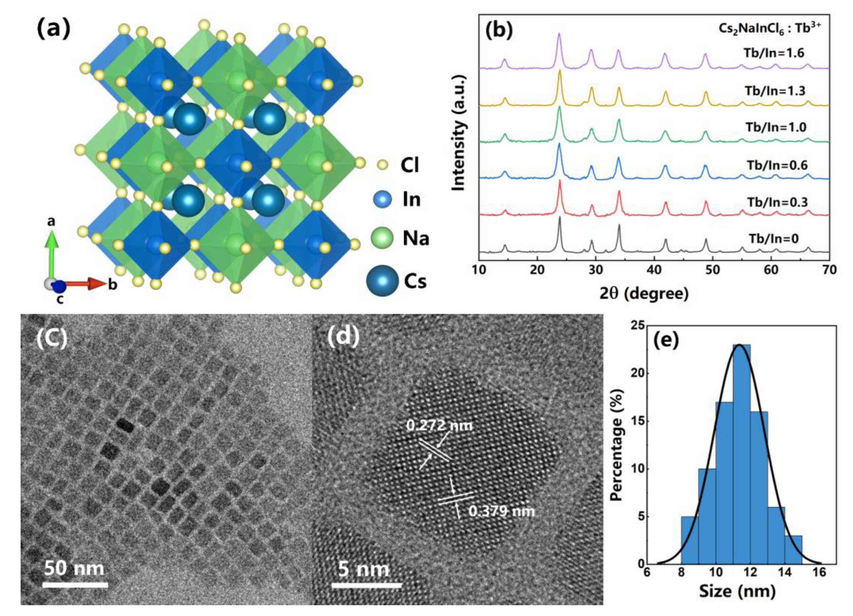
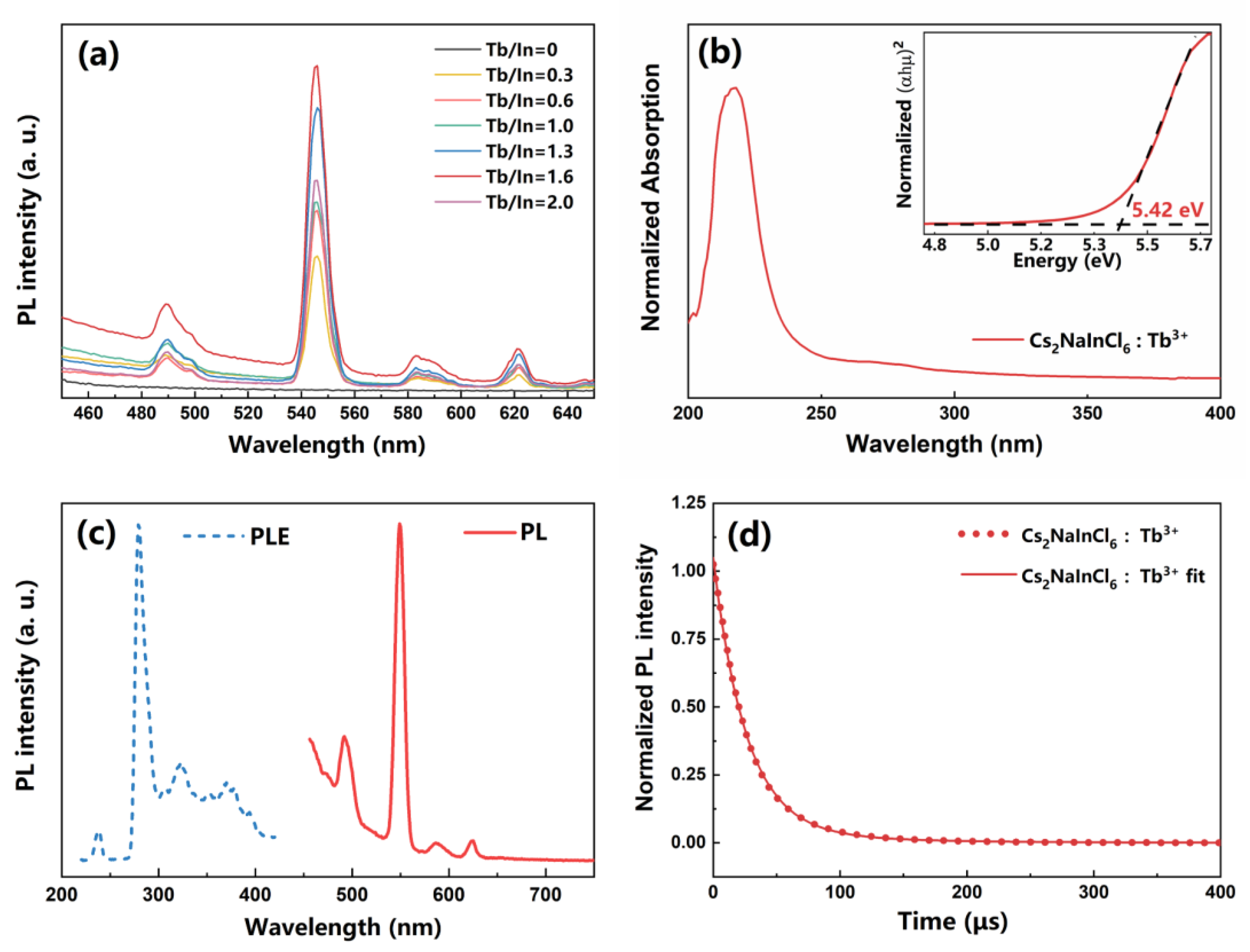
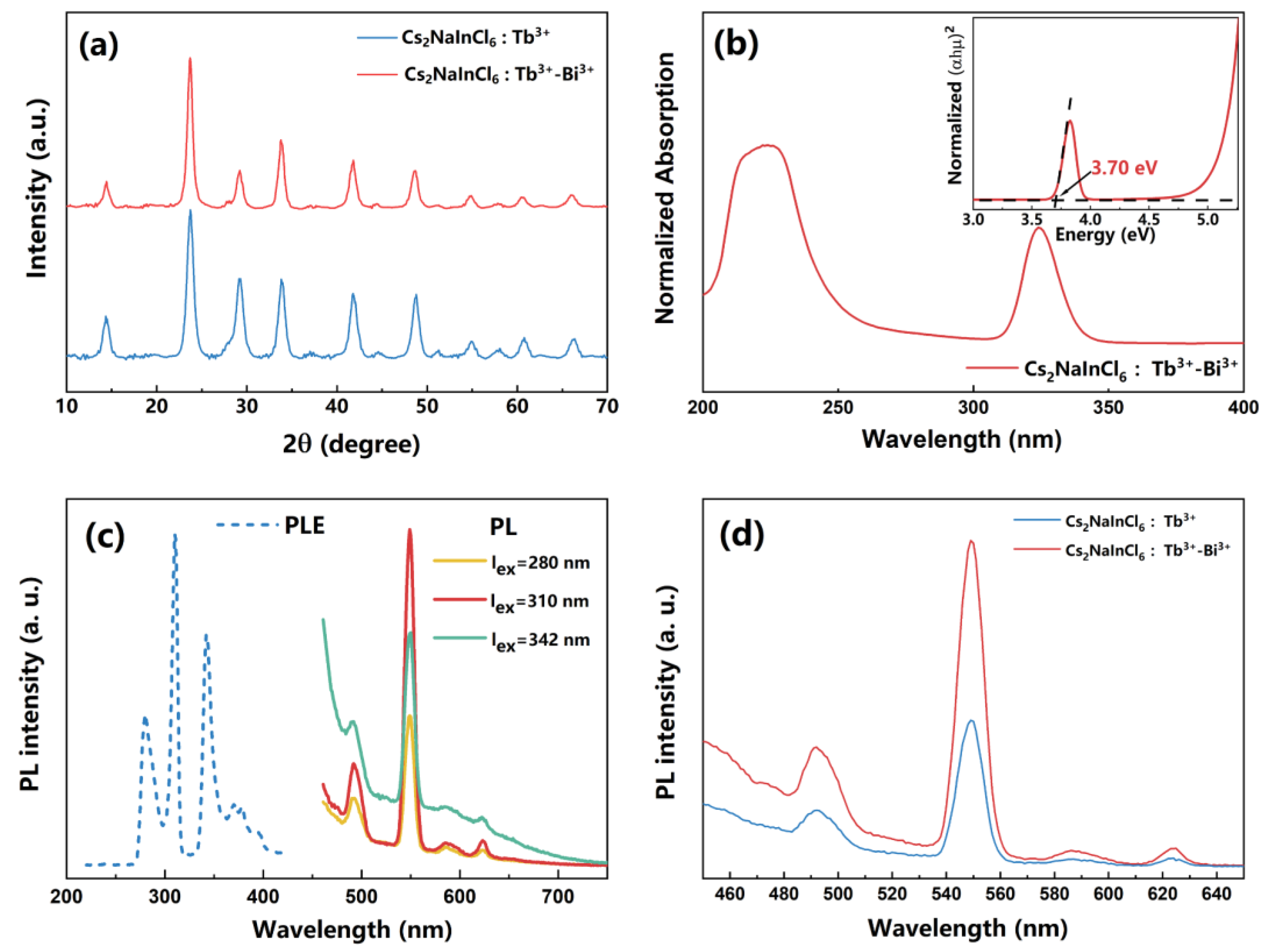
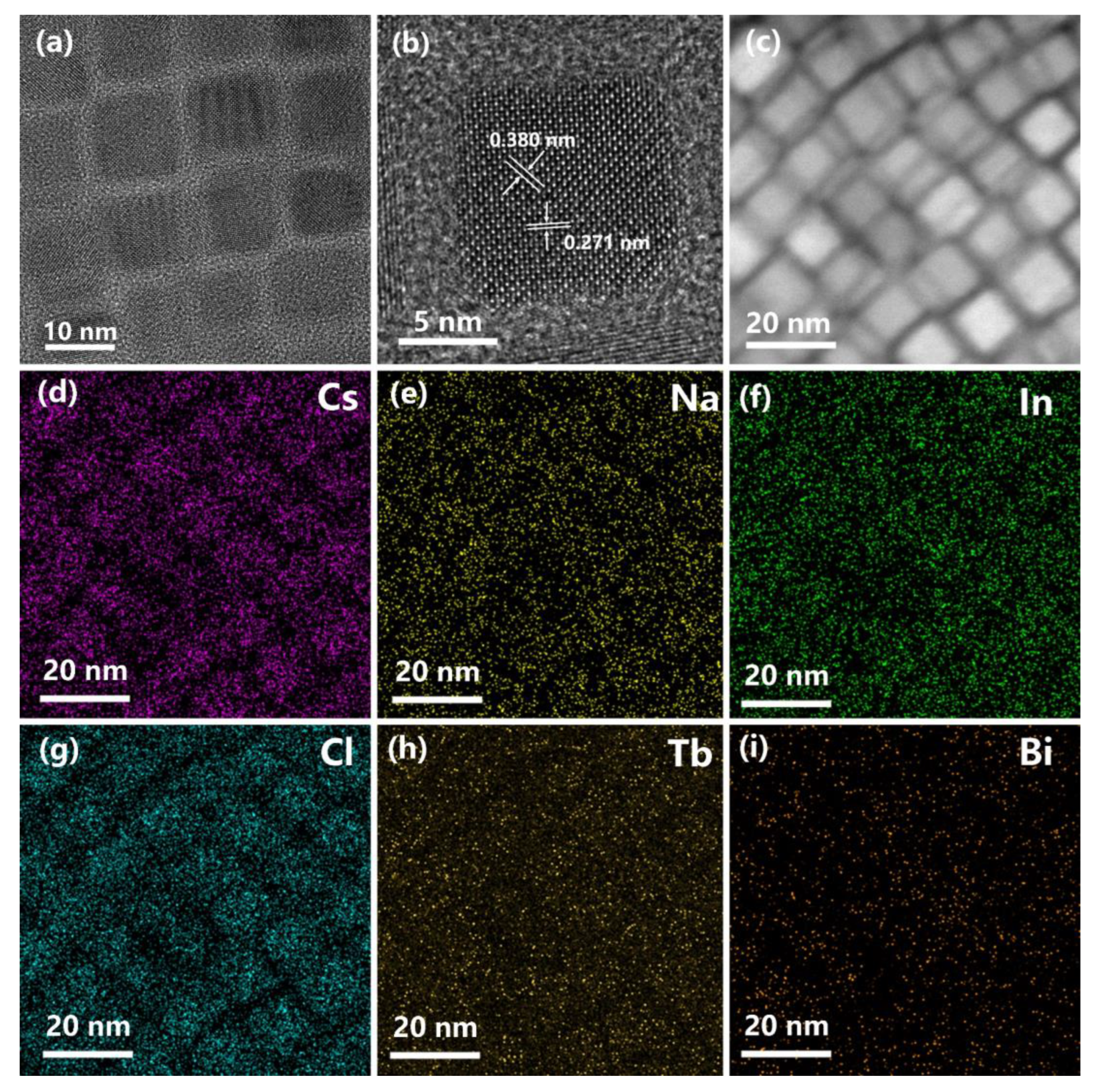
3. Results and Discussion

As shown in Figure 1a, the lattice structure of the Cs2NaInCl6 DP NCs crystallizes in a highly symmetric cubic structure (F m - 3m space group). Corner-connected [NaCl₆]5− and [InCl₆]3− octahedrons construct a 3D framework with Cs+ inserted in the octahedron’s cavities [31,32]. Figure 1b shows the PXRD patterns of the undoped and Tb3+-doped Cs2NaInCl6 DP NCs. The XRD peaks of the undoped Cs2NaInCl6 NCs at 2θ values of 14.4°, 23.8°, 28.1°, 29.3°, 34.0°, 41.9°, 48.9°, and 55.0° correspond to (111), (220), (311), (222), (400), (422), (440), and (620) lattice planes, respectively [33,34]. There is no detectable impurity phase in the doped NCs, implying that no phase separation occurred and the lattice structure remains unchanged. The actual doping concentrations in these samples are far lower than the feeding ratios revealed by the ICP-OES measurements (Table 1). Tb3+ ions are considered to replace In3+ ions in the crystalline lattice of Cs2NaInCl6 DP NCs [34,35,36]. The EDS result indicates that the molar ratio of major elements in Cs2NaInCl6 NCs is close to the ratio of 2:1:1:6 (Table 2). As shown in Figure 1c, the TEM image shows that the cubic-shaped Tb3+-doped Cs2NaInCl6 DP NCs are evenly distributed with an average size of about 11 nm. The high-resolution TEM (HRTEM) picture of Tb3+-doped NCs demonstrates excellent crystallinity with 0.272 nm and 0.379 nm lattice spacing values matched to the (400) and (220) crystal planes (Figure 1d).
The optical properties of the Tb3+-doped Cs2NaInCl6 DP NCs were investigated using steady-state PL and absorption spectra. The PL spectra under 280 nm excitation for Cs2NaInCl6 NCs with different Tb3+ doping ratios are shown in Figure 2a. The Tb3+-doped Cs2NaInCl6 NCs exhibit a major narrow green PL peak at 544 nm derived from the transition of Tb3+ 5D47F5, with three other small emission peaks at 490 nm, 583 nm, and 622 nm derived from the transitions of Tb3+ 5D47F6, 5D47F4, and 5D47F3 [21,37]. The PL intensity increases dramatically when the feeding ratio of doping agents is increased, while the peak location stays constant. The optimum Tb/In atomic feeding ratio is 1.6. After further increasing the Tb3+ doping amount, the PL intensity drops due to the concentration quenching effect. For clarity, the following discussion will focus on the optimal doping ratio samples. In the diffuse reflection absorption spectra (Figure 2b), a major absorption peak at 217 nm is observed for the Tb3+-doped NCs. The corresponding Tauc plot exhibits a wide band gap of 5.42 eV. The PLE and PL spectra of the Tb3+-doped NCs are shown in Figure 2c. A major green emission peak at 550 nm with a large Stokes shift of 270 nm is observed. The narrow green emission should be attributed to the characteristic emission of Tb3+ [21,37], while the undoped NCs are non-luminous, which indicates that Tb3+ ions are excited via energy transfer channels from the Cs2NaInCl6 host to Tb3+ ions. The photophysical properties of the Tb3+-doped NCs were investigated using transient PL spectra. As shown in Figure 2d, the PL lifetime of the Tb3+-doped NCs is fitted with exponential function with an extremely long lifetime (τ = 62 μs), which is attributed to the recombination process of excited Tb3+ ions involving an energy transfer from the Cs2NaInCl6 host to excite Tb3+ ions.
The use of a co-doping strategy to modify the PL properties of metal halide DPs has attracted a great deal of attention [23,24,25,26]. The trivalent Bi3+ cations are chosen for co-doping with Tb3+ ions for Cs2NaInCl6 DP NCs. The PXRD patterns of the Tb3+-Bi3+-co-doped Cs2NaInCl6 NCs are shown in Figure 3a. The XRD patterns of Tb3+-Bi3+-co-doped NCs are similar to those of Tb3+-singly-doped NCs, indicating that the lattice structure is not significantly altered with an additional 5% Bi3+ dopant. The TEM image of the Tb3+-Bi3+-co-doped NCs is shown in Figure 4a. The HRTEM image of the Tb3+-Bi3+-co-doped NCs shows excellent crystallinity with lattice spacing values of 0.271 nm and 0.380 nm matching to the (400) and (220) crystal planes (Figure 4b), indicating that the trace Bi3+ dopant does not significantly change the lattice distance. The mixing of Bi3+ and In3+ trivalent ions is considered to be random in the B’-site in the crystalline lattice [31]. The EDS element mappings show that the Cs, Na, In, Cl, Tb, and Bi elements are homogeneously distributed in the NCs, indicating the character of a single-phase compound (Figure 4d–i).
The absorption spectra of the Tb3+-Bi3+-co-doped NCs are shown in Figure 3b. Except for the major absorption peak at 223 nm, another absorption peak is detected at 325 nm, which should be attributed to the correlated 6s2-6s16p1 transitions of Bi3+ ions. The insert Tauc plot shows a band gap of 3.70 eV for the Tb3+-Bi3+-co-doped NCs, indicating that Bi3+ co-doping can lower the band gap of the DP NCs because the energy can transfer directly from the Bi3+ ions to the Tb3+ ions. As shown in Figure 3c, the PLE spectrum of Tb3+-Bi3+-co-doped NCs shows three PLE peaks at 280 nm, 310 nm, and 342 nm, which is different from the Tb3+-singly-doped NCs. Similar PL emission peaks at 549 nm with large Stokes shifts of 269 nm, 238 nm, and 206 nm are observed. With Bi3+ co-doping, which decreased the energy of absorbed photons, the samples are not only directly excited at 280 nm but are also excited at 310 nm and 342 nm. The latter obtain a higher PL intensity because partial Tb3+ ions in co-doped NCs are excited through more efficient energy transfer channels from the Bi3+ to the Tb3+ ions, consistent with the previous reports [16,22]. The PL spectra of the Tb+-singly-doped and Tb3+-Bi3+-co-doped Cs2NaInCl6 NCs are shown in Figure 3d. The higher PL intensity of Tb3+-Bi3+-co-doped NCs than that of Tb3+-singly-doped NCs demonstrates that the energy transfer channel built by introducing Bi3+ ions is more favorable for the highly efficient luminescence of Tb3+ ions than the intrinsic excitation band.

4. Conclusions

In conclusion, we report the Tb3+ and Bi3+ doping of Cs2NaInCl6 DP NCs for narrow green PL. The Tb3+-doped Cs2NaInCl6 DP NCs exhibit a major narrow green PL peak at 544 nm, derived from the transition of Tb3+ 5D47F5, with three other small emission peaks at 490 nm, 583 nm, and 622 nm derived from the transitions of Tb3+ 5D47F6, 5D47F4, and 5D47F3. The ultra-long PL lifetime of about 62 μs corresponds to the recombination process of excited Tb3+ ions, involving an energy transfer from the Cs2NaInCl6 host to excite Tb3+ ions. The additional two stronger PLE peaks at 310 nm and 342 nm caused by further Bi3+ co-doping indicate that partial Tb3+ ions in Tb3+-Bi3+-co-doped NCs are not only directly excited at 280 nm but are also more efficiently excited through energy transfer channels from the Bi3+ to the Tb3+ ions. The emission intensity of Tb3+-Bi3+-co-doped NCs is much higher than that of Tb3+-singly-doped NCs, indicating that introducing Bi3+ ions is more favorable for the highly efficient luminescence of Tb3+ ions by providing more efficient energy transfer channels. This work provides an effective method for producing lead-free halide DPs with excellent optical properties, and this mechanism has great potential for tailoring the optical properties of DPs.

Author Contributions

Conceptualization, Y.Y., W.Z., P.H., H.L. and K.Z.; writing—original draft preparation, Y.Y.; formal analysis, Y.Y. and W.Z.; investigation, W.Z. and C.L.; writing—review and editing, P.H., H.L. and K.Z.; funding acquisition, Y.Y., P.H., H.L. and K.Z. All authors have read and agreed to the published version of the manuscript.

Funding

This research was funded by the National Natural Science Foundation of China (grant nos. 52002182, 12204237, and 62105154), the China Postdoctoral Science Foundation (grant no. 2022M711898), the Natural Science Foundation of Jiangsu Province (grant nos. BK20220922 and BK20210324), and the Fundamental Research Funds for the Central Universities (grant no. 30922010319).

Data Availability Statement

The data presented in this study are available upon request from the corresponding author.

Conflicts of Interest

The authors declare no conflict of interest.

References

  1. Lee, M.M.; Teuscher, J.; Miyasaka, T.; Murakami, T.N.; Snaith, H.J. Efficient Hybrid Solar Cells Based on Meso-Superstructured Organometal Halide Perovskites. Science 2012, 338, 643–647. [Google Scholar] [CrossRef] [Green Version]
  2. Yang, Y.; Hoang, M.T.; Bhardwaj, A.; Wilhelm, M.; Mathur, S.; Wang, H. Perovskite Solar Cells Based Self-Charging Power Packs: Fundamentals, Applications and Challenges. Nano Energy 2022, 94, 106910. [Google Scholar] [CrossRef]
  3. Burschka, J.; Pellet, N.; Moon, S.-J.; Humphry-Baker, R.; Gao, P.; Nazeeruddin, M.K.; Graetzel, M. Sequential Deposition as a Route to High-Performance Perovskite-Sensitized Solar Cells. Nature 2013, 499, 316–319. [Google Scholar] [CrossRef]
  4. Yuan, M.; Quan, L.N.; Comin, R.; Walters, G.; Sabatini, R.; Voznyy, O.; Hoogland, S.; Zhao, Y.; Beauregard, E.M.; Kanjanaboos, P.; et al. Perovskite Energy Funnels for Efficient Light-Emitting Diodes. Nat. Nanotechnol. 2016, 11, 872–877. [Google Scholar] [CrossRef] [PubMed]
  5. Lin, K.; Xing, J.; Quan, L.N.; de Arquer, F.P.G.; Gong, X.; Lu, J.; Xie, L.; Zhao, W.; Zhang, D.; Yan, C.; et al. Perovskite Light-Emitting Diodes with External Quantum Efficiency Exceeding 20 Percent. Nature 2018, 562, 245–248. [Google Scholar] [CrossRef]
  6. Wang, Y.; Li, X.; Song, J.; Xiao, L.; Zeng, H.; Sun, H. All-Inorganic Colloidal Perovskite Quantum Dots: A New Class of Lasing Materials with Favorable Characteristics. Adv. Mater. 2015, 27, 7101–7108. [Google Scholar] [CrossRef] [PubMed]
  7. Sutherland, B.R.; Sargent, E.H. Perovskite Photonic Sources. Nat. Photonics 2016, 10, 295–302. [Google Scholar] [CrossRef]
  8. Giustino, F.; Snaith, H.J. Toward Lead-Free Perovskite Solar Cells. ACS Energy Lett. 2016, 1, 1233–1240. [Google Scholar] [CrossRef] [Green Version]
  9. Liang, L.; Gao, P. Lead-Free Hybrid Perovskite Absorbers for Viable Application: Can We Eat the Cake and Have It Too? Adv. Sci. 2018, 5, 1700331. [Google Scholar] [CrossRef]
  10. Wu, X.; Song, W.; Li, Q.; Zhao, X.; He, D.; Quan, Z. Synthesis of Lead-Free CsGeI2 Perovskite Colloidal Nanocrystals and Electron Beam-Induced Transformations. Chem. Asian J. 2018, 13, 1654–1659. [Google Scholar] [CrossRef]
  11. Jellicoe, T.C.; Richter, J.M.; Glass, H.F.J.; Tabachnyk, M.; Brady, R.; Dutton, S.E.; Rao, A.; Friend, R.H.; Credgington, D.; Greenham, N.C.; et al. Synthesis and Optical Properties of Lead-Free Cesium Tin Halide Perovskite Nanocrystals. J. Am. Chem. Soc. 2016, 138, 2941–2944. [Google Scholar] [CrossRef] [Green Version]
  12. Du, K.; Meng, W.; Wang, X.; Yan, Y.; Mitzi, D.B. Bandgap Engineering of Lead-Free Double Perovskite Cs2AgBiBr6 through Trivalent Metal Alloying. Angew. Chem. Int. Ed. 2017, 56, 8158–8162. [Google Scholar] [CrossRef] [PubMed]
  13. Meng, W.; Wang, X.; Xiao, Z.; Wang, J.; Mitzi, D.B.; Yan, Y. Parity-Forbidden Transitions and Their Impact on the Optical Absorption Properties of Lead-Free Metal Halide Perovskites and Double Perovskites. J. Phys. Chem. Lett. 2017, 8, 2999–3007. [Google Scholar] [CrossRef] [PubMed] [Green Version]
  14. Karmakar, A.; Dodd, M.S.; Agnihotri, S.; Ravera, E.; Michaelis, V.K. Cu(II)-Doped Cs2SbAgCl6 Double Perovskite: A Lead-Free, Low-Bandgap Material. Chem. Mater. 2018, 30, 8280–8290. [Google Scholar] [CrossRef] [Green Version]
  15. Han, P.; Han, K. Recent Advances in All-Inorganic Lead-Free Three-Dimensional Halide Double Perovskite Nanocrystals. Energy Fuels 2021, 35, 18871–18887. [Google Scholar] [CrossRef]
  16. Li, S.; Hu, Q.; Luo, J.; Jin, T.; Liu, J.; Li, J.; Tan, Z.; Han, Y.; Zheng, Z.; Zhai, T.; et al. Self-Trapped Exciton to Dopant Energy Transfer in Rare Earth Doped Lead-Free Double Perovskite. Adv. Opt. Mater. 2019, 7, 1901098. [Google Scholar] [CrossRef]
  17. Chen, N.; Cai, T.; Li, W.; Hills-Kimball, K.; Yang, H.; Que, M.; Nagaoka, Y.; Liu, Z.; Yang, D.; Dong, A.; et al. Yb- and Mn-Doped Lead-Free Double Perovskite Cs2AgBiX6 (X = Cl, Br) Nanocrystals. ACS Appl. Mater. Interfaces 2019, 11, 16855–16863. [Google Scholar] [CrossRef]
  18. Mahor, Y.; Mir, W.J.; Nag, A. Synthesis and Near-Infrared Emission of Yb-Doped Cs2AgInCl6 Double Perovskite Microcrystals and Nanocrystals. J. Phys. Chem. C 2019, 123, 15787–15793. [Google Scholar] [CrossRef]
  19. Zeng, R.; Zhang, L.; Xue, Y.; Ke, B.; Zhao, Z.; Huang, D.; Wei, Q.; Zhou, W.; Zou, B. Highly Efficient Blue Emission from Self-Trapped Excitons in Stable Sb3+-Doped Cs2NaInCl6 Double Perovskites. J. Phys. Chem. Lett. 2020, 11, 2053–2061. [Google Scholar] [CrossRef]
  20. Li, H.; Tian, L.; Shi, Z.; Li, Y.; Li, C.; Feng, J.; Zhang, H. Double Perovskite Cs2NaInCl6 Nanocrystals with Intense Dual-Emission via Self-Trapped Exciton-to-Tb3+ Dopant Energy Transfer. J. Mater. Chem. C 2022, 10, 10609–10615. [Google Scholar] [CrossRef]
  21. Dong, H.; Sun, L.-D.; Yan, C.-H. Energy Transfer in Lanthanide Upconversion Studies for Extended Optical Applications. Chem. Soc. Rev. 2015, 44, 1608–1634. [Google Scholar] [CrossRef] [PubMed]
  22. Liu, Y.; Rong, X.; Li, M.; Molokeev, M.S.; Zhao, J.; Xia, Z. Incorporating Rare-Earth Terbium(III) Ions into Cs2AgInCl6:Bi Nanocrystals toward Tunable Photoluminescence. Angew. Chem. Int. Ed. 2020, 59, 11634–11640. [Google Scholar] [CrossRef] [PubMed]
  23. Arfin, H.; Kshirsagar, A.S.; Kaur, J.; Mondal, B.; Xia, Z.; Chakraborty, S.; Nag, A. ns2 Electron (Bi3+ and Sb3+) Doping in Lead-Free Metal Halide Perovskite Derivatives. Chem. Mater. 2020, 32, 10255–10267. [Google Scholar] [CrossRef]
  24. Liu, X.; Xu, X.; Li, B.; Yang, L.; Li, Q.; Jiang, H.; Xu, D. Tunable Dual-Emission in Monodispersed Sb3+/Mn2+ Codoped Cs2NaInCl6 Perovskite Nanocrystals through an Energy Transfer Process. Small 2020, 16, 2002547. [Google Scholar] [CrossRef]
  25. Wang, C.-Y.; Liang, P.; Xie, R.-J.; Yao, Y.; Liu, P.; Yang, Y.; Hu, J.; Shao, L.; Sun, X.W.; Kang, F.; et al. Highly Efficient Lead-Free (Bi,Ce)-Codoped Cs2Ag0.4Na0.6 InCl6 Double Perovskites for White Light-Emitting Diodes. Chem. Mater. 2020, 32, 7814–7821. [Google Scholar] [CrossRef]
  26. Arfin, H.; Kaur, J.; Sheikh, T.; Chakraborty, S.; Nag, A. Bi3+-Er3+ and Bi3+-Yb3+ Codoped Cs2 AgInCl6 Double Perovskite Near-Infrared Emitters. Angew. Chem. Int. Ed. 2020, 59, 11307–11311. [Google Scholar] [CrossRef] [PubMed]
  27. Han, P.; Mao, X.; Yang, S.; Zhang, F.; Yang, B.; Wei, D.; Deng, W.; Han, K. Lead-Free Sodium–Indium Double Perovskite Nanocrystals through Doping Silver Cations for Bright Yellow Emission. Angew. Chem. Int. Ed. 2019, 58, 17231–17235. [Google Scholar] [CrossRef] [PubMed]
  28. Locardi, F.; Cirignano, M.; Baranov, D.; Dang, Z.; Prato, M.; Drago, F.; Ferretti, M.; Pinchetti, V.; Fanciulli, M.; Brovelli, S.; et al. Colloidal Synthesis of Double Perovskite Cs2AgInCl6 and Mn-Doped Cs2AgInCl6 Nanocrystals. J. Am. Chem. Soc. 2018, 140, 12989–12995. [Google Scholar] [CrossRef]
  29. Han, P.; Zhang, X.; Luo, C.; Zhou, W.; Yang, S.; Zhao, J.; Deng, W.; Han, K. Manganese-Doped, Lead-Free Double Perovskite Nanocrystals for Bright Orange-Red Emission. ACS Cent. Sci. 2020, 6, 566–572. [Google Scholar] [CrossRef] [Green Version]
  30. Zhou, W.; Han, P.; Luo, C.; Li, C.; Hou, J.; Yu, Y.; Lu, R. Band-Gap and Dimensional Engineering in Lead-Free Inorganic Halide Double Perovskite Cs2Cu1-xAg2xSb2Cl12 Single Crystals and Nanocrystals. Front. Mater. 2022, 9, 855950. [Google Scholar] [CrossRef]
  31. Zhou, J.; Rong, X.; Zhang, P.; Molokeev, M.S.; Wei, P.; Liu, Q.; Zhang, X.; Xia, Z. Manipulation of Bi3+/In3+ Transmutation and Mn2+-Doping Effect on the Structure and Optical Properties of Double Perovskite Cs2NaBi1−xInxCl6. Adv. Opt. Mater. 2019, 7, 1801435. [Google Scholar] [CrossRef] [Green Version]
  32. Gray, M.B.; Hariyani, S.; Strom, T.A.; Majher, J.D.; Brgoch, J.; Woodward, P.M. High-Efficiency Blue Photoluminescence in the Cs2NaInCl6:Sb3+ Double Perovskite Phosphor. J. Mater. Chem. C 2020, 8, 6797–6803. [Google Scholar] [CrossRef]
  33. Chen, L.; Yang, W.; Fu, H.; Liu, W.; Shao, G.; Tang, B.; Zheng, J. Mn2+-Doped Cs2NaInCl6 Double Perovskites and Their Photoluminescence Properties. J. Mater. Sci. 2021, 56, 8048–8059. [Google Scholar] [CrossRef]
  34. Ahmad, R.; Zdražil, L.; Kalytchuk, S.; Naldoni, A.; Rogach, A.L.; Schmuki, P.; Zboril, R.; Kment, Š. Uncovering the Role of Trioctylphosphine on Colloidal and Emission Stability of Sb-Alloyed Cs2NaInCl6 Double Perovskite Nanocrystals. ACS Appl. Mater. Interfaces 2021, 13, 47845–47859. [Google Scholar] [CrossRef] [PubMed]
  35. Noculak, A.; Morad, V.; McCall, K.M.; Yakunin, S.; Shynkarenko, Y.; Wörle, M.; Kovalenko, M.V. Bright Blue and Green Luminescence of Sb(III) in Double Perovskite Cs2MInCl6 (M = Na, K) Matrices. Chem. Mater. 2020, 32, 5118–5124. [Google Scholar] [CrossRef] [PubMed]
  36. Nie, J.; Li, H.; Fang, S.; Zhou, B.; Liu, Z.; Chen, F.; Wang, Y.; Shi, Y. Efficient Red Photoluminescence in Holmium-Doped Cs2NaInCl6 Double Perovskite. Cell Rep. Phys. Sci. 2022, 3, 100820. [Google Scholar] [CrossRef]
  37. Marin, R.; Jaque, D. Doping Lanthanide Ions in Colloidal Semiconductor Nanocrystals for Brighter Photoluminescence. Chem. Rev. 2021, 121, 1425–1462. [Google Scholar] [CrossRef]
Figure 1. (a) Cs2NaInCl6 NCs lattice structure, with yellow, blue, and green spheres representing Cl, In, and Na atoms, and bigger blue spheres representing Cs atoms. (b) PXRD patterns of the undoped and Tb3+-doped Cs2NaInCl6 DP NCs. (c) TEM and (d) HRTEM images of Tb3+-doped Cs2NaInCl6 DP NCs. (e) Histogram of the size distribution of Tb3+-doped Cs2NaInCl6 NCs.
Nanomaterials 13 00549 g001
Figure 2. (a) PL spectra under 280 nm excitation for Cs2NaInCl6 NCs with different Tb3+ doping ratios. (b) Diffuse reflection absorption spectrum; insert shows the corresponding Tauc plots of Tb3+-doped Cs2NaInCl6 NCs. (c) PLE and PL, (d) time-resolved PL spectra of the Tb3+-doped Cs2NaInCl6 NCs with fitting curves.
Nanomaterials 13 00549 g002
Figure 3. (a) PXRD patterns of the Tb3+-singly-doped and Tb3+-Bi3+-co-doped Cs2NaInCl6 NCs. (b) Diffuse reflection absorption spectrum; insert shows the corresponding Tauc plots of the Tb3+-Bi3+-co-doped Cs2NaInCl6 NCs. (c) PLE and PL spectra of the Tb3+-Bi3+-co-doped Cs2NaInCl6 NCs. (d) PL spectra of the Tb3+-singly-doped and Tb3+-Bi3+-co-doped Cs2NaInCl6 NCs.
Nanomaterials 13 00549 g003
Figure 4. (a) TEM, (b) HRTEM, (c) high-angle annular dark field (HAADF) images of the Tb3+-Bi3+-co-doped Cs2NaInCl6 NCs. (di) EDS elemental mappings of Cs, Na, In, Cl, Tb, and Bi localized in the Tb3+-Bi3+-co-doped Cs2NaInCl6 NCs.
Nanomaterials 13 00549 g004
Table 1. The ICP-OES results of different feed ratios of Tb3+-doped Cs2NaInCl6 DP NCs.
Cs2NaInCl6:Tb3+
Feeding Ratios
In (mg/L)Tb (mg/L)In (%)Tb (%)Tb/In
Actual Ratios
Tb/In = 0.317.680.03515.370.0220.001432
Tb/In = 0.613.220.04911.500.0310.002681
Tb/In = 1.017.330.10615.070.0670.004424
Tb/In = 1.313.630.09711.850.0610.005147
Tb/In = 1.616.670.12114.500.0760.005250
Tb/In = 2.034.630.28530.110.1790.005952
Table 2. The EDS results of Tb3+-doped Cs2NaInCl6 DP NCs.
ElementWeight%Atomic%
Na3.8310.19
Cl34.9360.18
In20.9911.16
Cs39.9518.36
Tb0.290.11
Disclaimer/Publisher’s Note: The statements, opinions and data contained in all publications are solely those of the individual author(s) and contributor(s) and not of MDPI and/or the editor(s). MDPI and/or the editor(s) disclaim responsibility for any injury to people or property resulting from any ideas, methods, instructions or products referred to in the content.

