

Optical Optimization of Tandem Solar Cells: A Systematic Review for Enhanced Power Conversion

Abstract
:1. Introduction
- RQ1. What are the current optical designs used in different TSCs, and what are their potential benefits?
- RQ2. What are the different techniques used for searching for an optimal optical design for TSCs in the literature?
- RQ3. What are the current learning-based methods for the optical design of TSCs?
- RQ4. What are the key challenges faced by different optical designs for TSCs?
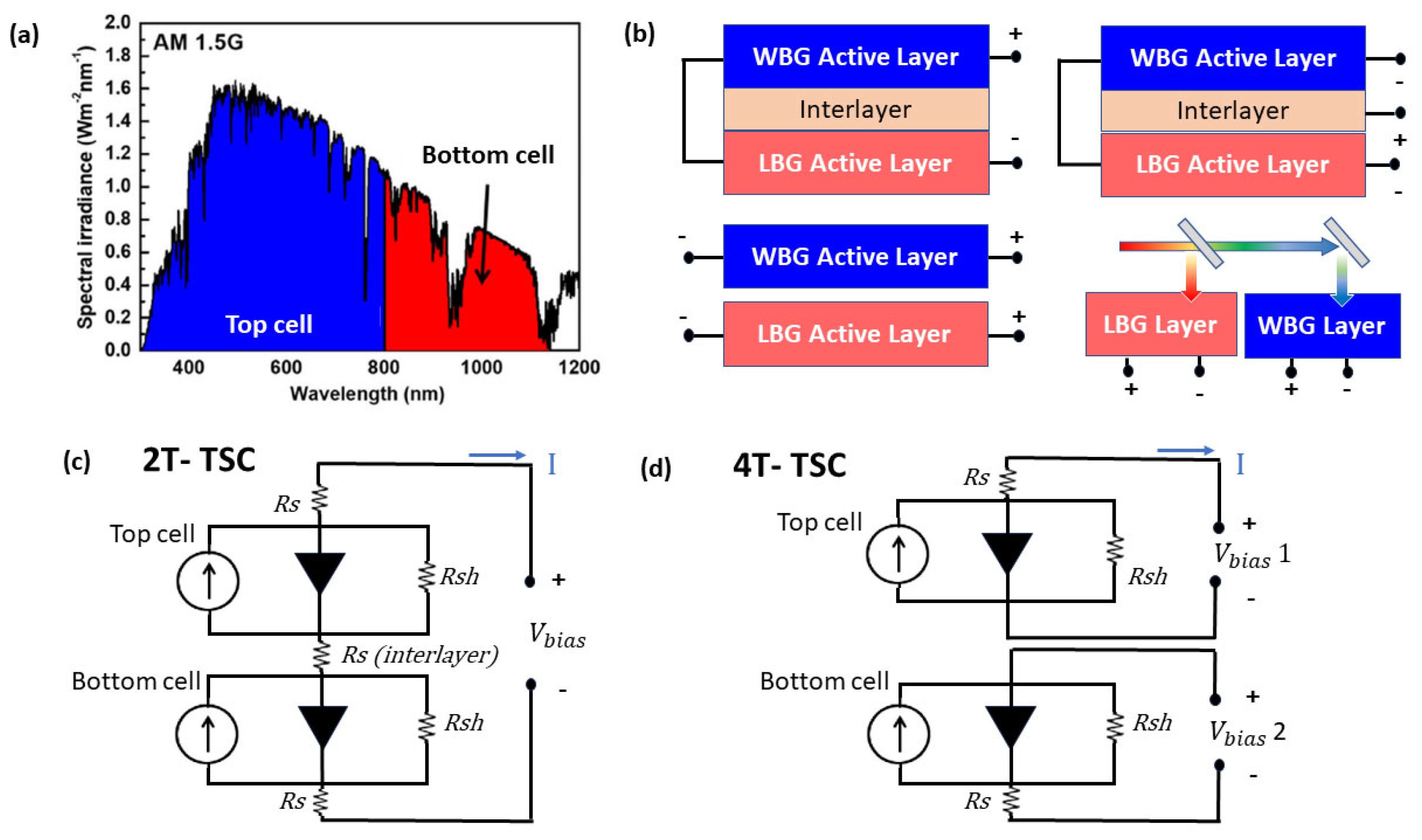
2. Types of TSC
- Monolithic two-terminal (2T) TSC
- Four-terminal (4T) TSC
2.1. Two-Terminal (2T)-TSC

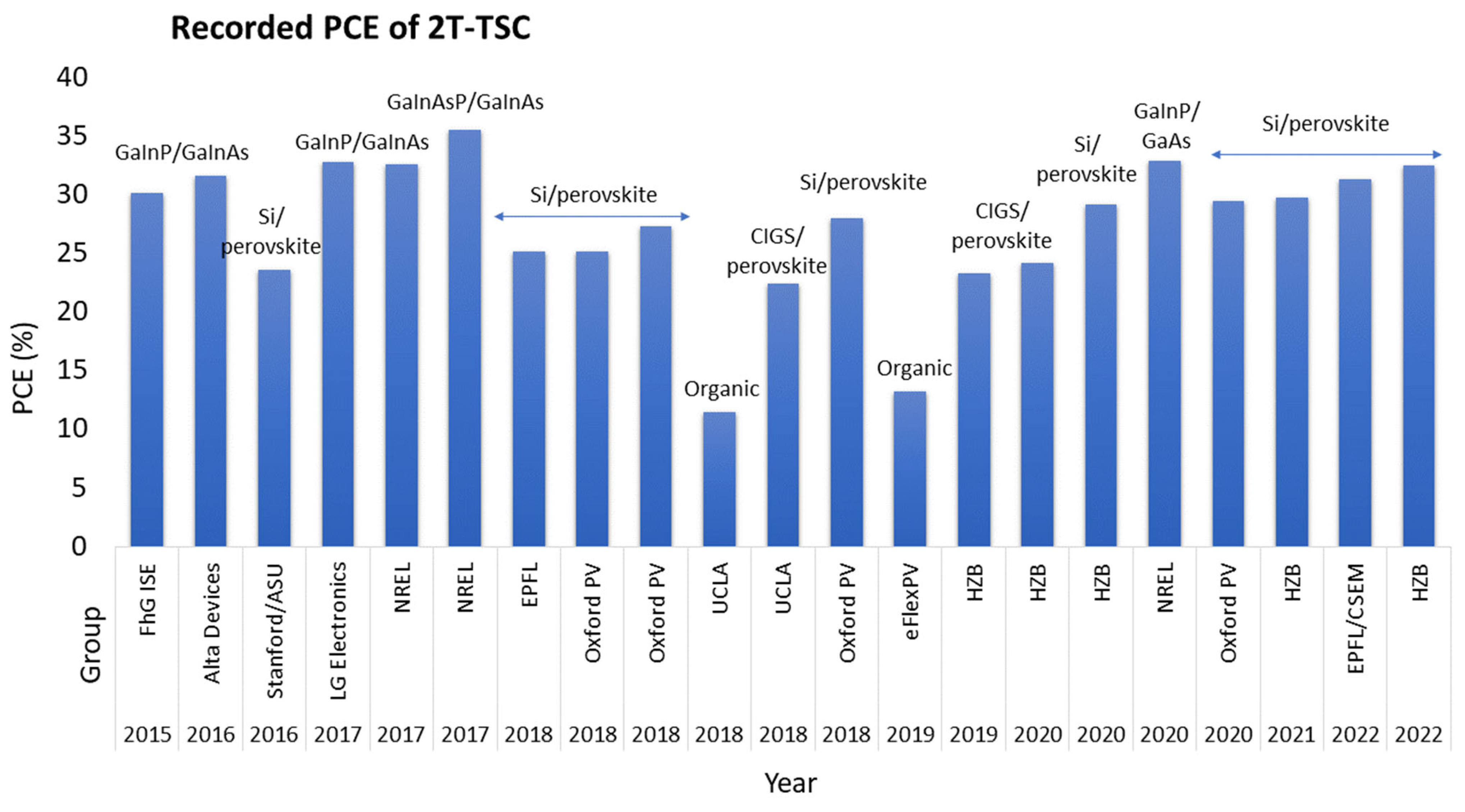
| Year | 2T-Monolithic TSC Type | Group(s) | PCE (%) | Area (cm2) | VOC (V) | Jsc (mA/cm2) | FF (%) | Ref. |
|---|---|---|---|---|---|---|---|---|
| 2015 | GaInP/GaInAs | Fraunhofer ISE | 30.2 | 4 | - | - | - | [38] |
| 2016 | GaInP/GaAs | Alta Devices | 31.6 | 0.999 | 2.538 | 14.18 | 87.7 | [39] |
| 2016 | Perovskite/Si | Stanford/ASU | 23.6 | 0.99 | 1.651 | 18.09 | 79 | [38] |
| 2017 | GaInP/GaAs | LG Electronics | 32.8 | 1 | 2.568 | 14.56 | 87.7 | [41] |
| 2017 | GaInP/GaAs | NREL | 32.6 | 0.248 | 2.024 | 19.51 | 82.5 | [40] |
| 2017 | GaInAsP/GaInAs | NREL | 35.5 | 0.10031 | - | - | - | [40] |
| 2018 | Perovskite/Si | EPFL | 25.2 | 1.419 | 1.787 | 19.53 | 72.3 | [42] |
| 2018 | Perovskite/Si | Oxford PV/Oxford/HZB | 25.2 | 1.088 | 1.793 | 19.02 | 73.8 | [40] |
| 2018 | Perovskite/Si | Oxford PV | 27.3 | 1.09 | 1.813 | 19.99 | 75.4 | [40] |
| 2018 | Organic TSC | UCLA | 11.5 | 0.06 | 1.56 | 10.07 | - | [40] |
| 2018 | Perovskite/CIGS | UCLA | 22.4 | 0.042 | 1.774 | 17.3 | 73.1 | [40] |
| 2018 | Perovskite/Si | Oxford PV | 28 | 1.03 | 1.802 | 19.75 | 78.7 | [43] |
| 2019 | Organic TSC | SCUT/eFlexPV | 13.2 | 0.041 | 1.61 | 11.22 | 73 | [40] |
| 2019 | Perovskite/CIGS | HZB | 23.3 | 1.035 | 1.683 | 19.17 | 72.1 | [40] |
| 2020 | Perovskite/CIGS | HZB | 24.2 | 1.045 | 1.768 | 19.24 | 72.9 | [40] |
| 2020 | Perovskite/Si | HZB | 29.15 | 1.06 | 1.897 | 19.75 | 77.8 | [44] |
| 2020 | GaInP/GaAs | NREL | 32.9 | 0.25 | 2.5 | 15.36 | 85.7 | [40] |
| 2020 | Perovskite/Si | Oxford PV | 29.5 | 1.121 | 1.884 | 20.26 | 77.3 | [40] |
| 2021 | Perovskite/Si | HZB | 29.8 | 1.016 | 1.8 | - | - | [40] |
| 2022 | Perovskite/Si | EPFL/CSEM | 31.3 | 1.1677 | 1.9131 | 20.473 | 79.8 | [40] |
| 2022 | Perovskite/Si | HZB | 32.5 | 1.014 | 1.9798 | 20.24 | 81.2 | [40] |
2.2. Four-Terminal (4T) TSCs
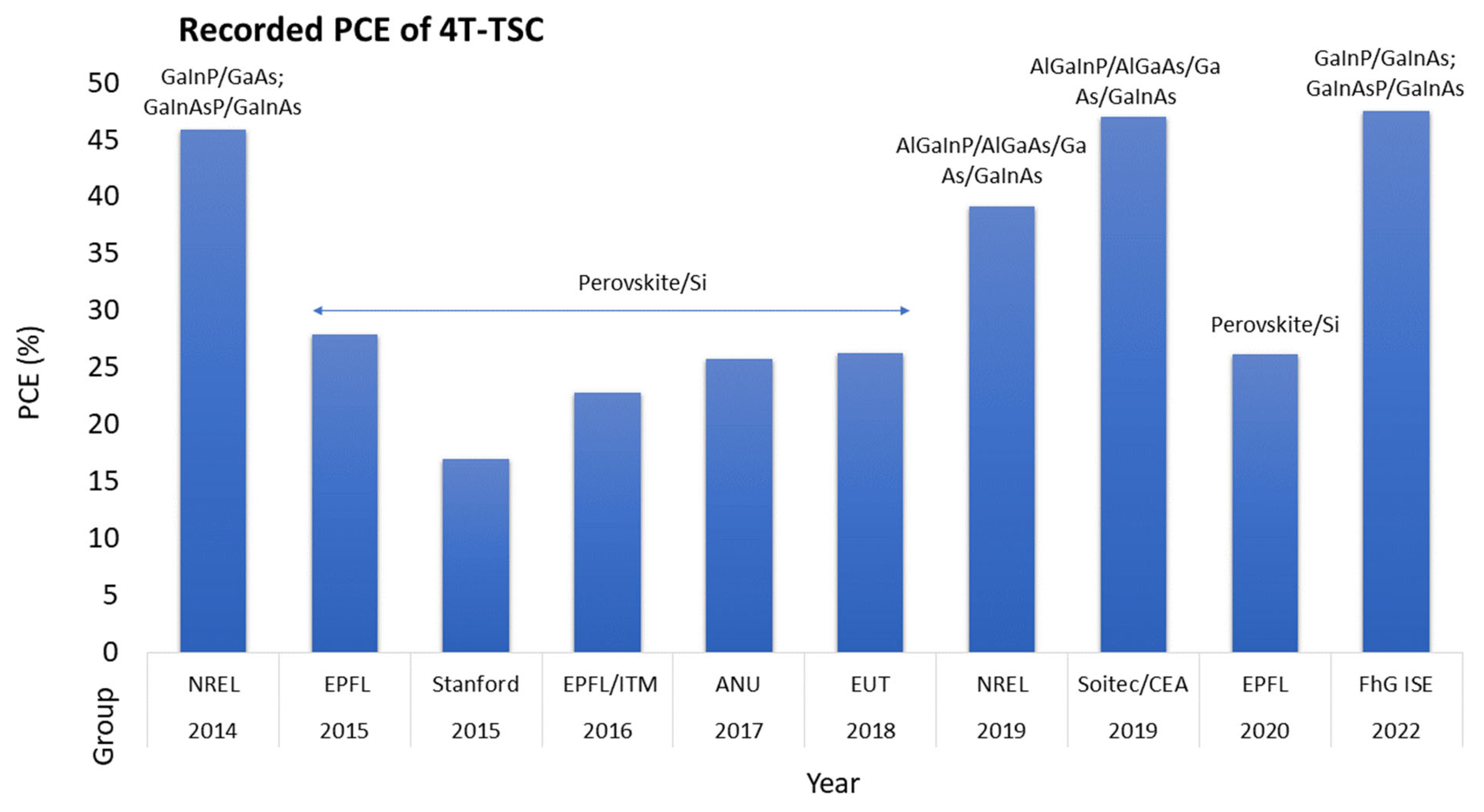
| Year | 4T Monolithic TSC Type | PCE (%) | Area (cm2) | VOC (V) | Jsc (mA/cm2) | FF (%) | Ref. |
|---|---|---|---|---|---|---|---|
| 2014 | 4T GaInP/GaAs; GaInAsP/GaInAs | 46 | 0.052 | - | - | - | [40] |
| 2015 | 4T Heterojunction Si/perovskite | 28 | 0.25 | 0.21 | 14.5 | 76 | [45] |
| 2015 | 4T Si/perovskite | 17 | 0.39 | 0.64 | 28 | 66 | [51] |
| 2016 | 4T Si/perovskite | 22.8 | 0.25 | 1.6 | 34.8 | 79 | [52] |
| 2017 | 4T Si/perovskite | 25.8 | 0.17 | 1.7 | 38.2 | 80 | [53] |
| 2018 | 4T Si/perovskite | 26.3 | 0.09 | 1.7 | 37.1 | 80 | [55] |
| 2019 | 4T AlGaInP/AlGaAs/GaAs/GaInAs | 39.2 | 0.09 | 5.55 | 8.46 | 83 | [40] |
| 2019 | 4T AlGaInP/AlGaAs/GaAs/GaInAs | 47.1 | 0.09 | - | - | - | [40] |
| 2020 | 4T Si/perovskite | 26.2 | 0.05 | 1.7 | 35.3 | 80.2 | [59] |
| 2022 | 4T GaInP/GaInAs; GaInAsP/GaInAs | 47.6 | 0.04 | - | - | - | [40] |
3. Fundamental Aspects
3.1. Nanostructure and Materials
3.2. Optimization
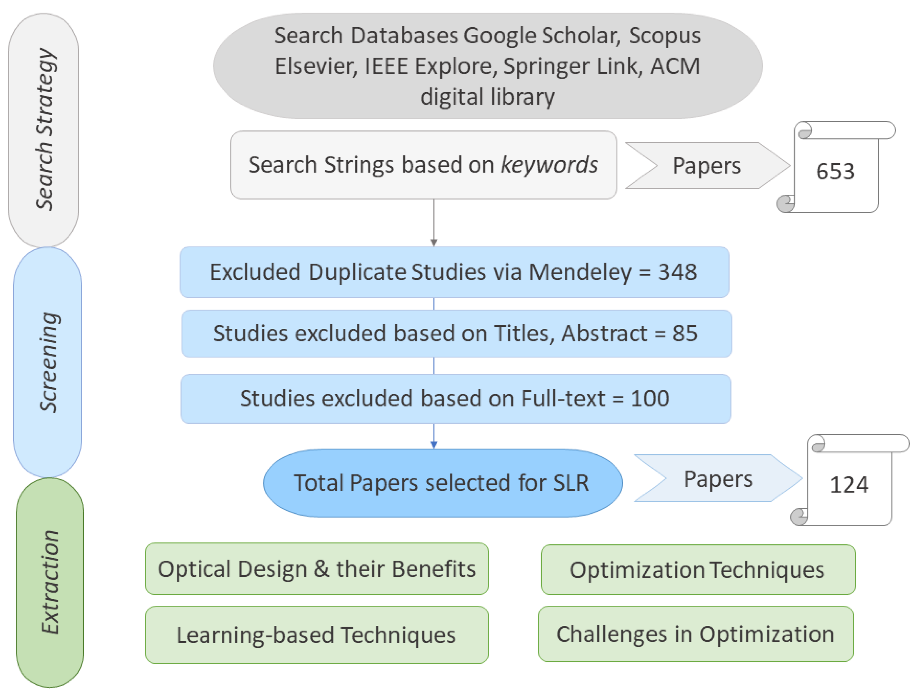
4. SLR Methodology
4.1. Search Strategy and Screening
4.2. Data Extraction
5. SLR Results
5.1. Publication Source and Citation Overview
5.2. Temporal Overview
6. Research Question Results
6.1. What Are the Current Optical Designs Used in Different TSCs, and What Are Their Potential Benefits? (RQ1)
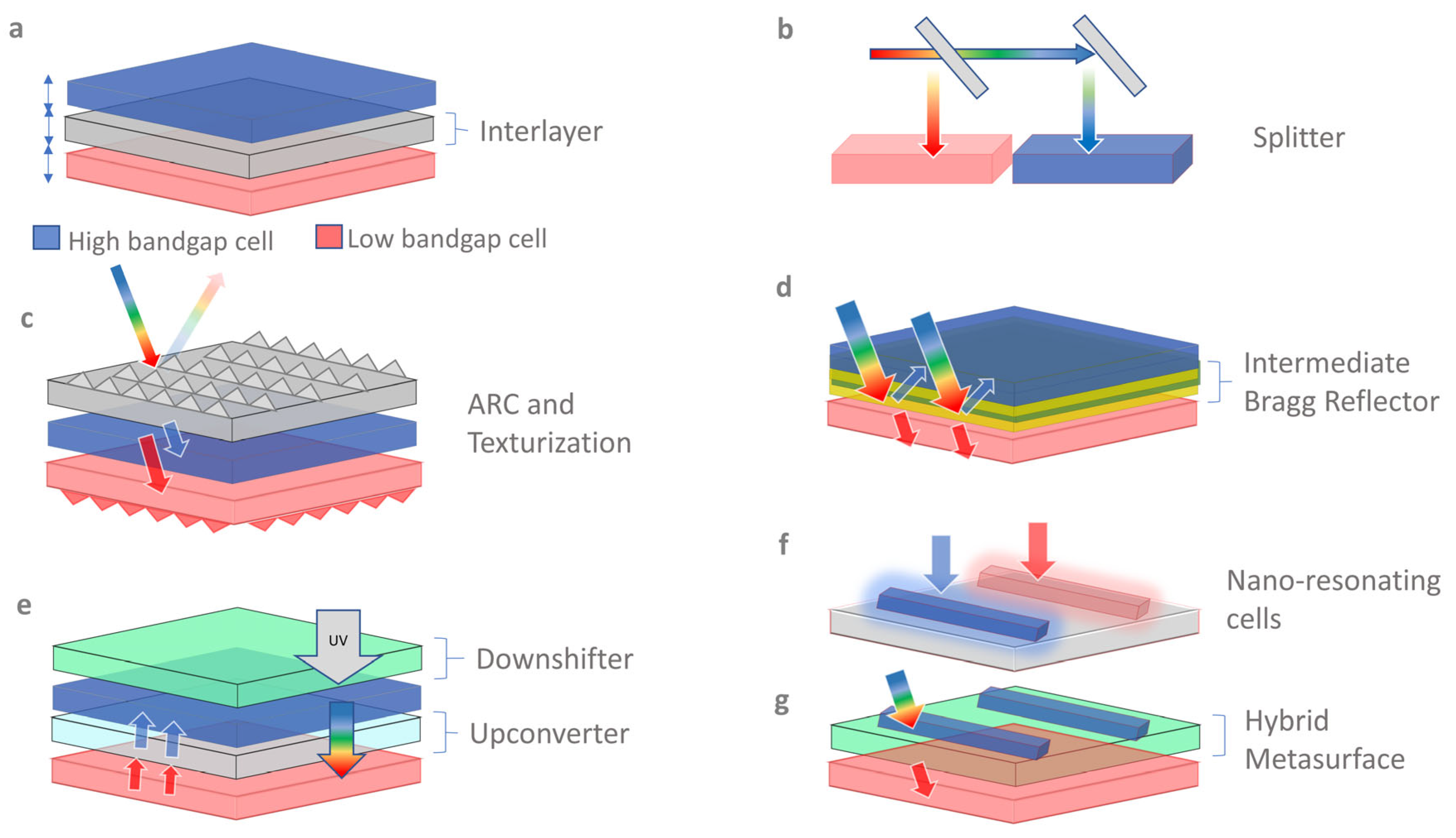
6.1.1. Active Layer and Thickness Optimization
6.1.2. Optimizing Interlayers
6.1.3. Spectrum Splitter and Reflector Optimization
6.1.4. ARC and Texturization Optimization
6.1.5. Metasurface and Metamaterial Optimization
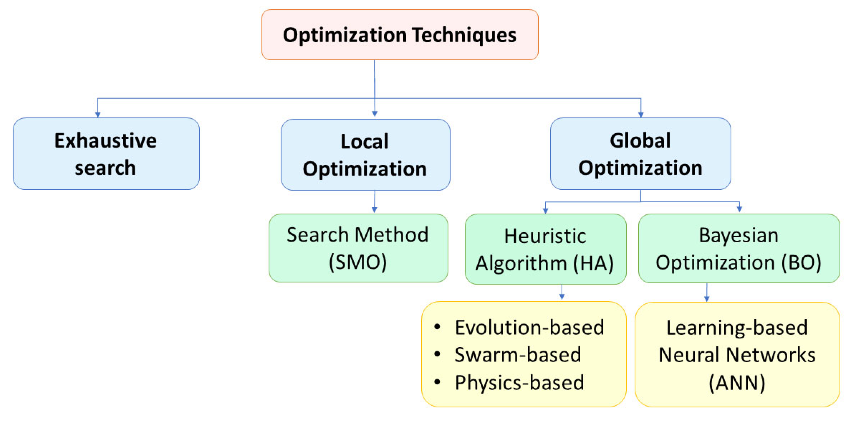
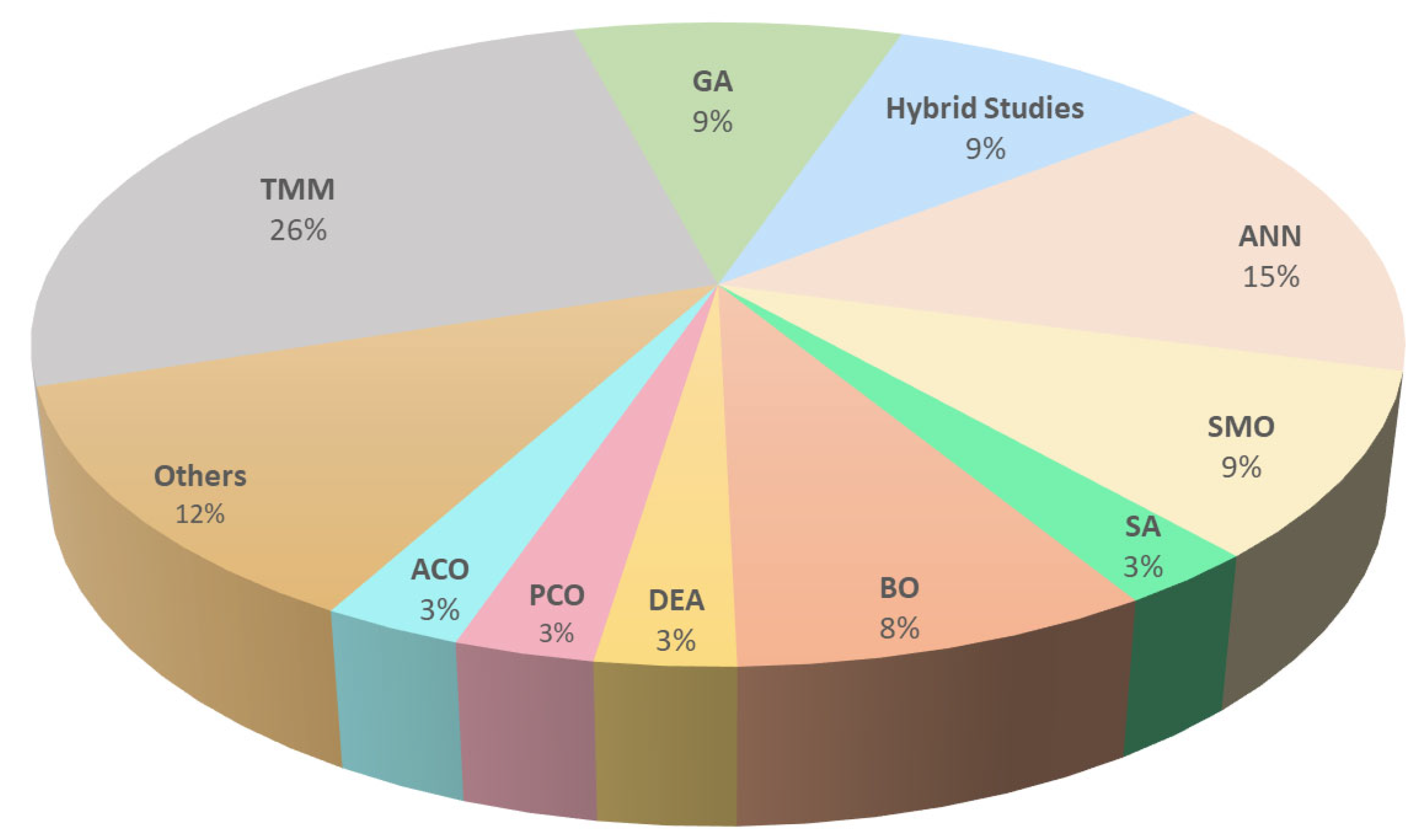
6.2. What Are Different Techniques Used for Searching for an Optimum Optical Design for TSCs in the Literature? (RQ2)
6.2.1. Exhaustive Search
6.2.2. Local Optimization (SMO)
6.2.3. Heuristic Algorithms (HAs)
6.2.4. Learning-Based Optimization
6.3. What Are the Current Learning-Based Optimization Techniques Used in the Optical Design of TSCs? (RQ3)
6.4. What Are the Key Challenges of Optical Designs and Their Optimization? (RQ4)
7. Research Gaps
8. Conclusions
Author Contributions
Funding
Data Availability Statement
Conflicts of Interest
References
- Yoshikawa, K.; Kawasaki, H.; Yoshida, W.; Irie, T.; Konishi, K.; Nakano, K.; Uto, T.; Adachi, D.; Kanematsu, M.; Uzu, H.; et al. Silicon Heterojunction Solar Cell with Interdigitated Back Contacts for a Photoconversion Efficiency over 26%. NatEn 2017, 2, 17032. [Google Scholar] [CrossRef]
- Polman, A.; Knight, M.; Garnett, E.C.; Ehrler, B.; Sinke, W.C. Photovoltaic Materials: Present Efficiencies and Future Challenges. Science 2016, 352, aad4424. [Google Scholar] [CrossRef]
- Li, K.; Zhang, S.; Ruan, Y.; Li, D.; Zhang, T.; Zhen, H. Optimization of Light Management Layers for Light Harvest of Perovskite Solar Cells. Opt. Express 2019, 27, A1004. [Google Scholar] [CrossRef]
- Elshorbagy, M.H.; López-Fraguas, E.; Chaudhry, F.A.; Sánchez-Pena, J.M.; Vergaz, R.; García-Cámara, B. A Monolithic Nanostructured-Perovskite/Silicon Tandem Solar Cell: Feasibility of Light Management through Geometry and Materials Selection. Sci. Rep. 2020, 10, 2271. [Google Scholar] [CrossRef]
- Elshorbagy, M.H.; García-Cámara, B.; López-Fraguas, E.; Vergaz, R. Efficient Light Management in a Monolithic Tandem Perovskite/Silicon Solar Cell by Using a Hybrid Metasurface. Nanomaterials 2019, 9, 791. [Google Scholar] [CrossRef] [PubMed]
- Jacobs, D.A.; Langenhorst, M.; Sahli, F.; Richards, B.S.; White, T.P.; Ballif, C.; Catchpole, K.R.; Paetzold, U.W. Light Management: A Key Concept in High-Efficiency Perovskite/Silicon Tandem Photovoltaics. J. Phys. Chem. Lett. 2019, 10, 3159–3170. [Google Scholar] [CrossRef] [PubMed]
- Ferhati, H.; Djeffal, F.; Drissi, B.L. Performance Improvement of Perovskite/CZTS Tandem Solar Cell Using Low-Cost ZnS/Ag/ITO Multilayer Spectrum Splitter. Superlattices Microstruct. 2020, 148, 106727. [Google Scholar] [CrossRef]
- Chen, D.; Manley, P. Nanophotonic Light Management for Perovskite–Silicon Tandem Solar Cells. J. Photonics Energy 2018, 8, 22601. [Google Scholar] [CrossRef]
- Hossain, M.I.; Yumnam, N.; Qarony, W.; Salleo, A.; Wagner, V.; Knipp, D.; Tsang, Y.H. Non-Resonant Metal-Oxide Metasurfaces for Efficient Perovskite Solar Cells. Sol. Energy 2020, 198, 570–577. [Google Scholar] [CrossRef]
- Subhan, F.E.; Khan, A.D.; Khan, A.D.; Ullah, N.; Imran, M.; Noman, M. Optical Optimization of Double-Side-Textured Monolithic Perovskite-Silicon Tandem Solar Cells for Improved Light Management. RSC Adv. 2020, 10, 26631–26638. [Google Scholar] [CrossRef]
- Hossain, J.; Mondal, B.K.; Mostaque, S.K.; Al Ahmed, S.R.; Shirai, H. Optimization of Multilayer Anti-Reflection Coatings for Efficient Light Management of PEDOT:PSS/c-Si Heterojunction Solar Cells. Mater. Res. Express 2019, 7, 15502. [Google Scholar] [CrossRef]
- Guo, X.; Liu, Q.; Tian, H.; Li, B.; Zhou, H.; Li, C.; Hu, A.; He, X. Optimization of Broadband Omnidirectional Antireflection Coatings for Solar Cells. J. Semicond. 2019, 40, 32702. [Google Scholar] [CrossRef]
- Sayed, H.; Matar, Z.S.; Al-Dossari, M.; Amin, A.F.; Abd El-Gawaad, N.S.; Aly, A.H. The Design and Optimization of an Anti-Reflection Coating and an Intermediate Reflective Layer to Enhance Tandem Solar Cell Photons Capture. Crystals 2022, 12, 57. [Google Scholar] [CrossRef]
- Diop, M.M.; Diaw, A.; Mbengue, N.; Ba, O.; Diagne, M.; Niasse, O.A.; Ba, B.; Sarr, J. Optimization and Modeling of Antireflective Layers for Silicon Solar Cells: In Search of Optimal Materials. Mater. Sci. Appl. 2018, 9, 705–722. [Google Scholar] [CrossRef]
- Saylan, S.; Milakovich, T.; Hadi, S.A.; Nayfeh, A.; Fitzgerald, E.A.; Dahlem, M.S. Multilayer Antireflection Coating Design for GaAs0.69P0.31/Si Dual-Junction Solar Cells. Sol. Energy 2015, 122, 76–86. [Google Scholar] [CrossRef]
- Tiguntseva, E.; Chebykin, A.; Ishteev, A.; Haroldson, R.; Balachandran, B.; Ushakova, E.; Komissarenko, F.; Wang, H.; Milichko, V.; Tsypkin, A.; et al. Resonant Silicon Nanoparticles for Enhancement of Light Absorption and Photoluminescence from Hybrid Perovskite Films and Metasurfaces. Nanoscale 2017, 9, 12486–12493. [Google Scholar] [CrossRef] [PubMed]
- Mellor, A.; Hylton, N.P.; Maier, S.A.; Ekins-Daukes, N. Interstitial Light-Trapping Design for Multi-Junction Solar Cells. Sol. Energy Mater. Sol. Cells 2017, 159, 212–218. [Google Scholar] [CrossRef]
- Yu, Z.; Leilaeioun, M.; Holman, Z. Selecting Tandem Partners for Silicon Solar Cells. Nat. Energy 2016, 1, 16137. [Google Scholar] [CrossRef]
- Cho, E.-C.; Green, M.A.; Conibeer, G.; Song, D.; Cho, Y.-H.; Scardera, G.; Huang, S.; Park, S.; Hao, X.J.; Huang, Y.; et al. Silicon Quantum Dots in a Dielectric Matrix for All-Silicon Tandem Solar Cells. Adv. Optoelectron. 2007, 2007, 69578. [Google Scholar] [CrossRef]
- Cheng, Y.; Ding, L. Perovskite/Si Tandem Solar Cells: Fundamentals, Advances, Challenges, and Novel Applications. SusMat 2021, 1, 324–344. [Google Scholar] [CrossRef]
- Martinho, F. Challenges for the Future of Tandem Photovoltaics on the Path to Terawatt Levels: A Technology Review. Energy Environ. Sci. 2021, 14, 3840–3871. [Google Scholar] [CrossRef]
- Li, B. Improved GaAsP Solar Cells with Distributed Bragg Reflector for Space Applications; Department of Electrical and Computer Engineering, University of Illinois at Urbana-Champaign: Urbana, IL, USA, 2020; pp. 1–15. [Google Scholar]
- Essig, S.; Allebé, C.; Remo, T.; Geisz, J.F.; Steiner, M.A.; Horowitz, K.; Barraud, L.; Ward, J.S.; Schnabel, M.; Descoeudres, A.; et al. Raising the One-Sun Conversion Efficiency of III–V/Si Solar Cells to 32.8% for Two Junctions and 35.9% for Three Junctions. Nat. Energy 2017, 2, 17144. [Google Scholar] [CrossRef]
- Zhang, C.; Li, X.; Shang, A.; Zhan, Y.; Yang, Z.; Wu, S. Performance-Improved Thin-Film a-Si:H/Μc-Si:H Tandem Solar Cells by Two-Dimensionally Nanopatterning Photoactive Layer. Nanoscale Res. Lett. 2014, 9, 73. [Google Scholar] [CrossRef]
- Muminov, K.K.; Mirkamali, A.S. Simulation of the Efficiency of A-SiC: H/a-Si: H Tandem Multilayer Solar Cells. arXiv 2016, arXiv:1601.06112. [Google Scholar]
- Rohatgi, A.; Zhu, K.; Tong, J.; Kim, D.H.; Reichmanis, E.; Rounsaville, B.; Prakash, V. Tandem Solar Cell Composed of a High-Performance Semitransparent Perovskite Cell and a Doped Poly-Si/SiOx Passivating Contact Silicon Cell. IEEE J. Photovolt. 2019, 10, 417–422. [Google Scholar] [CrossRef]
- Yousfi, A.; Bencherif, H.; Dehimi, L.; Pezzimenti, F.; Saidi, L.; Abdi, M.A.; Meddour, F.; Khezzar, D. Possible Efficiency Boosting of Tandem Solar Cell by Using Single Antireflection Coating and BSF Layer. In Proceedings of the 2019 1st International Conference on Sustainable Renewable Energy Systems and Applications (ICSRESA 2019), Tebessa, Algeria, 4–5 December 2019; pp. 8–11. [Google Scholar] [CrossRef]
- Boudaoud, C.; Hamdoune, A.; Allam, Z. Simulation and Optimization of a Tandem Solar Cell Based on InGaN. Math. Comput. Simul. 2020, 167, 194–201. [Google Scholar] [CrossRef]
- Even, J.; Pedesseau, L.; Tea, E.; Almosni, S.; Rolland, A.; Robert, C.; Jancu, J.-M.; Cornet, C.; Katan, C.; Guillemoles, J.-F.; et al. Density Functional Theory Simulations of Semiconductors for Photovoltaic Applications: Hybrid Organic-Inorganic Perovskites and III/V Heterostructures. Int. J. Photoenergy 2014, 2014, 649408. [Google Scholar] [CrossRef]
- Jiang, Z.; Gholamkhass, B.; Servati, P. Effects of Interlayer Properties on the Performance of Tandem Organic Solar Cells with Low and High Band Gap Polymers. J. Mater. Res. 2019, 34, 2407–2415. [Google Scholar] [CrossRef]
- Wei, F.; Yao, L.; Lan, F.; Li, G.; Liu, L. Tandem Polymer Solar Cells: Simulation and Optimization through a Multiscale Scheme. Beilstein J. Nanotechnol. 2017, 8, 123–133. [Google Scholar] [CrossRef] [PubMed]
- Abderrezek, M.; Fathi, M.; Djahli, F.; Ayad, M. Numerical Simulation of Luminescent Downshifting in Top Cell of Monolithic Tandem Solar Cells. Int. J. Photoenergy 2013, 2013, 480634. [Google Scholar] [CrossRef]
- Shi, D.; Zeng, Y.; Shen, W. Perovskite/c-Si Tandem Solar Cell with Inverted Nanopyramids: Realizing High Efficiency by Controllable Light Trapping. Sci. Rep. 2015, 5, 16504. [Google Scholar] [CrossRef]
- Mazzarella, L.; Lin, Y.H.; Kirner, S.; Morales-Vilches, A.B.; Korte, L.; Albrecht, S.; Crossland, E.; Stannowski, B.; Case, C.; Snaith, H.J.; et al. Infrared Light Management Using a Nanocrystalline Silicon Oxide Interlayer in Monolithic Perovskite/Silicon Heterojunction Tandem Solar Cells with Efficiency above 25%. Adv. Energy Mater. 2019, 9, 1803241. [Google Scholar] [CrossRef]
- Manzoor, S.; Yu, Z.; Ali, A.; Ali, W.; Bush, K.; Palmstrom, A.; Bent, S.; Mcgehee, M.; Holman, Z. Improved Light Management in Planar Silicon and Perovskite Solar Cells Using PDMS Scattering Layer. Sol. Energy Mater. Sol. Cells 2017, 173, 59–65. [Google Scholar] [CrossRef]
- Islam, M.; Wahid, S.; Alam, M.K. Physics-Based Modeling and Performance Analysis of Dual Junction Perovskite/Silicon Tandem Solar Cells. Phys. Status Solidi Appl. Mater. Sci. 2017, 214, 1600306. [Google Scholar] [CrossRef]
- Jäger, K.; Korte, L.; Rech, B.; Albrecht, S. Numerical Optical Optimization of Monolithic Planar Perovskite-Silicon Tandem Solar Cells with Regular and Inverted Device Architectures. Opt. Express 2017, 25, A473. [Google Scholar] [CrossRef]
- Green, M.A.; Emery, K.; Hishikawa, Y.; Warta, W.; Dunlop, E.D.; Levi, D.H.; Ho-Baillie, A.W.Y. Solar Cell Efficiency Tables (Version 49). Prog. Photovolt. Res. Appl. 2016, 25, 333–334. [Google Scholar] [CrossRef]
- Kayes, B.; Zhang, L.; Twist, R.; Ding, I.-K.; Higashi, G. Flexible Thin-Film Tandem Solar Cells With >30% Efficiency. Photovolt. IEEE J. 2014, 4, 729–733. [Google Scholar] [CrossRef]
- National Renewable Energy Laboratory, Best Research Cell Efficiency Chart. 2022. Available online: https://www.nrel.gov/pv/cell-efficiency.html (accessed on 18 May 2022).
- Green, M.A.; Hishikawa, Y.; Dunlop, E.D.; Levi, D.H.; Hohl-Ebinger, J.; Ho-Baillie, A.W.Y. Solar Cell Efficiency Tables (Version 51). Prog. Photovolt. Res. Appl. 2018, 26, 3–12. [Google Scholar] [CrossRef]
- Nogay, G.; Sahli, F.; Werner, J.; Monnard, R.; Boccard, M.; Despeisse, M.; Haug, F.-J.; Jeangros, Q.; Ingenito, A.; Ballif, C. 25.1%-Efficient Monolithic Perovskite/Silicon Tandem Solar Cell Based on a p-Type Monocrystalline Textured Silicon Wafer and High-Temperature Passivating Contacts. ACS Energy Lett. 2019, 4, 844–845. [Google Scholar] [CrossRef]
- Green, M.A.; Dunlop, E.D.; Levi, D.H.; Hohl-Ebinger, J.; Yoshita, M.; Ho-Baillie, A.W.Y. Solar Cell Efficiency Tables (Version 54). Prog. Photovolt. Res. Appl. 2019, 27, 565–575. [Google Scholar] [CrossRef]
- Chen, B.; Ren, N.; Li, Y.; Yan, L.; Mazumdar, S.; Zhao, Y.; Zhang, X. Insights into the Development of Monolithic Perovskite/Silicon Tandem Solar Cells. Adv. Energy Mater. 2022, 12, 2003628. [Google Scholar] [CrossRef]
- Löper, P.; Moon, S.-J.; Nicolas, S.; Niesen, B.; Ledinský, M.; Nicolay, S.; Bailat, J.; Yum, J.-H.; De Wolf, S.; Ballif, C. Organic-Inorganic Halide Perovskite/Crystalline Silicon Four-Terminal Tandem Solar Cells. Phys. Chem. Chem. Phys. 2014, 17, 1619–1629. [Google Scholar] [CrossRef]
- Mailoa, J.P.; Bailie, C.D.; Johlin, E.C.; Hoke, E.T.; Akey, A.J.; Nguyen, W.H.; McGehee, M.D.; Buonassisi, T. A 2-Terminal Perovskite/Silicon Multijunction Solar Cell Enabled by a Silicon Tunnel Junction. Appl. Phys. Lett. 2015, 106, 121105. [Google Scholar] [CrossRef]
- Almogbil, A.; Alghofaili, A.; Deane, C.; Leschke, T.; Almogbil, A.; Alghofaili, A. Digital Forensic Analysis of Fitbit Wearable Technology: An Investigator’s Guide. In Proceedings of the 2020 7th IEEE International Conference on Cyber Security and Cloud Computing (CSCloud)/2020 6th IEEE International Conference on Edge Computing and Scalable Cloud (EdgeCom), New York, NY, USA, 1–3 August 2020; pp. 44–49. [Google Scholar] [CrossRef]
- Raza, E.; Ahmad, Z. Review on Two-Terminal and Four-Terminal Crystalline-Silicon/Perovskite Tandem Solar Cells; Progress, Challenges, and Future Perspectives. Energy Rep. 2022, 8, 5820–5851. [Google Scholar] [CrossRef]
- Werner, J.; Niesen, B.; Ballif, C. Perovskite/Silicon Tandem Solar Cells: Marriage of Convenience or True Love Story?—An Overview. Adv. Mater. Interfaces 2018, 5, 1700731. [Google Scholar] [CrossRef]
- Jaysankar, M.; Qiu, W.; Van Eerden, M.; Aernouts, T.; Gehlhaar, R.; Debucquoy, M.; Paetzold, U.; Poortmans, J. Four-Terminal Perovskite/Silicon Multijunction Solar Modules. Adv. Energy Mater. 2017, 7, 1602807. [Google Scholar] [CrossRef]
- Bailie, C.D.; Christoforo, M.G.; Mailoa, J.P.; Bowring, A.R.; Unger, E.L.; Nguyen, W.H.; Burschka, J.; Pellet, N.; Lee, J.Z.; Grätzel, M.; et al. Semi-Transparent Perovskite Solar Cells for Tandems with Silicon and CIGS. Energy Environ. Sci. 2015, 8, 956–963. [Google Scholar] [CrossRef]
- Werner, J.; Dubuis, G.; Walter, A.; Löper, P.; Moon, S.-J.; Nicolay, S.; Morales-Masis, M.; De Wolf, S.; Niesen, B.; Ballif, C. Sputtered Rear Electrode with Broadband Transparency for Perovskite Solar Cells. Sol. Energy Mater. Sol. Cells 2015, 141, 407–413. [Google Scholar] [CrossRef]
- Duong, T.; Lal, N.; Grant, D.; Jacobs, D.; Zheng, P.; Rahman, S.; Shen, H.; Stocks, M.; Blakers, A.; Weber, K.; et al. Semitransparent Perovskite Solar Cell with Sputtered Front and Rear Electrodes for a Four-Terminal Tandem. IEEE J. Photovolt. 2016, 6, 679–687. [Google Scholar] [CrossRef]
- Peng, J.; Duong, T.; Zhou, X.; Shen, H.; Wu, Y.; Mulmudi, H.K.; Wan, Y.; Zhong, D.; Li, J.; Tsuzuki, T.; et al. Efficient Indium-Doped TiOx Electron Transport Layers for High-Performance Perovskite Solar Cells and Perovskite-Silicon Tandems. Adv. Energy Mater. 2017, 7, 1601768. [Google Scholar] [CrossRef]
- Zhang, D.; Najafi, M.; Zardetto, V.; Dörenkämper, M.; Zhou, X.; Veenstra, S.; Geerligs, L.J.; Aernouts, T.; Andriessen, R. High Efficiency 4-Terminal Perovskite/c-Si Tandem Cells. Sol. Energy Mater. Sol. Cells 2018, 188, 1–5. [Google Scholar] [CrossRef]
- Kanda, H.; Shibayama, N.; Uzum, A.; Umeyama, T.; Imahori, H.; Ibi, K.; Ito, S. Effect of Silicon Surface for Perovskite/Silicon Tandem Solar Cells: Flat or Textured? ACS Appl. Mater. Interfaces 2018, 10, 35016–35024. [Google Scholar] [CrossRef]
- Dewi, H.A.; Wang, H.; Li, J.; Thway, M.; Sridharan, R.; Stangl, R.; Lin, F.; Aberle, A.G.; Mathews, N.; Bruno, A.; et al. Highly Efficient Semitransparent Perovskite Solar Cells for Four Terminal Perovskite-Silicon Tandems. ACS Appl. Mater. Interfaces 2019, 11, 34178–34187. [Google Scholar] [CrossRef] [PubMed]
- Duong, T.; Pham, H.; Kho, T.C.; Phang, P.; Fong, K.C.; Yan, D.; Yin, Y.; Peng, J.; Mahmud, M.A.; Gharibzadeh, S.; et al. High Efficiency Perovskite-Silicon Tandem Solar Cells: Effect of Surface Coating versus Bulk Incorporation of 2D Perovskite. Adv. Energy Mater. 2020, 10, 1903553. [Google Scholar] [CrossRef]
- Gharibzadeh, S.; Hossain, I.M.; Fassl, P.; Nejand, B.A.; Abzieher, T.; Schultes, M.; Ahlswede, E.; Jackson, P.; Powalla, M.; Schäfer, S.; et al. 2D/3D Heterostructure for Semitransparent Perovskite Solar Cells with Engineered Bandgap Enables Efficiencies Exceeding 25% in Four-Terminal Tandems with Silicon and CIGS. Adv. Funct. Mater. 2020, 30, 1909919. [Google Scholar] [CrossRef]
- Yang, D.; Zhang, X.; Hou, Y.; Wang, K.; Ye, T.; Yoon, J.; Wu, C.; Sanghadasa, M.; Liu, S.; Priya, S. 28.3%-Efficiency Perovskite/Silicon Tandem Solar Cell by Optimal Transparent Electrode for High Efficient Semitransparent Top Cell. Nano Energy 2021, 84, 105934. [Google Scholar] [CrossRef]
- Grant, D.; Catchpole, K.; Weber, K.; White, T. Design Guidelines for Perovskite/Silicon 2-Terminal Tandem Solar Cells: An Optical Study. Opt. Express 2016, 24, A1454–A1470. [Google Scholar] [CrossRef]
- Jiang, Y.; Almansouri, I.; Huang, S.; Young, T.; Li, Y.; Peng, Y.; Hou, Q.; Spiccia, L.; Bach, U.; Cheng, Y.B.; et al. Optical Analysis of Perovskite/Silicon Tandem Solar Cells. J. Mater. Chem. C 2016, 4, 5679–5689. [Google Scholar] [CrossRef]
- Sahli, F.; Kamino, B.A.; Werner, J.; Bräuninger, M.; Paviet-Salomon, B.; Barraud, L.; Monnard, R.; Seif, J.P.; Tomasi, A.; Jeangros, Q.; et al. Improved Optics in Monolithic Perovskite/Silicon Tandem Solar Cells with a Nanocrystalline Silicon Recombination Junction. Adv. Energy Mater. 2018, 8, 1701609. [Google Scholar] [CrossRef]
- Sahli, F.; Werner, J.; Kamino, B.A.; Bräuninger, M.; Monnard, R.; Paviet-Salomon, B.; Barraud, L.; Ding, L.; Diaz Leon, J.J.; Sacchetto, D.; et al. Fully Textured Monolithic Perovskite/Silicon Tandem Solar Cells with 25.2% Power Conversion Efficiency. Nat. Mater. 2018, 17, 820–826. [Google Scholar] [CrossRef]
- Mazzarella, L.; Werth, M.; Jäger, K.; Jošt, M.; Korte, L.; Albrecht, S.; Schlatmann, R.; Stannowski, B. Infrared Photocurrent Management in Monolithic Perovskite/Silicon Heterojunction Tandem Solar Cells by Using a Nanocrystalline Silicon Oxide Interlayer. Opt. Express 2018, 26, A487–A497. [Google Scholar] [CrossRef]
- Elshorbagy, M.H.; Abdelhady, K.; Kamal, H.; Alda, J. Broadband Anti-Reflection Coating Using Dielectric Si3N4 Nanostructures. Application to Amorphous-Si-H Solar Cells. Opt. Commun. 2017, 390, 130–136. [Google Scholar] [CrossRef]
- Yang, J.; You, J.; Chen, C.C.; Hsu, W.C.; Tan, H.R.; Zhang, X.W.; Hong, Z.; Yang, Y. Plasmonic Polymer Tandem Solar Cell. ACS Nano 2011, 5, 6210–6217. [Google Scholar] [CrossRef]
- Lemercier, T.; Perrin, L.; Planès, E.; Berson, S.; Flandin, L. A Comparison of the Structure and Properties of Opaque and Semi-Transparent NIP/PIN-Type Scalable Perovskite Solar Cells. Energies 2020, 13, 3794. [Google Scholar] [CrossRef]
- Hamza, B.; Abdelkader, B.; Meskine, S.; Hadjab, M.; Ziane, M.; Zaoui, A. First Principles Investigation of Optoelectronic Properties of ZnXP2 (X = Si, Ge) Lattice Matched with Silicon for Tandem Solar Cells Applications Using the MBJ Exchange Potential. Opt.—Int. J. Light Electron Opt. 2018, 159, 229–244. [Google Scholar] [CrossRef]
- Jong, U.-G.; Yu, C.-J.; Kye, Y.-H.; Choe, Y.-G.; Hao, W.; Li, S. First-Principles Study on Structural, Electronic, and Optical Properties of Inorganic Ge-Based Halide Perovskites. Inorg. Chem. 2019, 58, 4134–4140. [Google Scholar] [CrossRef] [PubMed]
- Neupane, U.; Bahrami, B.; Biesecker, M.; Baroughi, M.F.; Qiao, Q. Kinetic Monte Carlo Modeling on Organic Solar Cells: Domain Size, Donor-Acceptor Ratio and Thickness. Nano Energy 2017, 35, 128–137. [Google Scholar] [CrossRef]
- Mousa, M.; Amer, F.Z.; Mubarak, R.I.; Saeed, A. Simulation of Optimized High-Current Tandem Solar-Cells with Efficiency beyond 41%. IEEE Access 2021, 9, 49724–49737. [Google Scholar] [CrossRef]
- Albrecht, S.; Saliba, M.; Correa-Baena, J.-P.; Jäger, K.; Korte, L.; Hagfeldt, A.; Graetzel, M.; Rech, B. Towards Optical Optimization of Planar Monolithic Perovskite/Silicon-Heterojunction Tandem Solar Cells. J. Opt. 2016, 18, 64012. [Google Scholar] [CrossRef]
- Tan, H.Q.; Zhao, X.; Jiao, A.; Birgersson, E.; Xue, H. Optimizing Bifacial All-Perovskite Tandem Solar Cell: How to Balance Light Absorption and Recombination. Sol. Energy 2022, 231, 1092–1106. [Google Scholar] [CrossRef]
- Cherif, F.E.; Sammouda, H. Optoelectronic Simulation and Optimization of Tandem and Multi-Junction Perovskite Solar Cells Using Concentrating Photovoltaic Systems. Energy Rep. 2021, 7, 5895–5908. [Google Scholar] [CrossRef]
- Rabady, R.I.; Manasreh, H. Thicknesses Optimization of Two- and Three-Junction Photovoltaic Cells with Matched Currents and Matched Lattice Constants. Sol. Energy 2017, 158, 20–27. [Google Scholar] [CrossRef]
- Yi, C.; Wu, Y.; Gao, Y.; Du, Q. Tandem Solar Cells Efficiency Prediction and Optimizationviadeep Learning. Phys. Chem. Chem. Phys. 2021, 23, 2991–2998. [Google Scholar] [CrossRef]
- Aman, G.; Jahangir, K.; Usman, Y.; Saleem, M.; Khalid, M. Numerical Modeling and Optimization of Perovskite Silicon Tandem Solar Cell Using SCAPS-1D. Sch. Bull. 2021, 7, 171–184. [Google Scholar] [CrossRef]
- Chaudhary, J.K.; Liu, J.; Skön, J.P.; Chen, Y.W.; Kanth, R.K.; Heikkonen, J. Optimization of Silicon Tandem Solar Cells Using Artificial Neural Networks; Springer International Publishing: Berlin/Heidelberg, Germany, 2019; Volume 11927, ISBN 9783030348847. [Google Scholar]
- Saidi, W.A.; Shadid, W.; Castelli, I.E. Machine-Learning Structural and Electronic Properties of Metal Halide Perovskites Using a Hierarchical Convolutional Neural Network. NPJ Comput. Mater. 2020, 6, 36. [Google Scholar] [CrossRef]
- Manuela, H. Optimization Algorithms for Improving the Effciency of a Tandem Solar Cell. Bachelor’s Thesis, Delft University, Delft, The Netherlands, 2020. [Google Scholar]
- Aeberhard, U.; Schiller, A.; Masson, Y.; Zeder, S.J.; Blülle, B.; Ruhstaller, B. Analysis and Optimization of Organic Tandem Solar Cells by Full Opto-Electronic Simulation. Front. Photonics 2022, 3, 891565. [Google Scholar] [CrossRef]
- Raghvendra; Kumar, R.R.; Pandey, S.K. Device Modeling and Optimization for an Efficient Two-Terminal Perovskite Tandem Solar Cell. J. Electron. Mater. 2022, 51, 6603–6613. [Google Scholar] [CrossRef]
- Tockhorn, P.; Sutter, J.; Cruz, A.; Wagner, P.; Jäger, K.; Yoo, D.; Lang, F.; Grischek, M.; Li, B.; Li, J.; et al. Nano-Optical Designs for High-Efficiency Monolithic Perovskite–Silicon Tandem Solar Cells. Nat. Nanotechnol. 2022, 17, 1214–1221. [Google Scholar] [CrossRef]
- Gulomov, J.; Accouche, O.; Aliev, R.; Neji, B.; Ghandour, R.; Gulomova, I.; Azab, M. Geometric Optimization of Perovskite Solar Cells with Metal Oxide Charge Transport Layers. Nanomaterials 2022, 12, 2692. [Google Scholar] [CrossRef] [PubMed]
- Xie, Y.-M.; Yao, Q.; Zeng, Z.; Xue, Q.; Niu, T.; Xia, R.; Cheng, Y.; Lin, F.; Tsang, S.-W.; Jen, A.K.-Y.; et al. Homogeneous Grain Boundary Passivation in Wide-Bandgap Perovskite Films Enables Fabrication of Monolithic Perovskite/Organic Tandem Solar Cells with over 21% Efficiency. Adv. Funct. Mater. 2022, 32, 2112126. [Google Scholar] [CrossRef]
- Kanda, H.; Dan Mihailetchi, V.; Gueunier-Farret, M.-E.; Kleider, J.-P.; Djebbour, Z.; Alvarez, J.; Philippe, B.; Isabella, O.; Vogt, M.R.; Santbergen, R.; et al. Three-Terminal Perovskite/Integrated Back Contact Silicon Tandem Solar Cells under Low Light Intensity Conditions. Interdiscip. Mater. 2022, 1, 148–156. [Google Scholar] [CrossRef]
- Yang, G.; Ni, Z.; Yu, Z.J.; Larson, B.W.; Yu, Z.; Chen, B.; Alasfour, A.; Xiao, X.; Luther, J.M.; Holman, Z.C.; et al. Defect Engineering in Wide-Bandgap Perovskites for Efficient Perovskite–Silicon Tandem Solar Cells. Nat. Photonics 2022, 16, 588–594. [Google Scholar] [CrossRef]
- Salah, M.M.; Zekry, A.; Shaker, A.; Abouelatta, M.; Mousa, M.; Saeed, A. Investigation of Electron Transport Material-Free Perovskite/CIGS Tandem Solar Cell. Energies 2022, 15, 6326. [Google Scholar] [CrossRef]
- Jaysankar, M.; Filipič, M.; Zielinski, B.; Schmager, R.; Song, W.; Qiu, W.; Paetzold, U.W.; Aernouts, T.; Debucquoy, M.; Gehlhaar, R.; et al. Perovskite-Silicon Tandem Solar Modules with Optimised Light Harvesting. Energy Environ. Sci. 2018, 11, 1489–1498. [Google Scholar] [CrossRef]
- Hajjiah, A.; Parmouneh, F.; Hadipour, A.; Jaysankar, M.; Aernouts, T. Light Management Enhancement for Four-Terminal Perovskite-Silicon Tandem Solar Cells: The Impact of the Optical Properties and Thickness of the Spacer Layer between Sub-Cells. Mater. 2018, 11, 2570. [Google Scholar] [CrossRef] [PubMed]
- Purkayastha, A.; Mallajosyula, A.T. Effect of Various Interlayers on the Performance of Cesium Formamidinium Lead Mixed Halide (CsFAPbX3)—Formamidinium Tin Iodide (FASnI3) Two-Terminal Tandem Solar Cell. Sol. Energy 2021, 228, 523–530. [Google Scholar] [CrossRef]
- Wang, Z.; Zhu, X.; Zuo, S.; Chen, M.; Zhang, C.; Wang, C.; Ren, X.; Yang, Z.; Liu, Z.; Xu, X.; et al. 27%-Efficiency Four-Terminal Perovskite/Silicon Tandem Solar Cells by Sandwiched Gold Nanomesh. Adv. Funct. Mater. 2020, 30, 1908298. [Google Scholar] [CrossRef]
- Chen, J.-T.; Hsu, C.-S. Conjugated Polymer Nanostructures for Organic Solar Cell Applications. Polym. Chem. 2011, 2, 2707–2722. [Google Scholar] [CrossRef]
- Bakour, A.; Saadoune, A.; Bouchama, I.; Dhiabi, F.; Boudour, S.; Saeed, M.A. Effect and Optimization of ZnO Layer on the Performance of GaInP/GaAs Tandem Solar Cell. Micro Nanostruct. 2022, 168, 207294. [Google Scholar] [CrossRef]
- Liu, X.; Huang, Q.; Yang, X.; Zhou, J.; Ren, C.; Su, X.; Xu, Z.; Zhao, Y.; Hou, G. Simulation of P-Type c-Si Solar Cells with Metal Oxides as Carrier-Selective Contacts. Sol. Energy 2022, 240, 84–89. [Google Scholar] [CrossRef]
- Werner, J. Perovskite/Silicon Tandem Solar Cells: Toward Affordable Ultra-High Efficiency Photovoltaics? EPFL: Lausanne, Switzerland, 2018; Volume 8659, pp. 1–161. [Google Scholar]
- Üpping, J.; Bielawny, A.; Wehrspohn, R.B.; Beckers, T.; Carius, R.; Rau, U.; Fahr, S.; Rockstuhl, C.; Lederer, F.; Kroll, M.; et al. Three-Dimensional Photonic Crystal Intermediate Reflectors for Enhanced Light-Trapping in Tandem Solar Cells. Adv. Mater. 2011, 23, 3896–3900. [Google Scholar] [CrossRef]
- Yadav, C.; Kumar, S. Numerical Simulation of Novel Designed Perovskite/Silicon Heterojunction Solar Cell. Opt. Mater. 2022, 123, 111847. [Google Scholar] [CrossRef]
- Hossain, I.M.; Donie, Y.J.; Schmager, R.; Abdelkhalik, M.S.; Rienäcker, M.; Wietler, T.F.; Peibst, R.; Karabanov, A.; Schwenzer, J.A.; Moghadamzadeh, S.; et al. Nanostructured Front Electrodes for Perovskite/c-Si Tandem Photovoltaics. Opt. Express 2020, 28, 8878. [Google Scholar] [CrossRef]
- Jalali, T.; Jafari, M.; Mohammadi, A. Genetic Algorithm Optimization of Antireflection Coating Consisting of Nanostructured Thin Films to Enhance Silicon Solar Cell Efficacy. Mater. Sci. Eng. B 2019, 247, 114354. [Google Scholar] [CrossRef]
- Li, S.; Cao, Y.L.; Li, W.H.; Bo, Z.S. A Brief Review of Hole Transporting Materials Commonly Used in Perovskite Solar Cells. Rare Met. 2021, 40, 2712–2729. [Google Scholar] [CrossRef]
- Wang, Q.; Zhang, X.; Jin, Z.; Zhang, J.; Gao, Z.; Li, Y.; Liu, S.F. Energy-Down-Shift CsPbCl3:Mn Quantum Dots for Boosting the Efficiency and Stability of Perovskite Solar Cells. ACS Energy Lett. 2017, 2, 1479–1486. [Google Scholar] [CrossRef]
- Uzu, H.; Ichikawa, M.; Hino, M.; Nakano, K.; Meguro, T.; Hernandez, J.L.; Kim, H.-S.; Park, N.-G.; Yamamoto, K. High Efficiency Solar Cells Combining a Perovskite and a Silicon Heterojunction Solar Cells via an Optical Splitting System. Appl. Phys. Lett. 2015, 106, 13506. [Google Scholar] [CrossRef]
- Kumar, K.; Das, A.; Kumawat, U.K.; Dhawan, A. Enhanced Performance of Triple-Junction Tandem Organic Solar Cells Due to the Presence of Plasmonic Nanoparticles. Energy Sci. Eng. 2022, 10, 230–242. [Google Scholar] [CrossRef]
- Mann, S.A.; Garnett, E.C. Resonant Nanophotonic Spectrum Splitting for Ultrathin Multijunction Solar Cells. ACS Photonics 2015, 2, 816–821. [Google Scholar] [CrossRef]
- Van Der Burgt, J.S.; Garnett, E.C. Nanophotonic Emission Control for Improved Photovoltaic Efficiency. ACS Photonics 2020, 7, 1589–1602. [Google Scholar] [CrossRef]
- Dorodnyy, A.; Alarcon-Lladó, E.; Shklover, V.; Hafner, C.; Fontcuberta i Morral, A.; Leuthold, J. Efficient Multiterminal Spectrum Splitting via a Nanowire Array Solar Cell. ACS Photonics 2015, 2, 1284–1288. [Google Scholar] [CrossRef] [PubMed]
- Mann, S.A.; Grote, R.R.; Osgood, R.M.; Alù, A.; Garnett, E.C. Opportunities and Limitations for Nanophotonic Structures to Exceed the Shockley-Queisser Limit. ACS Nano 2016, 10, 8620–8631. [Google Scholar] [CrossRef] [PubMed]
- Li, H.; He, Y.; Wang, C.; Wang, X.; Hu, Y. Tunable Thermal and Electricity Generation Enabled by Spectrally Selective Absorption Nanoparticles for Photovoltaic/Thermal Applications. Appl. Energy 2019, 236, 117–126. [Google Scholar] [CrossRef]
- Yolalmaz, A.; Yüce, E. Spectral Splitting and Concentration of Broadband Light Using Neural Networks. APL Photonics 2021, 6, 46101. [Google Scholar] [CrossRef]
- Yu, Z.J.; Fisher, K.C.; Wheelwright, B.M.; Angel, R.P.; Holman, Z.C. PVMirror: A New Concept for Tandem Solar Cells and Hybrid Solar Converters. IEEE J. Photovolt. 2015, 5, 1791–1799. [Google Scholar] [CrossRef]
- Grant, D.T.; Weber, K.J.; Stocks, M.; White, T.P. Optical Optimization of Perovskite-Silicon Reflective Tandem Solar Cells. In Optical Nanostructures and Advanced Materials for Photovoltaics; Optica Publishing Group: Washington, DC, USA, 2015; p. PTh3B.3. [Google Scholar]
- Duong, T.; Grant, D.; Rahman, S.; Blakers, A.; Weber, K.J.; Catchpole, K.R.; White, T.P. Filterless Spectral Splitting Perovskite–Silicon Tandem System with Gt;23% Calculated Efficiency. IEEE J. Photovolt. 2016, 6, 1432–1439. [Google Scholar] [CrossRef]
- Kinoshita, T.; Nonomura, K.; Jeon, N.J.; Giordano, F.; Abate, A.; Uchida, S.; Kubo, T.; Seok, S.I.; Nazeeruddin, M.K.; Hagfeldt, A.; et al. Spectral Splitting Photovoltaics Using Perovskite and Wideband Dye-Sensitized Solar Cells. Nat. Commun. 2015, 6, 8834. [Google Scholar] [CrossRef]
- Nakamura, M.; Tada, K.; Kinoshita, T.; Bessho, T.; Nishiyama, C.; Takenaka, I.; Kimoto, Y.; Higashino, Y.; Sugimoto, H.; Segawa, H. Perovskite/CIGS Spectral Splitting Double Junction Solar Cell with 28% Power Conversion Efficiency. iScience 2020, 23, 101817. [Google Scholar] [CrossRef]
- Sheng, R.; Ho-Baillie, A.; Huang, S.; Keevers, M.; Hao, X.; Liangcong, J.; Bing, C.; Green, M. 4-Terminal Tandem Solar Cells Using CH 3 NH 3 PbBr 3 by Spectrum Splitting. J. Phys. Chem. Lett. 2015, 6, 3931–3934. [Google Scholar] [CrossRef]
- Ayala Mató, F.; Seuret-Jimenez, D.; Vigil, O.; Escobedo, J. Use of TCO as Splitter in the Optical Splitting System for Solar Cells Combination: A Simulation Study. Mater. Res. Express 2017, 4, 105503. [Google Scholar] [CrossRef]
- Ayala-Mató, F.; Seuret-Jiménez, D.; Vigil-Galán, O.; Escobedo-Alatorre, J.J.; Courel, M. Numerical Evaluation of the Optical-Splitter System Efficiency Using a TCO as Optical Splitter. Mater. Res. Express 2019, 6, 45903. [Google Scholar] [CrossRef]
- Yu, Z.J.; Fisher, K.C.; Holman, Z.C. Modeling of GaAs/Silicon PVMirror Tandem System: A Case Study. In Proceedings of the 2017 IEEE 44th Photovoltaic Specialists Conference (PVSC 2017), Washington, DC, USA, 25–30 June 2017; pp. 1430–1434. [Google Scholar] [CrossRef]
- Eisler, C.N.; Flowers, C.A.; Warmann, E.C.; Lloyd, J.V.; Espinet-Gonzalez, P.; Darbe, S.; Dee, M.S.; Escarra, M.D.; Kosten, E.D.; Zhou, W.; et al. The Polyhedral Specular Reflector: A Spectrum-Splitting Multijunction Design to Achieve Ultrahigh (>50%) Solar Module Efficiencies. IEEE J. Photovolt. 2019, 9, 174–182. [Google Scholar] [CrossRef]
- Jošt, M.; Köhnen, E.; Morales-Vilches, A.B.; Lipovšek, B.; Jäger, K.; Macco, B.; Al-Ashouri, A.; Krč, J.; Korte, L.; Rech, B.; et al. Textured Interfaces in Monolithic Perovskite/Silicon Tandem Solar Cells: Advanced Light Management for Improved Efficiency and Energy Yield. Energy Environ. Sci. 2018, 11, 3511–3523. [Google Scholar] [CrossRef]
- Liu, Z.; Ren, Z.; Liu, H.; Sahraei, N.; Lin, F.; Stangl, R.; Aberle, A.G.; Buonassisi, T.; Peters, I.M. A Modeling Framework for Optimizing Current Density in Four-Terminal Tandem Solar Cells: A Case Study on GaAs/Si Tandem. Sol. Energy Mater. Sol. Cells 2017, 170, 167–177. [Google Scholar] [CrossRef]
- Chen, B.; Baek, S.W.; Hou, Y.; Aydin, E.; De Bastiani, M.; Scheffel, B.; Proppe, A.; Huang, Z.; Wei, M.; Wang, Y.K.; et al. Enhanced Optical Path and Electron Diffusion Length Enable High-Efficiency Perovskite Tandems. Nat. Commun. 2020, 11, 1257. [Google Scholar] [CrossRef] [PubMed]
- Hadi, A.; Milakovich, T.; Bulsara, M.T.; Dahlem, M.S.; Fitzgerald, E.A.; Link, C.; Hadi, S.A.; Milakovich, T.; Bulsara, M.T.; Saylan, S.; et al. Design Optimization of Single Layer Anti—Reflective Coating for GaAs1−xPx/Si Tandem. IEEE J. Photovolt. 2018, 5, 425–431. [Google Scholar]
- Neder, V.; Zhang, D.; Veenstra, S.; Polman, A. Four-Terminal Perovskite/Silicon Tandem Solar Cell with Integrated Mie-Resonant Spectral Splitter Metagrating. arXiv 2020, arXiv:2012.12649. [Google Scholar]
- Wang, C.; Zhang, Z. Broadband Optical Absorption Enhancement in Hybrid Organic-Inorganic Perovskite Metasurfaces. AIP Adv. 2021, 11, 25107. [Google Scholar] [CrossRef]
- Bittkau, K.; Kirchartz, T.; Rau, U. Optical Design of Spectrally Selective Interlayers for Perovskite/Silicon Heterojunction Tandem Solar Cells. Opt. Express 2018, 26, A750–A760. [Google Scholar] [CrossRef]
- Martins, A.; Borges, B.-H.; Li, J.; Krauss, T.F.; Martins, E. Photonic Intermediate Structures for Perovskite/c-Silicon Four Terminal Tandem Solar Cells. IEEE J. Photovolt. 2017, 7, 1190–1196. [Google Scholar] [CrossRef]
- Jiang, Y.; Keevers, M.J.; Green, M.A. Design of Bragg Reflector in GaInP/GaInAs/Ge Triple-Junction Solar Cells for Spectrum Splitting Applications. In Proceedings of the 2018 IEEE 7th World Conference on Photovoltaic Energy Conversion (WCPEC) (A Joint Conference of 45th IEEE PVSC, 28th PVSEC & 34th EU PVSEC), Waikoloa Village, HI, USA, 10–15 June 2018. [Google Scholar]
- Jiang, Y.; Keevers, M.J.; Pearce, P.; Ekins-Daukes, N.; Green, M.A. Design of an Intermediate Bragg Reflector within Triple-Junction Solar Cells for Spectrum Splitting Applications. Sol. Energy Mater. Sol. Cells 2019, 193, 259–269. [Google Scholar] [CrossRef]
- Lepkowski, D.L.; Kasher, T.; Grassman, T.J.; Ringel, S.A. Designing an Epitaxially-Integrated DBR for Dislocation Mitigation in Monolithic GaAsP/Si Tandem Solar Cells. IEEE J. Photovolt. 2021, 11, 400–407. [Google Scholar] [CrossRef]
- Bouzid, F.; Pezzimenti, F.; Dehimi, L.; Della Corte, F.G.; Hadjab, M.; Hadj Larbi, A. Analytical Modeling of Dual-Junction Tandem Solar Cells Based on an InGaP/GaAs Heterojunction Stacked on a Ge Substrate. J. Electron. Mater. 2019, 48, 4107–4116. [Google Scholar] [CrossRef]
- France, R.M.; Espinet-Gonzalez, P.; Ekins-Daukes, N.J.; Guthrey, H.; Steiner, M.A.; Geisz, J.F. Multijunction Solar Cells with Graded Buffer Bragg Reflectors. IEEE J. Photovolt. 2018, 8, 1608–1615. [Google Scholar] [CrossRef]
- Farooq, W.; Tu, S.; Ali Kazmi, S.A.; Rehman, S.U.; Khan, A.D.; Khan, H.A.; Waqas, M.; Rehman, O.U.; Ali, H.; Noman, M. Novel Perovskite Solar Cell with Distributed Bragg Reflector. PLoS ONE 2021, 16, e0259778. [Google Scholar] [CrossRef]
- Rouhbakhshmeghrazi, A.; Madadi, M. Novel Design of Polycrystalline CdTe/Si Tandem Solar Cells Using SiO2/TiO2 Distributed Bragg Reflector. Tecciencia 2020, 15, 67–75. [Google Scholar] [CrossRef]
- Civiletti, B.J.; Anderson, T.H.; Ahmad, F.; Monk, P.B.; Lakhtakia, A. Optimization Approach for Optical Absorption in Three-Dimensional Structures Including Solar Cells. Opt. Eng. 2018, 57, 57101. [Google Scholar] [CrossRef]
- Li, Q.; Wang, S.; Zhang, M.; Feng, L.; Su, X.; Ding, W.; Li, Y.; Yun, F. ITO Nanowire Networks Coating on µ-Hole Arrayed Substrate as Super-Broadband Antireflection Layer. Sol. Energy 2018, 173, 590–596. [Google Scholar] [CrossRef]
- Sikder, U.; Zaman, M.A. Optimization of Multilayer Antireflection Coating for Photovoltaic Applications. Opt. Laser Technol. 2016, 79, 88–94. [Google Scholar] [CrossRef]
- Hamouche, H.; Shabat, M.M.; Schaadt, D.M. Multilayer Solar Cell Waveguide Structures Containing Metamaterials. Superlattices Microstruct. 2017, 101, 633–640. [Google Scholar] [CrossRef]
- Jäger, K.; Sutter, J.; Hammerschmidt, M.; Schneider, P.I.; Becker, C. Prospects of Light Management in Perovskite/Silicon Tandem Solar Cells. Nanophotonics 2021, 10, 1991–2000. [Google Scholar] [CrossRef]
- Altazin, S.; Stepanova, L.; Werner, J.; Niesen, B.; Ballif, C.; Ruhstaller, B. Design of Perovskite/Crystalline-Silicon Monolithic Tandem Solar Cells. Opt. Express 2018, 26, A579. [Google Scholar] [CrossRef] [PubMed]
- Razzaq, A.; Depauw, V.; Radhakrishnan, H.S.; Cho, J.; Gordon, I.; Szlufcik, J.; Abdulraheem, Y.; Poortmans, J. Infrared Absorption Enhancement Using Periodic Inverse Nanopyramids in Crystalline-Silicon Bottom Cells for Application in Tandem Devices. IEEE J. Photovolt. 2020, 10, 740–748. [Google Scholar] [CrossRef]
- Razzaq, A.; Mayer, A.; Depauw, V.; Gordon, I.; Hajjiah, A.; Poortmans, J. Application of a Genetic Algorithm in Four-Terminal Perovskite/Crystalline-Silicon Tandem Devices. IEEE J. Photovolt. 2020, 10, 1689–1700. [Google Scholar] [CrossRef]
- Ding, F.; Wang, Z.; He, S.; Shalaev, V.M.; Kildishev, A.V. Broadband High-Efficiency Half-Wave Plate: A Supercell-Based Plasmonic Metasurface Approach. ACS Nano 2015, 9, 4111–4119. [Google Scholar] [CrossRef]
- Aoni, R.A.; Rahmani, M.; Xu, L.; Zangeneh Kamali, K.; Komar, A.; Yan, J.; Neshev, D.; Miroshnichenko, A.E. High-Efficiency Visible Light Manipulation Using Dielectric Metasurfaces. Sci. Rep. 2019, 9, 6510. [Google Scholar] [CrossRef] [PubMed]
- Piralaee, M.; Asgari, A. The Role of Silver Nanoparticles in Performance of Multi-Quantum Well Double Heterojunction InGaN/GaN Solar Cells. Chem. Phys. Lett. 2020, 754, 137500. [Google Scholar] [CrossRef]
- Nematpour, A.; Nikoufard, M.; Changizi, S. Simulation, Design and Optimization of Si/InP Thin-Film Tandem Solar Cell by Using a Plasmonic Back Reflector Structure. Indian J. Phys. 2021, 95, 1509–1516. [Google Scholar] [CrossRef]
- Kuang, Y.; Ma, Y.; Zhang, D.; Wei, Q.; Wang, S.; Yang, X.; Hong, X.; Liu, Y. Enhanced Optical Absorption in Perovskite/Si Tandem Solar Cells with Nanoholes Array. Nanoscale Res. Lett. 2020, 15, 213. [Google Scholar] [CrossRef]
- Manley, P.; Arnaoutakis, G.; Macqueen, R.W.; Burger, S.; Becker, C. Double-Layer Metasurface for Enhanced Photon up-Conversion. AIP Adv. 2021, 6, 36103. [Google Scholar] [CrossRef]
- Zheng, J.; Mehrvarz, H.; Liao, C.; Bing, J.; Cui, X.; Li, Y.; Goncąles, V.R.; Lau, C.F.J.; Lee, D.S.; Li, Y.; et al. Large-Area 23%-Efficient Monolithic Perovskite/Homojunction-Silicon Tandem Solar Cell with Enhanced Uv Stability Using down-Shifting Material. ACS Energy Lett. 2019, 4, 2623–2631. [Google Scholar] [CrossRef]
- Meng, L.; Wu, X.-G.; Ma, S.; Shi, L.; Zhang, M.; Wang, L.; Chen, Y.; Chen, Q.; Zhong, H. Improving the Efficiency of Silicon Solar Cells Using in Situ Fabricated Perovskite Quantum Dots as Luminescence Downshifting Materials. Nanophotonics 2020, 9, 93–100. [Google Scholar] [CrossRef]
- Uleman, F.; Neder, V.; Cordaro, A.; Alù, A.; Polman, A. Resonant Metagratings for Spectral and Angular Control of Light for Colored Rooftop Photovoltaics. ACS Appl. Energy Mater. 2020, 3, 3150–3156. [Google Scholar] [CrossRef]
- Neder, V. Dielectric Metasurfaces for Light Management in Photovoltaics; Universiteit van Amsterdam: Amsterdam, The Netherlands, 2021. [Google Scholar]
- Noureen, S.; Zubair, M.; Ali, M.; Mehmood, M.Q. Deep Learning Based Hybrid Sequence Modeling for Optical Response Retrieval in Metasurfaces for STPV Applications. Opt. Mater. Express 2021, 11, 3178–3193. [Google Scholar] [CrossRef]
- Nadell, C.; Huang, B.; Malof, J.; Padilla, W. Deep Learning for Accelerated All-Dielectric Metasurface Design. Opt. Express 2019, 27, 27523. [Google Scholar] [CrossRef] [PubMed]
- An, S.; Zheng, B.; Shalaginov, M.Y.; Tang, H.; Li, H.; Zhou, L.; Ding, J.; Agarwal, A.M.; Rivero-Baleine, C.; Kang, M.; et al. Deep Learning Modeling Approach for Metasurfaces with High Degrees of Freedom. Opt. Express 2020, 28, 31932–31942. [Google Scholar] [CrossRef]
- Yeung, C.; Tsai, J.-M.; King, B.; Pham, B.; Ho, D.; Liang, J.; Knight, M.W.; Raman, A.P. Multiplexed Supercell Metasurface Design and Optimization with Tandem Residual Networks. Nanophotonics 2021, 10, 1133–1143. [Google Scholar] [CrossRef]
- Zhen, Z.; Qian, C.; Jia, Y.; Fan, Z.; Hao, R.; Cai, T.; Zheng, B.; Chen, H.; Li, E. Realizing Transmitted Metasurface Cloak by a Tandem Neural Network. Photon. Res. 2021, 9, B229–B235. [Google Scholar] [CrossRef]
- Zhu, R.; Qiu, T.; Wang, J.; Sui, S.; Hao, C.; Liu, T.; Li, Y.; Feng, M.; Zhang, A.; Qiu, C.-W.; et al. Phase-to-Pattern Inverse Design Paradigm for Fast Realization of Functional Metasurfaces via Transfer Learning. Nat. Commun. 2021, 12, 2974. [Google Scholar] [CrossRef]
- Jiang, L.; Li, X.; Wu, Q.; Wang, L.; Gao, L. Neural Network Enabled Metasurface Design for Phase Manipulation. Opt. Express 2021, 29, 2521–2528. [Google Scholar] [CrossRef]
- Soeriyadi, A.; Wang, L.; Conrad, B.; Zhao, X.; Li, D.; Lochtefeld, A.; Gerger, A.; Barnett, A.M.; Perez-Wurfl, I. Spatially Resolved EL and PL Coupling of a Dual Junction Solar Cell. In Proceedings of the 2016 IEEE 43rd Photovoltaic Specialists Conference (PVSC), Portland, OR, USA, 5–10 June 2016; pp. 1599–1601. [Google Scholar]
- Chen, W.; Zhu, Y.; Xiu, J.; Chen, G.; Liang, H.; Liu, S.; Xue, H.; Birgersson, E.; Ho, J.W.; Qin, X.; et al. Monolithic Perovskite/Organic Tandem Solar Cells with 23.6% Efficiency Enabled by Reduced Voltage Losses and Optimized Interconnecting Layer. Nat. Energy 2022, 7, 229–237. [Google Scholar] [CrossRef]
- Li, F.; Peng, X.; Wang, Z.; Zhou, Y.; Wu, Y.; Jiang, M.; Xu, M. Machine Learning (ML)-Assisted Design and Fabrication for Solar Cells. ENERGY Environ. Mater. 2019, 2, 280–291. [Google Scholar] [CrossRef]
- Knobloch, R.; Mlynek, J.; Srb, R. Improving Convergence Properties of a Differential Evolution Algorithm. AIP Conf. Proc. 2016, 1789, 30005. [Google Scholar] [CrossRef]
- Sun, X.; Member, S.; Asadpour, R.; Nie, W.; Mohite, A.D.; Alam, M.A. A Physicsbased Analytical Model for Perovskite Solar Cells. IEEE J. Photovolt. 2016, 6, 1390. [Google Scholar] [CrossRef]
- Tom, G.; Mackay, A.L. The Transfer-Matrix Method in Electromagnetics and Optics; Synthesis Lectures on Electromagnetics; Pennsylvania State University: State College, PA, USA, 2020; Volume 1. [Google Scholar] [CrossRef]


| Application | Description | Benefits | Papers |
|---|---|---|---|
| Active layer | Tuning of thickness, donor and acceptor doping, material distribution, band gap and inner morphologies. |
| [3,8,28,31,36,37,72,73,74,75,76,77,78,79,80,81,82,83,84,85,86,87,88,89] |
| Splitters and semi-reflectors | Planar-semi are designed to split/direct light in a specular direction e.g., dichroic mirror. |
| [7,104,112,113,114,115,116,117,118,119,120,121] |
| Planar-intermediate have contrasting refractive gradients for selective reflection, e.g., a Bragg reflector |
| [13,22,98,128,129,130,131,132,133,134,135,136] | |
| Nano-splitters of different semi-conductor combinations to split photons. |
| [105,106,107,108,109,110,111] | |
| Texturization and gratings | An ARC with a textured interface provides a gradually varying refractive index gradient. |
| [11,12,13,14,15,27,81,84,101,125,137,138,139,140] |
| Selective carriers, electrodes, and contacts. |
| [26,37,74,90,100,105,122,123,124] | |
| A Lambertian scatterer scatters weak unabsorbed wave-modes obliquely. |
| [35,61,123,126,141,142] | |
| Geometrical textures have specific angles, which cause internal refraction. |
| [3,9,10,56,64,81,90,141,143,144] | |
| Resonant materials scatter incoming light, and route it to the active layer. |
| [16,105,127,137,145,146,147,148,149] | |
| Spectrum modifying layers | An up-converter combines many low-energy states into a high-energy state. |
| [150] |
| Downshifter materials convert near-UV light into the visible region. |
| [103,107,151,152,153] | |
| Metasurfaces contain arrays of metamaterials with varying material parameters and periodicity. |
| [107,127,153,154,155,156,157,158,159,160,161] | |
| Coupling layers | Coupling layers change the light intensity in the sub-cells. |
| [91,120,162] |
| Hybrid meta-surfaces | Hybrid metasurfaces are formed via embedding an active layer in the nanostructured transport layers. |
| [4,5,107] |
| Interlayers | A refractive-index-matching layer between sub-cells. |
| [3,4,13,34,36,65,90,91,92,93,95,99,163] |
| Parameters | Optimization Technique | Solar Cell | Optical Functional Design | References |
|---|---|---|---|---|
| Optical design (interlayer, texture, ARC, splitter, metasurface, grating) | TMM | 4T-Perovskite–Si | Textured front + interlayer | [90] |
| TMM | 2T-all Perovskite | Interlayer thickness | [92] | |
| TMM | 4T-Perovskite-cSi TSC | Interlayer thickness | [91] | |
| TMM | Multilayered TSC | Antireflective metasurfaces | [140] | |
| TMM | 2T-GaAsP-Si TSC | ARC | [125] | |
| TMM | 2T- Perovskite–Si | ARC + interlayer | [13] | |
| TMM | 4T-GaAs-Si TSC | Lambertian scatterer | [123] | |
| TMM | 4T-all Perovskite TSC | Carrier selective electrode | [124] | |
| BO | 2T-Perovskite-Si TSC | ARC, texture, thickness | [84] | |
| PSO | 2T-Perovskite-CZTS TSC | Spectrum splitter | [7] | |
| GA | 2T-Perovskite-Si TSC | Bragg reflector | [128] | |
| GA | 4T-Perovskite-(c-Si) TSC | Geometrical texturization | [144] | |
| Exhaustive + SMO + HA | 2T-Perovskite-Si TSC | Junction layers, ARC, and texture | [81] | |
| PB | 2T-Perovskite-Si TSC | Junction layers | [36] | |
| BO | Perovskite-Si TSC | Texturization | [141] | |
| DEA | Thin-film a-Si TSC | Plasmonic grating | [137] | |
| ANN | All PV modules | Nano-spectrum splitters | [111] | |
| Active layers (bandgap, thickness, donor-acceptor concentration) | SA | 2T-Perovskite/Si TSC | Thickness | [37] |
| SMO | 2T, 3T- TSCs | Thickness, band gap | [76] | |
| Modified SMO + HA | 2T-Perovskite-CIGS, Perovskite-GeTe TSC | Thickness | [72] | |
| SMO + GA + SA | 2T-polymer TSC | Thickness, donor/acceptor concentration, domain size | [31] | |
| SMO + GA + SA | 2T-Perovskite-Si TSC | Thickness | [81] | |
| SMO + HA | Organic TSC | Thickness, material parameter | [82] | |
| SMO | Perovskite-Si TSC | Thickness | [8] | |
| SMO | Perovskite-Si TSC | Thickness | [141] | |
| SA | 2T-Perovskite-Si TSC | Thickness | [73] | |
| ANN | 2T-Perovskite-c-Si TSC | Thickness | [77] | |
| ANN | Si TSCs | Thickness | [79] | |
| ANN + GA + TMM | 4T-bifacial Perovskite TSC | Thickness, interface, electrodes | [74] | |
| ANN | Perovskite TSCs | Bandgap | [80] | |
| Material properties | TMM | 2T-all Perovskite | Interlayer | [92] |
| HA (GA + PSO + SA) | 2T-Perovskite-c-Si TSC | Structural parameters | [77] |
| Reference | Method | Simulation | Input | Output | Error (MSE) |
|---|---|---|---|---|---|
| [79] | ANN (trained by BO) containing 1 hidden layer and 40 neurons | MATLAB and SCAPS for validation with 3600 training dataset, 1028 validation set |
| Current density | 0.0037 |
| [77] | ANN (15-layered) with 5 hidden layers | FDTD for numerical simulations with 12,500 training datasets | Thickness of:
| Current properties | 0.052 |
| [74] | ANN (trained by BO) with 2 hidden layers | TMM and raytracing simulations | Thickness of:
| PCE | - |
| [80] | CNN (100 hidden fully connected neurons), 4 convolutions | Vienna ab initio simulation package for computed structural parameters, containing 862 training dataset |
| Band gap, lattice constant, and octahedral angle of perovskite | 0.02 |
| [141] | BO | SMO (Newton’s method) for thickness |
| Textured interfaces of rear and front sides | - |
| [84] | BO | FEM for pyramidal textured simulations and thickness optimization |
| Current density, Jsc | - |
Disclaimer/Publisher’s Note: The statements, opinions and data contained in all publications are solely those of the individual author(s) and contributor(s) and not of MDPI and/or the editor(s). MDPI and/or the editor(s) disclaim responsibility for any injury to people or property resulting from any ideas, methods, instructions or products referred to in the content. |
© 2023 by the authors. Licensee MDPI, Basel, Switzerland. This article is an open access article distributed under the terms and conditions of the Creative Commons Attribution (CC BY) license (https://creativecommons.org/licenses/by/4.0/).
Share and Cite
Razi, A.; Safdar, A.; Irfan, R. Optical Optimization of Tandem Solar Cells: A Systematic Review for Enhanced Power Conversion. Nanomaterials 2023, 13, 2985. https://doi.org/10.3390/nano13232985
Razi A, Safdar A, Irfan R. Optical Optimization of Tandem Solar Cells: A Systematic Review for Enhanced Power Conversion. Nanomaterials. 2023; 13(23):2985. https://doi.org/10.3390/nano13232985
Chicago/Turabian StyleRazi, Ayesha, Amna Safdar, and Rabia Irfan. 2023. "Optical Optimization of Tandem Solar Cells: A Systematic Review for Enhanced Power Conversion" Nanomaterials 13, no. 23: 2985. https://doi.org/10.3390/nano13232985
APA StyleRazi, A., Safdar, A., & Irfan, R. (2023). Optical Optimization of Tandem Solar Cells: A Systematic Review for Enhanced Power Conversion. Nanomaterials, 13(23), 2985. https://doi.org/10.3390/nano13232985