Article

Realizing the Ultralow Lattice Thermal Conductivity of Cu3SbSe4 Compound via Sulfur Alloying Effect

1
School of Materials Science and Engineering, Jiangsu University of Science and Technology, Zhenjiang 212100, China
2
School of Materials Science and Engineering, Jiangsu University, Zhenjiang 212013, China
3
School of Materials Science and Engineering, Northwestern Polytechnical University, Xi’an 710072, China
4
State Key Laboratory for Mechanical Behavior of Materials, Xi’an Jiaotong University, Xi’an 710049, China
5
Department of Chemistry, College of Science, King Saud University, Riyadh 11451, Saudi Arabia
*
Authors to whom correspondence should be addressed.
Nanomaterials 2023, 13(19), 2730; https://doi.org/10.3390/nano13192730
Submission received: 13 September 2023 / Revised: 4 October 2023 / Accepted: 6 October 2023 / Published: 8 October 2023
(This article belongs to the Special Issue Advanced Nanoscale Materials for Thermoelectric Applications)

Abstract

:
Cu3SbSe4 is a potential p-type thermoelectric material, distinguished by its earth-abundant, inexpensive, innocuous, and environmentally friendly components. Nonetheless, the thermoelectric performance is poor and remains subpar. Herein, the electrical and thermal transport properties of Cu3SbSe4 were synergistically optimized by S alloying. Firstly, S alloying widened the band gap, effectively alleviating the bipolar effect. Additionally, the substitution of S in the lattice significantly increased the carrier effective mass, leading to a large Seebeck coefficient of ~730 μVK−1. Moreover, S alloying yielded point defect and Umklapp scattering to significantly depress the lattice thermal conductivity, and thus brought about an ultralow κlat ~0.50 Wm−1K−1 at 673 K in the solid solution. Consequently, multiple effects induced by S alloying enhanced the thermoelectric performance of the Cu3SbSe4-Cu3SbS4 solid solution, resulting in a maximum ZT value of ~0.72 at 673 K for the Cu3SbSe2.8S1.2 sample, which was ~44% higher than that of pristine Cu3SbSe4. This work offers direction on improving the comprehensive TE in solid solutions via elemental alloying.

1. Introduction

Thermoelectric (TE) technology has the capability to directly and reversibly convert heat into electricity, making it a promising source of clean energy. It plays a significant role in addressing the challenges posed by the energy and environmental crises [1,2,3]. Numerous TE materials are currently under exploration for power generation and solid-state cooling applications, leveraging the Seebeck and Peltier effects, respectively [4], such as skutterudites [5], half-Heusler compounds [6], Zintl phases [7], chalcogenides [8], oxides [9,10], and high-entropy alloys [11]. Commonly, the conversion efficiency of TE materials is assessed using the dimensionless figure of merit, ZT = S2σT/κ, where S, σ, T, and κ stand for the Seebeck coefficient, electrical conductivity, absolute temperature in Kelvin, and total thermal conductivity (comprising lattice part κlat and electronic part κele), respectively [12,13]. Actually, achieving high conversion efficiency (η) necessitates a higher power factor (PF = S2σ) and/or lower κ [14,15,16,17,18,19,20]. Unfortunately, it is difficult to simultaneously optimize the S, σ, and κele in the given TE material due to their strong coupling effects [12,21]. Nevertheless, κlat stands as the sole independently regulated TE parameter, leading to extensive research over the last two decades [16,17,19].
Copper-based chalcogenides have garnered significant attention because of their relatively favorable electrical transport and low thermal transport properties [22,23,24,25]. In addition, thermoelectric minerals like germanites, colusites, tetrahedrites, and other materials also have rather high ZT values [26,27,28]. Among them, the Cu3SbSe4 compound is a p-type semiconductor, featuring a narrow band gap of ~0.29 eV [29,30]. More importantly, its components are earth-abundant, inexpensive, non-toxic, and environmentally friendly [31,32]. However, its high κ and low σ, stemming from low carrier concentration and mobility, present challenges that hinder its practical use. Extensive efforts have been implemented to enhance the TE performance of Cu3SbSe4, including elemental doping [33,34,35,36,37], band engineering [38,39,40], and nanostructure modification [41,42]. These approaches have potential in improving the carrier concentration of (n), S, or κlat, and thus leading to an appealing figure of merit. Although high n can enhance σ, it has a negative impact on S and result in an increase in κele. The TE performance of Cu3SbSe4 falls significantly short of that of Cu-based chalcogenides due to these two inherent issues. On one side, the narrow energy band gap of ~0.29 eV leads to bipolar diffusion, causing deterioration in electrical properties [29,30]. On the other side, the high thermal conductivity (κlat) inherently arises from its composition comprising lightweight elements and a diamond-like structure [25]. In other words, optimizing carrier concentration alone proves challenging in further enhancing the TE performance.
The formation of a solid solution via elemental alloying is an effective strategy for depressing the κlat and thereby enhancing the TE performance. For example, Skoug et al. demonstrated that the substitution of Ge on Sn sites can lead to the formation of Cu2Sn1−xGexSe3 solid solutions, synergically optimizing the TE properties [43]. Jacob et al. reported that a high ZTmax value of ~0.42 was obtained in the Cu2Ge(S1−xSex)3 system via Se alloying [44]. Wang et al. enhanced the TE properties of Cu2Ge(Se1−xTex)3 by incorporating Te on the Se site, resulting in a ZTmax of ~0.55, which was 62% higher than that of the matrix [45]. The afore-mentioned research give us an idea that the Cu3Sb(Se1−xSx)4 solid solution is an effectively strategy for enhancing the thermoelectric performance of the Cu3SbSe4 compound via S alloying. Moreover, the development of TE materials with more cost-efficient constituent elements is of significant importance for large-scale practical applications.
Herein, we present the synthesis and thermoelectric characterization of the Cu3Sb(Se1−xSx)4 solid solutions with x covering the whole range from 0 to 1. The results demonstrate that the Cu3SbSe4-Cu3SbS4 solid solutions exhibit an extremely high Seebeck coefficient and ultralow thermal conductivity. Firstly, S alloying can widen the band gap, alleviating the bipolar effect. Additionally, S substitution in the lattice can significantly increase the carrier effective mass, leading to a remarkably high Seebeck coefficient of ~730 μVK−1. Moreover, the κlat can be significantly depressed owing to point defect scattering and Umklapp scattering, thus obtaining a minimum κlat of ~0.50 Wm−1K−1. Consequently, the multiple effects of S alloying boost the TE performance of the Cu3SbSe4-Cu3SbS4 solid solution, and a maximum ZT value of ~0.72 at 673 K is obtained for the Cu3SbSe2.8S1.2 sample.

2. Experimental Procedures

2.1. Synthesis

The Cu3Sb(Se1−xSx)4 solid solutions with varying S content (x = 0, 0.1, 0.2, 0.3, 0.4, 0.5, 0.6, 0.7, 0.8, and 1) were synthesized by vacuum melting and plasma-activated sintering (Ed-PAS Ⅲ, Elenix Ltd., Zama, Japan). Concretely, the synthesis was divided into two steps. The first step was to synthesize the primary powders. Firstly, the starting materials, consisting of high-purity components (Cu: 99.99 wt.%; Sb: 99.99 wt.%; Se: 99.999 wt.%; S: 99.99 wt.%) corresponding to the nominal composition of Cu3Sb(Se1−xSx)4 (x = 0–1), were carefully sealed in the quartz tube under high vacuum conditions (<10−3 Pa). Afterwards, the sealed tubes were incrementally heated to 1173 K with a controlled rate of 20 K/h and maintained at 1173 K for a duration of 12 h. Following a holding period, the tubes were cooled down with a relatively low rate of 10 K/h until reaching 773 K, and finally the samples were quenched into water. Subsequently, the acquired quenched ingots underwent direct annealing at 573 K for a period of 48 h to facilitate the uniformity of chemical compositions. After this step, the obtained ingots were finely pulverized using an agate mortar to produce uniform powders. The second step was to synthesize the target samples. The resultant powders were then introduced into a graphite die of Ø12.7 mm in diameter and treated using the PAS technique at 673 K for a duration of 5 min while applying an axial pressure of 50 MPa. In detail, the sintering temperature reached to 523 K after an activation time of 10 s under the activation voltage of 20 V and the activation current of 300 A, and then the current was manually adjusted to increase by a rate of 1.5 K/s to reach the desired sintering temperature of 673 K after 225 s; the temperature was then held for 300 s. Ultimately, the samples were furnace-cooled to room temperature.

2.2. Characterization

The X-ray diffraction (XRD) patterns for the Cu3Sb(Se1−xSx)4 (x = 0–1) solid solutions were conducted using a Bruker D8 advance instrument, which was equipped with Cu Kα radiation (λ = 1.5418 Å). Lattice parameters were refined using the Rietveld method, employing the HighScore Plus computer program for analysis. The morphologies and compositions of the afore-mentioned solid solutions were performed by a Nova NanoSEM450 (FESEM) and a JEM-2010F (HRTEM), equipped with a detector of energy-dispersive X-ray spectroscopy (EDS).

2.3. Thermoelectric Property Measurements

The as-sintered cylinders were processed into bars of 10 mm × 2 mm × 2 mm and disks of Ø12.7 mm × 2 mm. The bars were used for concurrently measuring σ and S by the commercial measuring system (LINSEIS, LSR-3) under a helium atmosphere, spanning a temperature range from room temperature to 673 K. Thermal conductivity was calculated using the equation of κ = DCpρ. Herein, the D, Cp, and ρ stand for the thermal diffusivity, specific heat, and density, respectively. The disks were used for simultaneously measuring D and Cp by utilizing a Laser Flash apparatus of Netzsch (LFA-457) under a static argon atmosphere. The ρ of the Cu3Sb(Se1−xSx)4 (x = 0–1) solid solutions were conducted using Archimedes’ methods. The relative densities, in relation to the theoretical density of 5.86 g cm−3, have been provided in Table S1. The n (carrier concentration) and μ (carrier mobility) of the afore-mentioned solid solutions at 300 K were performed using the Hall effect system (LAKE SHORE, 7707 A) according to the van der Pauw method under a magnetic field strength of 0.68 T.

3. Results and discussion

3.1. Crystal Structure
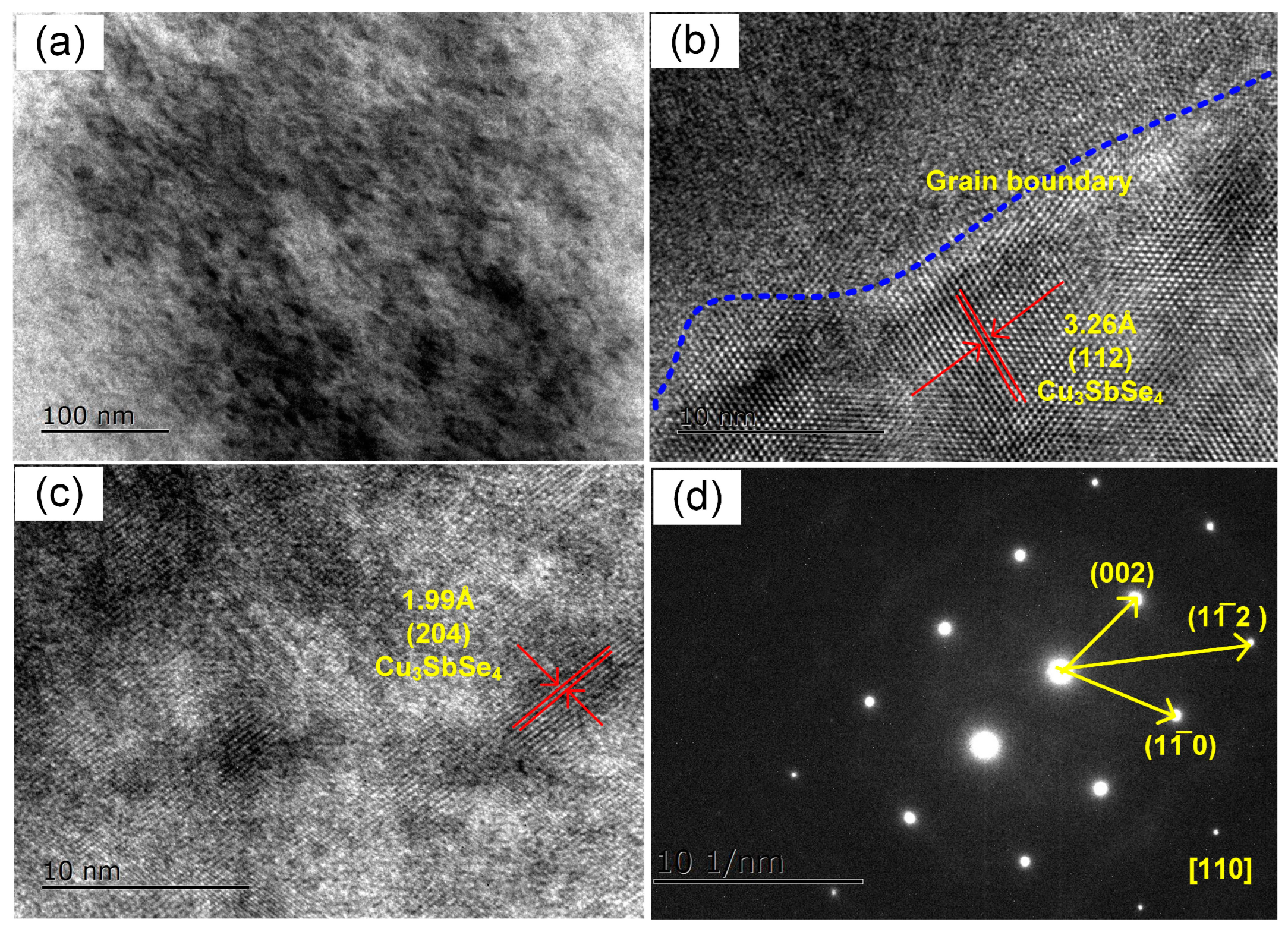
The crystal structures and phase compositions for the Cu3Sb(Se1−xSx)4 (x = 0–1) samples were performed by XRD. Figure 1a shows the crystal structure of tetragonal Cu3SbSe4, with blue, gray, and green atoms representing Cu, Sb, and Se, respectively. As displayed in Figure 1b, the major diffraction peaks of the pristine sample (x = 0) are fully indexed to the zinc-blende-based tetragonal structure (I-42m space group) of Cu3SbSe4 (JCPDS No. 85-0003) without any detectable impurities [29]. With increasing S content (0 < x < 1), a continuous shift of the (112) diffraction peak towards higher angles can be seen (Figure 1c), demonstrating that S atoms replace Se at the Se site to form Cu3Sb(Se1−xSx)4 solid solutions. The shift in the diffraction peak can be ascribed to the smaller radius of S2− (1.84 Å) in comparison to Se2− (1.98 Å) [46]. For x = 1, the XRD peaks match the pattern of Cu3SbS4 (JCPDS No. 35-0581) [47].
The Rietveld refinement profiles of the Cu3Sb(Se1−xSx)4 (x = 0.3) samples based on the famatinite crystal structure are shown in Figure 1d. The data of the final agreement factors (Rp, Rwp, and Rexp) of Cu3Sb(Se1−xSx)4 (x = 0–1) samples are listed in Table S2. The lattice parameter exhibits a linear decrease with increasing S concentration, and closely follows the expected Vegard’s law relationship [48] (Figure 1e), indicating the formation of Cu3SbSe4-Cu3SbS4 solid solutions.

3.2. Microstructure

The morphologies and chemical compositions of the Cu3Sb(Se1−xSx)4 (x = 0.3) sample were characterized by a SEM equipped with an EDS detector (Figure 2). As presented in Figure 2a,b, the SEM images of fracture surfaces (x = 0.3) indicated that they were isotropic materials. The nanopores (marked by the blue dotted circles) were observed on the fracture surface due to the Se/S volatilization of the synthesis process of the sample (Figure 2a), which can contribute to blocking the transport of mid-wavelength phonons [47]. To investigate the composition of the sample, we observed its polished surface (Figure 2c). According to the EDS elemental mapping (Figure 2d–h), the four constituent elements were uniformly distributed with no distinct micro-sized aggregations. This was combined with a back-scattered electron (BSE) image and elemental ratios (%), where Cu, Sb, Se, and S were present in proportions of 40.07:12.68:31.26:15.59 (as depicted in Figure S1), which demonstrated the formation of the Cu3SbSe4-Cu3SbS4 (x = 0.3) solid solution.
The morphologies and compositions of Cu3Sb(Se1−xSx)4 (x = 0.3) were further investigated at nanoscale using high-resolution TEM (HRTEM) (Figure 3). The TEM images demonstrated that many nanophases were distributed in the sample, and elemental mapping taking over the entire region revealed that the four constituent elements (Cu, Sb, Se, and S) were uniformly dispersed within the Cu3SbSe4-Cu3SbS4 solid solution (Figure 3a and Figure S2). As presented in Figure 3b, the grain boundary (indicated by blue dot lines) could be clearly observed in the sample. Meanwhile, as shown in Figure 3b,c, the crossed fringes, with interplanar spacing of 3.26 Å and 1.99 Å corresponded to the (112) and (204) planes of Cu3SbSe4, respectively [49]. Additionally, the SAED pattern taken from the Figure 3c along the [110] zone axis is displayed in Figure 3d. The ordered diffraction spots can be indexed to the (002), (1 1 ¯ 0), and (1 1 ¯ 2) planes of Cu3SbSe4, whose interplanar spacings are 5.64 Å, 4.06 Å, and 3.26 Å, respectively [50].

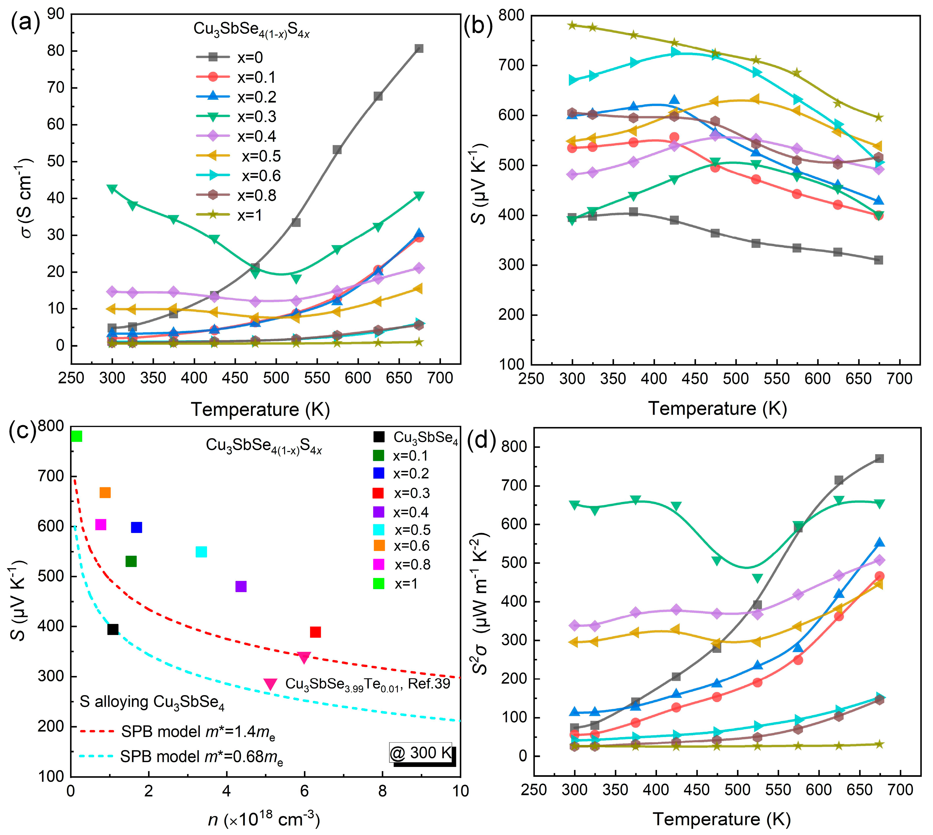
3.3. Charge Transport Properties

To explore the effects of S alloying on the TE properties of the Cu3Sb(Se1−xSx)4 (x = 0–1) solid solutions, the charge transport properties were conducted. The temperature dependence of electrical conductivity (σ) of the Cu3Sb(Se1−xSx)4 (x = 0–1) solid solutions is displayed in Figure 4a. The pristine Cu3SbSe4 exhibited a monotonous increase in σ with rising temperature, demonstrating characteristic behavior of a non-degenerate semiconductor. For the x > 0.2 samples, the samples showed a transition from non-degenerate semiconductors to a partially degenerate regime [51]. The σ exhibited an initial decrease followed by an increase, with the minimum value occurring at ~473 K, indicating its association with bipolar conduction [38,52]. The σ of S alloying samples increased with the S contents until x = 0.3, after which it started to decrease with a higher S content. Notably, the σ improved from ~4.6 S/cm of pristine Cu3SbSe4 to ~42 S/cm of x = 0.3 solid solution at room temperature, arising from the augmented carrier concentration (Table S1). It is worth noting that the solid solutions with high S content (x > 0.5) had lower σ compared to the pristine Cu3SbSe4, which was ascribed to the reduced n (carrier concentration) and diminished μ (carrier mobility). Furthermore, due to the intensified lattice vibration at elevated temperatures, the solid solutions exhibited lower σ than the pristine sample at high temperatures, indicating that the intensified lattice vibration in the solid solutions at elevated temperatures hindered the carrier migration [40,53].
Figure 4b illustrates the temperature-dependent S of the Cu3Sb(Se1−xSx)4 (x = 0–1) samples. The p-type semiconductor behavior of solid solutions, characterized by dominant hole carriers, was evidenced by the positive S value observed across the entire temperature range.
Notably, the S value of the samples exhibited an initial ascent followed by a subsequent descent as the temperature rose, ultimately reaching its zenith at ~473 K. This behavior can be attributed to the influence of the bipolar effect [54]. The maximum S of ~730 μVK−1 was obtained from the x = 0.6 solid solution. We calculated the Eg of the Cu3Sb(Se1−xSx)4 (x = 0–1) samples with the formula: Eg = 2eSmaxT, where Eg, e, Smax, and T represent the band gap, elementary charge, maximal Seebeck coefficient, and the associated temperature, respectively [55]. The calculated Eg for the pristine Cu3SbSe4 of ~0.30 eV aligned well with the reported literature [36,56]; the results are displayed in Figure S3. Consequently, the introduction of alloyed S played a role in enlarging Eg from ~0.30 eV to ~0.69 eV, thus widening the band gap to alleviate the bipolar effect. For the semiconductors, we note that the increase in S (|S|) was directly proportional to the carrier effective mass and n−2/3. We calculated the Pisarenko relation between |S| and n (indigo and red dashed lines with m* ~ 0.68 and 1.4 me, respectively) based on the single parabolic band model (SPB), as follows [57,58]:
S = 8 π 2 k B 2 3 e 2 m * T ( π 3 n ) 2 / 3
where kB, ℏ represent the Boltzmann constant, and Planck constant, respectively. The calculated m* was significantly enhanced from 0.68 for pristine Cu3SbSe4 to 5.03 me for the x = 0.6 sample (Table S1). As seen in Figure 4c, the calculated m* based on S (experimental values) of Cu3Sb(Se1−xSx)4 (x = 0.1–1) samples were above the Pisarenko line. Furthermore, the m* depended directly on the Eg ( 2 k B 2 2 m * = Ε ( 1 + Ε Ε g ) ), where E the energy of electron states), which deviated from a single Kane band model [21,59,60], thus confirming the large S was related to Eg and m*. Consequently, the decreased carrier concentration (x > 0.5) and increased m*, resulted in the significant enhancement of S.
The temperature dependence of the power factors (S2σ) of the Cu3Sb(Se1−xSx)4 (x = 0–1) samples are presented in Figure 4d. The S2σ of Cu3SbSe4-Cu3SbS4 solid solutions exhibited a similar temperature-dependent behavior as the electrical conductivity (σ). The temperature-dependent trend observed in the S2σ was mirrored in the behavior of the σ for the Cu3SbSe4-Cu3SbS4 solid solutions. Owing to their relatively elevated σ and S values, these samples demonstrated larger S2σ values compared to the pristine Cu3SbSe4, particularly within the lower temperature range. Notably, the x = 0.3 sample achieved a larger S2σ value than the other samples, and the peak S2σ value of Cu3SbSe2.8S1.2 sample was ~670 μW m−1 K−2 at 673 K.

3.4. Thermal Transport Properties

The temperature dependence of the thermal transport properties of the Cu3Sb(Se1−xSx)4 (x = 0–1) solid solutions are presented in Figure 5 and Figure S4. Obviously, the κtot decreased with increasing temperature, mainly attributed to the increased scattering by lattice vibrations at elevated temperatures [8,40,53] (Figure 5a). For instance, the κtot of pristine Cu3SbSe4 decreased from ~3.11 Wm−1K−1 at 300 K to ~1.03 Wm−1K−1 at 673 K. Similarly, the κtot of the x = 0.5 sample decreased from ~1.37 Wm−1K−1 at 300 K to ~0.52 Wm−1K−1 at 673 K. Generally, the κlat can be obtained by subtracting the electronic part (κele) from the κtot using the Wiedeman–Franz relationship (the details are displayed in Supplementary Material) [61,62]:
κ   ele = L σ   Τ
where L is the Lorenz number and it can be expressed as Equation (3) [63,64]:
L = 1.5 + exp   [ | S | 116 ]
The calculated L values of the Cu3Sb(Se1−xSx)4 (x = 0–1) samples ranged from 1.5 to 1.6 W Ω K−2, and the results are listed in Figure S5. Owing to the enhanced carrier concentration (x < 0.6), the κele showed a slight increase at low temperature after S alloying, as described in Figure 5b. The κlat of the Cu3Sb(Se1−xSx)4 (x = 0–1) samples is plotted in Figure 5c, indicating a significant decrease within the measured temperature range after S alloying.
To explore the effects of S alloying on the phonon scattering and the significant reduction in κlat, the κlat of the Cu3Sb(Se1−xSx)4 (x = 0–1) compounds was evaluated at room temperature by the Debye–Callaway model. The primary scattering mechanisms under consideration were point defect scattering and Umklapp scattering. Then, the κlat of the pristine ( κ l a t p r i s t i n e ) and S-alloyed (κlat) Cu3SbSe4 compounds could be computed based on the Debye–Callaway model [48,65,66]:
κ lat κ lat pristine = arctan ( u ) u ,   u 2 = π 2 θ D Ω h v 2 κ lat pristine Γ
where u, θD, Ω, h, and ν represent the scaling parameter, Debye temperature, volume per atom, Planck constant, and average speed of sound, respectively (herein, θD = 131 K and ν= 1991.2 m/s [46]). Γ is the imperfection scale parameter, which is associated with the Γm (mass fluctuation) and Γs (strain field fluctuation) [67]:
Γ = Γ m + Γ s = x ( 1 x ) [ ( Δ M M ) 2 + ε ( Δ r r ) 2 ]
where x, ∆M/M and ∆r/r are the S concentration in one molecular, the relative change of atomic mass, and atomic radius owing to the replacement of Se with S, respectively. The ε value can be computed using the following formula [68]:
ε = 2 9 ( 6 . 4 γ ( 1 + υ p ) 1 υ p ) 2
where, γ and υp are the Grüneisen parameter and Poisson ratio, respectively (here, γ = 1.3 [46] and υp = 0.35 [69]).
The values of Γm and Γs for the Cu3Sb(Se1−xSx)4 compounds are presented in Table S3. Figure 5d shows how the scattering parameters Γm and Γs changed with varying Se-alloying levels. It was observed that Γm was smaller than Γs when the S content x ≤ 0.6, indicating that the Γs (strain field fluctuation) contributed greatly to the drop of κlat. As for the x > 0.6 samples, the Γm (mass fluctuation) was the dominant. It is commonly accepted that the atomic radius of S is different from that of the Se atom, inducing a localized lattice distortion and leading to local field fluctuations that hinder the propagation of heat-carrying phonons [70,71]. However, with increasing S content, the mass fluctuation gradually became the dominant factor. The experimental κlat closely aligned with the curve calculated by the Callaway model (Figure 5e), suggesting that point defects made a great contribution to suppress the κlat in the Cu3Sb(Se1−xSx)4 solid solutions [48]. For a more comprehensive evaluation of our results, a comparison of the our κlat data with the recently reported values of Cu3SbSe4 are illustrated in Figure 5f [33,34,36,38,39]. Remarkably, the Cu3Sb(Se1−xSx)4 (x = 0.5) sample achieved an outstandingly low κlat of ~0.50 W m−1 K−1 at 673 K.

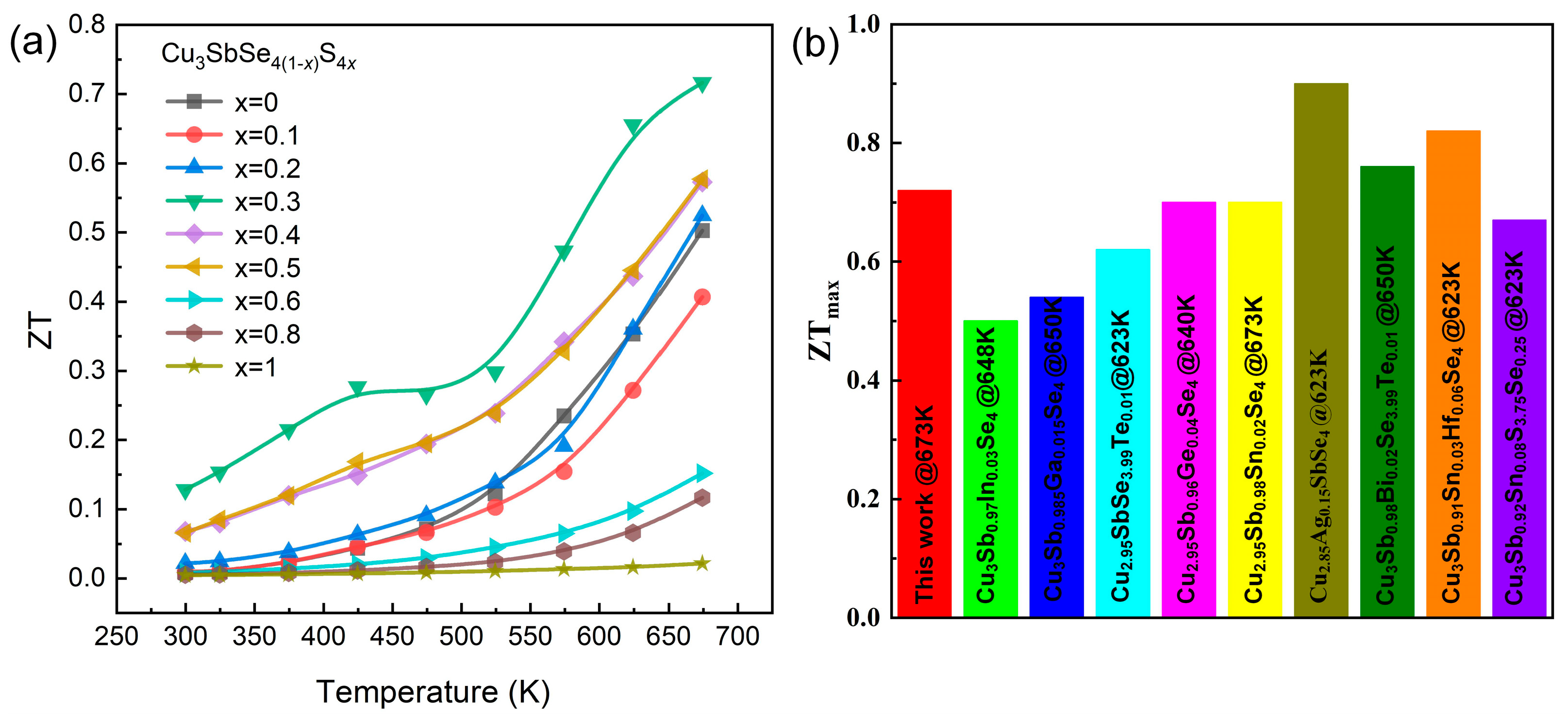
3.5. Figure of Merit (ZT)

The temperature-dependent ZT of the Cu3Sb(Se1−xSx)4 (x = 0–1) samples are illustrated in Figure 6a. With the benefit of the collaborative enhancement of electrical and thermal transport properties, the x = 0.3 sample attained a maximum ZT value of ~0.72 at 673 K, which was 44% higher than that of pristine Cu3SbSe4. To further analyze our TE properties, the comparison of the ZTmax of the Cu3SbSe4-based materials is given in Figure 6b [33,34,35,36,37,38,39,40,72]. Obviously, our ZTmax of 0.72 was higher than that of other Cu3SbSe4-based materials, such as Cu3Sb0.97In0.03Se4 ~0.5, Cu3Sb0.985Ga0.015Se4 ~0.54, Cu3SbSe3.99Te0.01 ~0.62, Cu3Sb0.92Sn0.08S3.75Se0.25 ~0.67, Cu2.95Sb0.96Ge0.04Se4 ~0.70, and Cu2.95Sb0.98Sn0.02Se4 ~0.7 and is comparable to the ZT values for Cu3Sb0.98Bi0.02Se3.99Te0.01 ~0.76 and Cu3Sb0.91Sn0.03Hf0.06Se4 ~0.76. Although the Cu3Sb(Se1−xSx)4 (x = 0–1) samples had relative low ZT values in comparison with other high-performance TE materials, further enhancements of the ZT values can potentially be achieved by tuning the carrier concentration, dual-incorporation, and/or introducing band engineering.

4. Conclusions

In summary, a series of Cu3SbSe4-Cu3SbS4 solid solutions were synthesized by vacuum melting and plasma-activated sintering (PAS) techniques, and the effects of S alloying on TE performance were investigated. S alloying can widen the band gap, effectively alleviating the bipolar effect. Additionally, the S (Seebeck coefficient) was significantly improved because of the increased m*. Furthermore, the substitution of S for Se in Cu3SbSe4 lattice led to noticeable local distortions, yielding large strain and mass fluctuations to suppress the κlat, thus decreasing the κlat and κtot to ~0.50 Wm−1K−1 and ~0.52 Wm−1K−1 at 673 K, respectively. Consequently, a peak ZT value of ~0.72 was obtained at 673 K for the Cu3Sb(Se1−xSx)4 (x = 0.3) sample. Based on these results, it is speculated that further improvement in the figure of merit of Cu3Sb(Se1−xSx)4 solid solutions can be obtained by enhanced electrical transport properties. Our research offers a new strategy to develop high-performance TE materials in solid solutions via elemental alloying.

Supplementary Materials

The supporting information can be downloaded at: https://www.mdpi.com/article/10.3390/nano13192730/s1.

Author Contributions

Conceptualization, L.Z., J.Y., B.G., L.Y., Z.S., A.M.K., S.D., S.H., G.Q. and J.X.; Methodology, L.Z., H.H., J.Y., X.W., B.G., G.Q. and J.X.; Validation, Z.L. and S.H.; Formal analysis, L.Z., J.Y., X.W., B.G., L.Y., Z.S., A.M.K., S.D. and G.Q.; Investigation, L.Z., H.H., Z.L. and X.W.; Resources, J.Y. and J.X.; Data curation, B.G., Z.S., A.M.K. and S.H.; Writing—original draft, L.Z., H.H. and Z.L.; Writing—review & editing, J.Y.; Visualization, S.D.; Supervision, L.Y., G.Q. and J.X.; Project administration, S.H.; Funding acquisition, L.Y., G.Q. and J.X. All authors have read and agreed to the published version of the manuscript.

Funding

This work was funded by the National Natural Science Foundation of China (51572111, 52071159, 52172090), the Natural Science Foundation (BK20210779), the University-Industry Research Cooperation Project (BY20221151), and the Universities Natural Science Research Project (21KJB430019) of Jiangsu Province. This work was also funded by the Researchers Supporting Project Number (RSPD2023R764), King Saud University, Riyadh, Saudi Arabia.

Data Availability Statement

Data will be made available on reasonable request.

Conflicts of Interest

The authors declare that they have no known competing financial interests or personal relationships that could have appeared to influence the work reported in this paper.

References

  1. Bell, L.E. Cooling, heating, generating power, and recovering waste heat with thermoelectric systems. Science 2008, 321, 1457–1461. [Google Scholar] [CrossRef]
  2. Snyder, G.J.; Toberer, E.S. Complex thermoelectric materials. Nat. Mater. 2011, 473, 66–69. [Google Scholar]
  3. Shi, X.L.; Zou, J.; Chen, Z.-G. Advanced thermoelectric design: From materials and structures to devices. Chem. Rev. 2020, 120, 7399–7515. [Google Scholar]
  4. DiSalvo, F.J. Termoelectric cooling and power generation. Science 1999, 285, 703–706. [Google Scholar] [CrossRef] [PubMed]
  5. Tang, Y.L.; Gibbs, Z.M.; Agapito, L.A.; Li, G.D.; Kim, H.S.; Nardelli, M.B.; Curtarolo, S.; Snyder, G.J. Convergence of multi-valley bands as the electronic origin of high thermoelectric performance in CoSb3 skutterudites. Nat. Mater. 2015, 14, 1223–1228. [Google Scholar] [PubMed]
  6. Fu, C.G.; Bai, S.Q.; Liu, Y.T.; Tang, Y.S.; Chen, L.D.; Zhao, X.B.; Zhu, T.J. Realizing high figure of merit in heavy-band p-type half-Heusler thermoelectric materials. Nat. Commun. 2015, 6, 8144. [Google Scholar] [PubMed]
  7. Song, J.; Song, H.Y.; Wang, Z.; Lee, S.; Hwang, J.Y.; Lee, S.Y.; Lee, J.; Kim, D.; Lee, K.H.; Kim, Y.; et al. Creation of two-dimensional layered Zintl phase by dimensional manipulation of crystal structure. Sci. Adv. 2019, 5, eaax0390. [Google Scholar]
  8. Zhou, C.J.; Lee, Y.K.; Yu, Y.; Byun, S.J.; Luo, Z.Z.; Lee, H.; Ge, B.Z.; Lee, Y.L.; Chen, X.Q.; Lee, J.Y.; et al. Polycrystalline SnSe with a thermoelectric figure of merit greater than the single crystal. Nat. Mater. 2021, 20, 1378–1384. [Google Scholar]
  9. Zhang, L.; Hong, X.; Chen, Z.Q.; Xiong, D.K.; Bai, J.M. Effects of In2O3 nanoparticles addition on microstructures and thermoelectric properties of Ca3Co4O9 compounds. Ceram. Int. 2020, 46, 17763–17766. [Google Scholar] [CrossRef]
  10. Dong, S.-T.; Yu, M.-C.; Fu, Z.; Lv, Y.-Y.; Yao, S.-H.; Chen, Y.B. High thermoelectric performance of NaF-doped Bi2Ca2Co2Oy ceramic samples. J. Mater. Res. Technol. 2022, 17, 1598–1604. [Google Scholar] [CrossRef]
  11. Jiang, B.B.; Yu, Y.; Cui, J.; Liu, X.X.; Xie, L.; Liao, J.C.; Zhang, Q.H.; Huang, Y.; Ning, S.C.; Jia, B.H.; et al. High-entropy-stabilized chalcogenides with high thermoelectric performance. Science 2021, 371, 830–834. [Google Scholar] [CrossRef] [PubMed]
  12. He, J.; Tritt, T.M. Advances in thermoelectric materials research: Looking back and moving forward. Science 2017, 357, 1369. [Google Scholar]
  13. Yang, X.; Wang, C.Y.; Lu, R.; Shen, Y.N.; Zhao, H.B.; Li, J.; Li, R.Y.; Zhang, L.X.; Chen, H.S.; Zhang, T.; et al. Progress in measurement of thermoelectric properties of micro/nano thermoelectric materials: A critical review. Nano Energy 2022, 101, 107553. [Google Scholar]
  14. Lan, R.; Otoo, S.L.; Yuan, P.Y.; Wang, P.F.; Yuan, Y.Y.; Jiang, X.B. Thermoelectric properties of Sn doped GeTe thin films. Appl. Surf. Sci. 2020, 507, 145025. [Google Scholar]
  15. Pei, Y.Z.; Shi, X.Y.; LaLonde, A.; Wang, H.; Chen, L.D.; Snyder, G.J. Convergence of electronic bands for high performance bulk thermoelectrics. Nature 2011, 473, 66–69. [Google Scholar] [PubMed]
  16. Zhang, Q.; Song, Q.C.; Wang, X.Y.; Sun, J.Y.; Zhu, Q.; Dahal, K.; Lin, X.; Cao, F.; Zhou, J.W.; Chen, S.; et al. Deep defect level engineering: A strategy of optimizing the carrier concentration for high thermoelectric performance. Energy Environ. Sci. 2018, 11, 933–940. [Google Scholar] [CrossRef]
  17. Cheng, C.; Zhao, L.D. Anharmoncity and low thermal conductivity in thermoelectrics. Mater. Today Phys. 2018, 4, 50–57. [Google Scholar]
  18. Zhao, H.B.; Yang, X.; Wang, C.Y.; Lu, R.; Zhang, T.; Chen, H.S.; Zheng, X.H. Progress in thermal rectification due to heat conduction in micro/nano solids. Mater. Today Phys. 2023, 30, 100941. [Google Scholar]
  19. Biswas, K.; He, J.Q.; Blum, I.D.; Wu, C.I.; Hogan, T.P.; Seidman, D.N.; Dravid, V.P.; Kanatzidis, M.G. High-performance bulk thermoelectrics with all-scale hierarchical architectures. Nature 2012, 489, 414–418. [Google Scholar] [CrossRef]
  20. Kim, S.; Lee, K.H.; Mun, H.A.; Kim, H.S.; Hwang, S.W.; Roh, J.W.; Yang, D.J.; Shin, W.H.; Li, X.S.; Lee, Y.H.; et al. Dense dislocation arrays embedded in grain boundaries for high-performance bulk thermoelectrics. Science 2015, 348, 109–114. [Google Scholar] [CrossRef]
  21. Tan, G.J.; Zhao, L.D.; Kanatzidis, M.G. Rationally designing high-performance bulk thermoelectric materials. Chem. Rev. 2016, 116, 12123–12149. [Google Scholar]
  22. Liu, H.L.; Shi, X.; Xu, F.F.; Zhang, L.L.; Zhang, W.Q.; Chen, L.D.; Li, Q.; Uher, C.; Day, T.; Snyder, G.J. Copper ion liquid-like thermoelectrics. Nat. Mater. 2012, 11, 422–425. [Google Scholar] [CrossRef]
  23. Qiu, P.F.; Shi, X.; Chen, L.D. Cu-based thermoelectric materials. Energy Storage Mater. 2016, 3, 85–97. [Google Scholar]
  24. Bo, L.; Li, F.J.; Hou, Y.B.; Zuo, M.; Zhao, D.G. Enhanced thermoelectric performance of Cu2Se via nanostructure and compositional gradient. Nanomaterials 2022, 12, 640. [Google Scholar] [CrossRef] [PubMed]
  25. Ge, B.Z.; Lee, H.; Zhou, C.J.; Lu, W.Q.; Hu, J.B.; Yang, J.; Cho, S.-P.; Qiao, G.; Shi, Z.; Chung, I. Exceptionally low thermal conductivity realized in the chalcopyrite CuFeS2 via atomic-level lattice engineering. Nano Energy 2022, 94, 106941. [Google Scholar]
  26. Kumar, V.P.; Paradis-Fortin, L.; Lemoine, P.; Caër, G.L.; Malaman, B.; Boullay, P.; Raveau, B.; Guélou, G.; Guilmeau, E. Crossover from germanite to renierite-type structures in Cu22–xZnxFe8Ge4S32 thermoelectric sulfides. ACS Appl. Energy Mater. 2019, 2, 7679–7689. [Google Scholar] [CrossRef]
  27. Hagiwara, T.; Suekuni, K.; Lemoine, P.; Supka, A.R.; Chetty, R.; Guilmeau, E.; Raveau, B.; Fornari, M.; Ohta, M.; Orabi, R.R.; et al. Key role of d0 and d10 cations for the design of semiconducting colusites: Large thermoelectric ZT in Cu26Ti2Sb6S32 compounds. Chem. Mater. 2021, 33, 3449–3456. [Google Scholar] [CrossRef]
  28. Guélou, G.; Lemoine, P.; Raveau, B.; Guilmeau, E. Recent developments in high-performance thermoelectric sulphides: An overview of the promising synthetic colusites. J. Mater. Chem. 2021, 9, 773–795. [Google Scholar]
  29. Yang, C.Y.; Huang, F.Q.; Wu, L.M.; Xu, K. New stannite-like p-type thermoelectric material Cu3SbSe4. J. Phys. D Appl. Phys. 2011, 44, 295404. [Google Scholar] [CrossRef]
  30. Do, D.T.; Mahanti, S.D. Theoretical study of defects Cu3SbSe4: Search for optimum dopants for enhancing thermoelectric properties. J. Alloys Compd. 2015, 625, 346–354. [Google Scholar] [CrossRef]
  31. Huang, Y.L.; Zhang, B.; Li, J.W.; Zhou, Z.Z.; Zheng, S.K.; Li, N.H.; Wang, G.W.; Zhang, D.; Zhang, D.L.; Han, G.; et al. Unconventional doping effect leads to ultrahigh average thermoelectric power factor in Cu3SbSe4-Based composites. Adv. Mater. 2022, 34, 2109952. [Google Scholar] [CrossRef] [PubMed]
  32. García, G.; Palacios, P.; Cabot, A.; Wahnón, P. Thermoelectric properties of doped-Cu3SbSe4 compounds: A first-principles insight. Inorg. Chem. 2018, 57, 7321–7333. [Google Scholar] [CrossRef]
  33. Zhang, D.; Yang, J.Y.; Jiang, Q.H.; Fu, L.W.; Xiao, Y.; Luo, Y.B.; Zhou, Z.W. Improvement of thermoelectric properties of Cu3SbSe4 compound by in doping. Mater. Des. 2016, 98, 150–154. [Google Scholar] [CrossRef]
  34. Zhao, D.G.; Wu, D.; Bo, L. Enhanced thermoelectric properties of Cu3SbSe4 compounds via Gallium doping. Energies 2017, 10, 1524. [Google Scholar] [CrossRef]
  35. Chang, C.H.; Chen, C.L.; Chiu, W.T.; Chen, Y.Y. Enhanced thermoelectric properties of Cu3SbSe4 by germanium doping. Mater. Lett. 2017, 186, 227–230. [Google Scholar] [CrossRef]
  36. Wei, T.R.; Wang, W.H.; Gibbs, Z.M.; Wu, C.F.; Snyder, G.J.; Li, J.-F. Thermoelectric properties of Sn-doped p-type Cu3SbSe4: A compound with large effective mass and small band gap. J. Mater. Chem. A 2014, 2, 13527–13533. [Google Scholar] [CrossRef]
  37. Kumar, A.; Dhama, P.; Banerji, P. Enhanced thermoelectric properties in Bi and Te doped p-type Cu3SbSe4 compound. In Proceedings of the DAE Solid State Physics Symposium 2017, Mumbai, India, 26–30 December 2017; Volume 1942, p. 140080. [Google Scholar]
  38. Zhang, D.; Yang, J.Y.; Bai, H.C.; Luo, Y.B.; Wang, B.; Hou, S.H.; Li, Z.L.; Wang, S.F. Significant average ZT enhancement in Cu3SbSe4-based thermoelectric material via softening p-d hybridization. J. Mater. Chem. A 2019, 7, 17655–17656. [Google Scholar] [CrossRef]
  39. Zhang, D.; Yang, J.Y.; Jiang, Q.H.; Zhou, Z.W.; Li, X.; Ren, Y.Y.; Xin, J.W.; Basit, A.; He, X.; Chu, W.J.; et al. Simultaneous optimization of the overall thermoelectric properties of Cu3SbSe4 by band engineering and phonon blocking. J. Alloys Compd. 2017, 724, 597–602. [Google Scholar] [CrossRef]
  40. Wang, B.Y.; Zheng, S.Q.; Wang, Q.; Li, Z.L.; Li, J.; Zhang, Z.P.; Wu, Y.; Zhu, B.S.; Wang, S.Y.; Chen, Y.X.; et al. Synergistic modulation of power factor and thermal conductivity in Cu3SbSe4 towards high thermoelectric performance. Nano Energy 2020, 71, 104658. [Google Scholar] [CrossRef]
  41. Xie, D.D.; Zhang, B.; Zhang, A.J.; Chen, Y.J.; Yan, Y.C.; Yang, H.Q.; Wang, G.W.; Wang, G.Y.; Han, X.D.; Han, G.; et al. High thermoelectric performance of Cu3SbSe4 nanocrystals with Cu2-xSe in situ inclusions synthesized by a microwave-assisted solvothermal method. Nanoscale 2018, 10, 14546–14553. [Google Scholar] [CrossRef] [PubMed]
  42. Zhao, L.J.; Yu, L.H.; Yang, J.; Wang, M.Y.; Shao, H.C.; Wang, J.L.; Shi, Z.Q.; Wan, N.; Hussain, S.; Qiao, G.J.; et al. Enhancing thermoelectric and mechanical properties of p-type Cu3SbSe4-based materials via embedding Nanoscale Sb2Se3. Mater. Chem. Phys. 2022, 292, 126669. [Google Scholar]
  43. Skoug, E.J.; Cain, J.D.; Morelli, D.T. Thermoelectric properties of the Cu2SnSe3–Cu2GeSe3 solid solution. J. Alloys Compd. 2010, 506, 18–21. [Google Scholar] [CrossRef]
  44. Jacob, S.; Delatouche, B.; Péré, D.; Jacoba, A.; Chmielowski, R. Insights into the thermoelectric properties of the Cu2Ge(S1−xSex)3 solid solutions. Mater. Today Proc. 2017, 4, 12349–12359. [Google Scholar]
  45. Wang, R.F.; Dai, L.; Yan, Y.C.; Peng, K.L.; Lu, X.; Zhou, X.Y.; Wang, G.Y. Complex alloying effect on thermoelectric transport properties of Cu2Ge(Se1−xTex)3. Chin. Phys. B 2018, 27, 067201. [Google Scholar]
  46. Skoug, E.J.; Cain, J.D.; Morelli, D.T. High thermoelectric figure of merit in the Cu3SbSe4-Cu3SbS4 solid solution. Appl. Phys. Lett. 2011, 98, 261911. [Google Scholar] [CrossRef]
  47. Lu, B.B.; Wang, M.Y.; Yang, J.; Hou, H.G.; Zhang, X.Z.; Shi, Z.Q.; Liu, J.L.; Qiao, G.J.; Liu, G.W. Dense twin and domain boundaries lead to high thermoelectric performance in Sn-doped Cu3SbS4. Appl. Phys. Lett. 2022, 120, 173901. [Google Scholar]
  48. Zhao, K.P.; Blichfeld, A.B.; Eikeland, E.; Qiu, P.F.; Ren, D.D.; Iversen, B.B.; Shi, X.; Chen, L.D. Extremely low thermal conductivity and high thermoelectric performance in liquid-like Cu2Se1−xSx polymorphic materials. J. Mater. Chem. A 2017, 5, 18148–18156. [Google Scholar]
  49. Li, J.M.; Ming, H.W.; Song, C.J.; Wang, L.; Xin, H.X.; Gu, Y.J.; Zhang, J.; Qin, X.Y.; Li, D. Synergetic modulation of power factor and thermal conductivity for Cu3SbSe4-based system. Mater. Today Energy 2020, 18, 100491. [Google Scholar]
  50. Zhou, T.; Wang, L.J.; Zheng, S.Q.; Hong, M.; Fang, T.; Bai, P.P.; Chang, S.Y.; Cui, W.L.; Shi, X.L.; Zhao, H.Z.; et al. Self-assembled 3D flower-like hierarchical Ti-doped Cu3SbSe4 microspheres with ultralow thermal conductivity and high zT. Nano Energy 2018, 49, 221–229. [Google Scholar] [CrossRef]
  51. Li, X.Y.; Li, D.; Xin, H.X.; Zhang, J.; Song, C.J.; Qin, X.Y. Effects of bismuth doping the thermoelectric properties of Cu3SbSe4 at moderate temperatures. J. Alloys Compd. 2013, 561, 105–108. [Google Scholar] [CrossRef]
  52. Bhardwaj, R.; Bhattacharya, A.; Tyagi, K.; Gahtori, B.; Chauhan, N.S.; Bathula, S.; Auluck, S.; Dhar, A. Tin doped Cu3SbSe4: A stable thermoelectric analogue for the mid-temperature applications. Mater. Res. Bull. 2019, 113, 38–44. [Google Scholar]
  53. Yang, J.; Zhang, X.Z.; Liu, G.W.; Zhao, L.J.; Liu, J.L.; Shi, Z.Q.; Ding, J.N.; Qiao, G.J. Multiscale structure and band configuration tuning to achieve high thermoelectric properties in n-type PbS bulks. Nano Energy 2020, 74, 104826. [Google Scholar]
  54. Yang, X.X.; Gu, Y.Y.; Li, Y.P.; Guo, K.; Zhang, J.Y.; Zhao, J.T. The equivalent and aliovalent dopants boosting the thermoelectric properties of YbMg2Sb2. Sci. China Mater. 2020, 63, 437–443. [Google Scholar]
  55. Goldsmid, H.J.; Sharp, J.W. Estimation of the thermal band gap of a semiconductor from Seebeck measurements. J. Electron. Mater. 1999, 28, 869–872. [Google Scholar] [CrossRef]
  56. Skoug, E.J.; Cain, J.D.; Majsztrik, P.; Kirkham, M.; LaraCurzio, E.; Morelli, D.T. Doping effects on the thermoelectric properties of Cu3SbSe4. Sci. Adv. Mater. 2011, 3, 602–606. [Google Scholar] [CrossRef]
  57. Cutler, M.; Leavy, J.F.; Fitzpatrick, R.L. Electronic transport in semimetallic cerium sulfide. Phys. Rev. 1964, 133, A1143–A1152. [Google Scholar]
  58. Wei, T.-R.; Tan, G.; Zhang, X.; Wu, C.-F.; Li, J.-F.; Dravid, V.P.; Snyder, G.J.; Kanatzidis, M.G. Distinct impact of Alkali-Ion doping on electrical transport properties of thermoelectric p-Type polycrystalline SnSe. J. Am. Chem. Soc. 2016, 138, 8875–8882. [Google Scholar] [CrossRef] [PubMed]
  59. Ge, B.Z.; Lee, H.; Im, J.; Choi, Y.; Kim, Y.-S.; Lee, J.Y.; Cho, S.-P.; Sung, Y.-E.; Choi, K.-Y.; Zhou, C.J.; et al. Engineering atomic-level crystal lattice and electronic band structure for extraordinarily high average thermoelectric figure of merit in n-type PbSe. Energy Environ. Sci. 2023, 16, 3994–4008. [Google Scholar] [CrossRef]
  60. Zhou, C.J.; Yu, Y.; Lee, Y.L.; Ge, B.Z.; Lu, W.Q.; Miredin, O.C.; Im, J.; Cho, S.P.; Wuttig, M.; Shi, Z.Q.; et al. Exceptionally high average power factor and thermoelectric figure of merit in n-type PbSe by the dual incorporation of Cu and Te. J. Am. Chem. Soc. 2020, 142, 15172–15186. [Google Scholar] [CrossRef]
  61. Mahan, G.D.; Bartkowiak, M. Wiedemann–Franz law at boundaries. Appl. Phys. Lett. 1999, 74, 953–954. [Google Scholar] [CrossRef]
  62. Fu, Z.; Jiang, J.L.; Dong, S.-T.; Yu, M.-C.; Zhao, L.J.; Wang, L.; Yao, S.-H. Effects of Zr substitution on structure and thermoelectric properties of Bi2O2Se. J. Mater. Res. Technol. 2022, 21, 640–647. [Google Scholar]
  63. Kim, H.S.; Gibbs, Z.M.; Tang, Y.G.; Wang, H.; Snyder, G.J. Characterization of Lorenz number with Seebeck coefficient measurement. APL Mater. 2015, 3, 041506. [Google Scholar]
  64. Wang, B.Y.; Zheng, S.Q.; Chen, Y.X.; Wu, Y.; Li, J.; Ji, Z.; Mu, Y.N.; Wei, Z.B.; Liang, Q.; Liang, J.X. Band Engineering for Realizing Large Effective Mass in Cu3SbSe4 by Sn/La Co-doping. J. Phys. Chem. C 2020, 124, 10336–10343. [Google Scholar]
  65. Callaway, J.; von Baeyer, H.C. Effect of point imperfections on lattice thermal conductivity. Phys. Rev. 1960, 120, 1149–1154. [Google Scholar]
  66. Yang, J.; Meisner, G.P.; Chen, L.D. Strain field fluctuation effects on lattice thermal conductivity of ZrNiSn-based thermoelectric compounds. Appl. Phys. Lett. 2004, 85, 1140–1142. [Google Scholar]
  67. Xie, H.Y.; Su, X.L.; Zheng, G.; Zhu, T.; Yin, K.; Yan, Y.G.; Uher, C.; Kanatzidis, M.G.; Tang, X.F. The role of Zn in chalcopyrite CuFeS2: Enhanced thermoelectric properties of Cu1−xZnxFeS2 with in situ nanoprecipitates. Adv. Energy Mater. 2017, 7, 1601299. [Google Scholar]
  68. Wan, C.L.; Pan, W.; Xu, Q.; Qin, Y.X.; Wang, J.D.; Qu, Z.X.; Fang, M.H. Effect of point defects on the thermal transport properties of (LaxGd1−x)2Zr2O7: Experiment and theoretical model. Phys. Rev. B 2006, 74, 144109. [Google Scholar]
  69. Xu, B.; Zhang, X.D.; Su, Y.Z.; Zhang, J.; Wang, Y.S.; Yi, L. Elastic Anisotropy and Anisotropic Transport Properties of Cu3SbSe4 and Cu3SbS4. J. Phys. Soc. Jpn. 2014, 83, 094606. [Google Scholar]
  70. Yang, J.; Song, R.F.; Zhao, L.J.; Zhang, X.Z.; Hussaina, S.; Liu, G.W.; Shi, Z.Q.; Qiao, G.J. Magnetic Ni doping induced high power factor of Cu2GeSe3-based bulk materials. J. Eur. Ceram. Soc. 2021, 41, 3473–3479. [Google Scholar]
  71. Lu, X.; Morelli, D.T.; Wang, Y.X.; Lai, W.; Xia, Y.; Ozolins, V. Phase stability, crystal structure, and thermoelectric properties of Cu12Sb4S13-xSex solid solutions. Chem. Mater. 2016, 28, 1781–1786. [Google Scholar]
  72. Park, S.J.; Kim, I.H. Enhanced thermoelectric performance of Sn and Se double-doped famatinites. J. Korean Phys. Soc. 2023, 83, 57–64. [Google Scholar]
Figure 1. (a) The crystal structure of Cu3SbSe4; (b) X-ray diffraction (XRD) patterns and (c) magnified diffraction peaks corresponding to the (112) planes of Cu3Sb(Se1−xSx)4 (x = 0–1) samples; (d) Rietveld refinement profile of x = 0.3 solid solution; (e) Alterations in lattice parameters as S concentration varies.
Nanomaterials 13 02730 g001
Figure 2. (a) SEM image of the fracture surfaces of the Cu3SbSe2.8S1.2 sample; (b) high magnification images of (a); (c) the corresponding EDS mapping for all constituent elements of selected region in (b); (c) SEM images of the polished surfaces of the Cu3SbSe2.8S1.2 sample; (d) The corresponding elemental mapping by EDS, obtained by overlaying the respective EDS signals directly arising from Cu (e), Sb (f), Se (g), and S (h).
Nanomaterials 13 02730 g002
Figure 3. (a) The low-magnification image; (b,c) high-resolution TEM images; (d) SAED pattern taken from (c) of Cu3Sb(Se1−xSx)4 (x = 0.3) sample.
Nanomaterials 13 02730 g003
Figure 4. Temperature-dependent (a) electrical conductivity σ; (b) Seebeck coefficient S, the inset is Eg; (c) Pisarenko relationship with m* in this work compared with other works at room temperature. The indigo and red broken line represent the Pisarenko relationship with m* ~ 0.68 and 1.4 me, respectively. (d) power factor S2σ of Cu3Sb(Se1−xSx)4 (x = 0–1) samples.
Nanomaterials 13 02730 g004
Figure 5. Temperature-dependent (a) total thermal conductivity κtot; (b) electronic thermal conductivity κele; (c) lattice thermal conductivity κlat of Cu3Sb(Se1−xSx)4 (x = 0–1) samples, and (d) imperfection scaling parameters; (e) κlat at 300 K, the red dotted lines is calculated by the Callaway model; (f) the comparison of κlat of Cu3SbSe4-based materials [33,34,36,38,39].
Nanomaterials 13 02730 g005
Figure 6. (a) Temperature-dependent figure of merit (ZT); (b) Comparison of ZTmax of Cu3SbSe4-based materials [33,34,35,36,37,38,39,40,72].
Nanomaterials 13 02730 g006
Disclaimer/Publisher’s Note: The statements, opinions and data contained in all publications are solely those of the individual author(s) and contributor(s) and not of MDPI and/or the editor(s). MDPI and/or the editor(s) disclaim responsibility for any injury to people or property resulting from any ideas, methods, instructions or products referred to in the content.

