
Cold Cathodes with Two-Dimensional van der Waals Materials


Abstract
1. Introduction
2. Emitter Structure
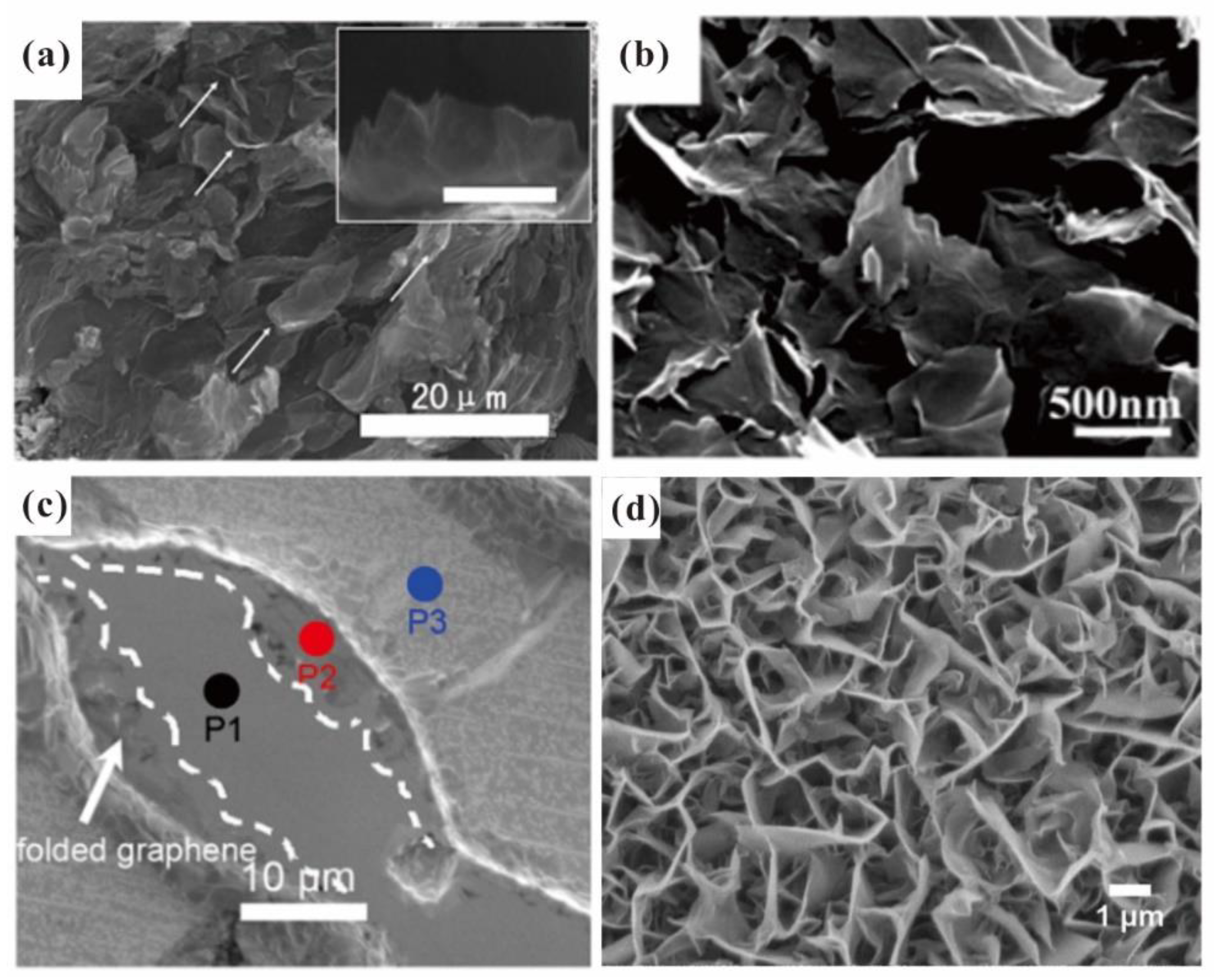
2.1. Edge Emitter
2.1.1. Vertical Emitter
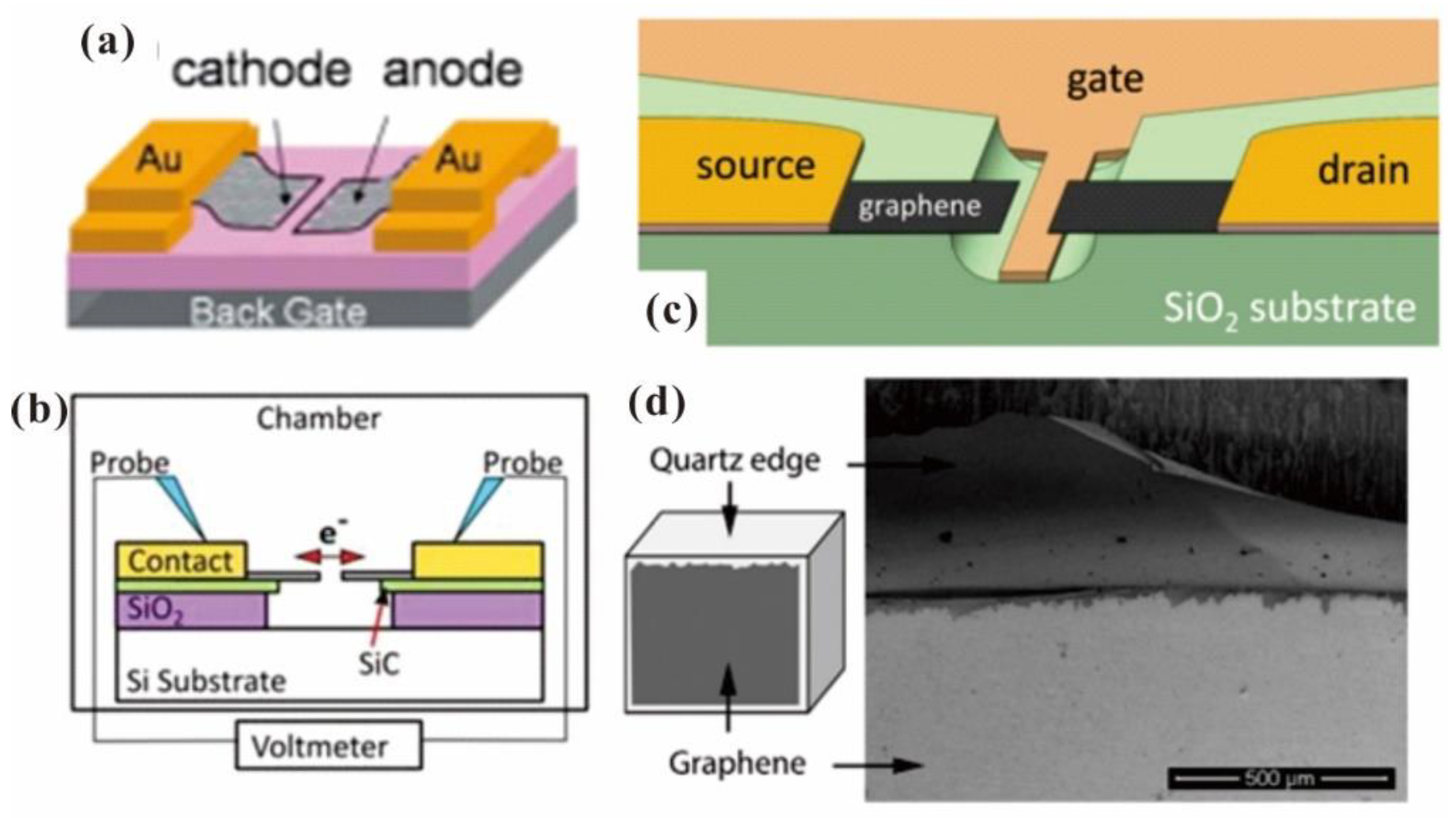
2.1.2. Lateral Emitter Structure
2.2. Surface Emitter
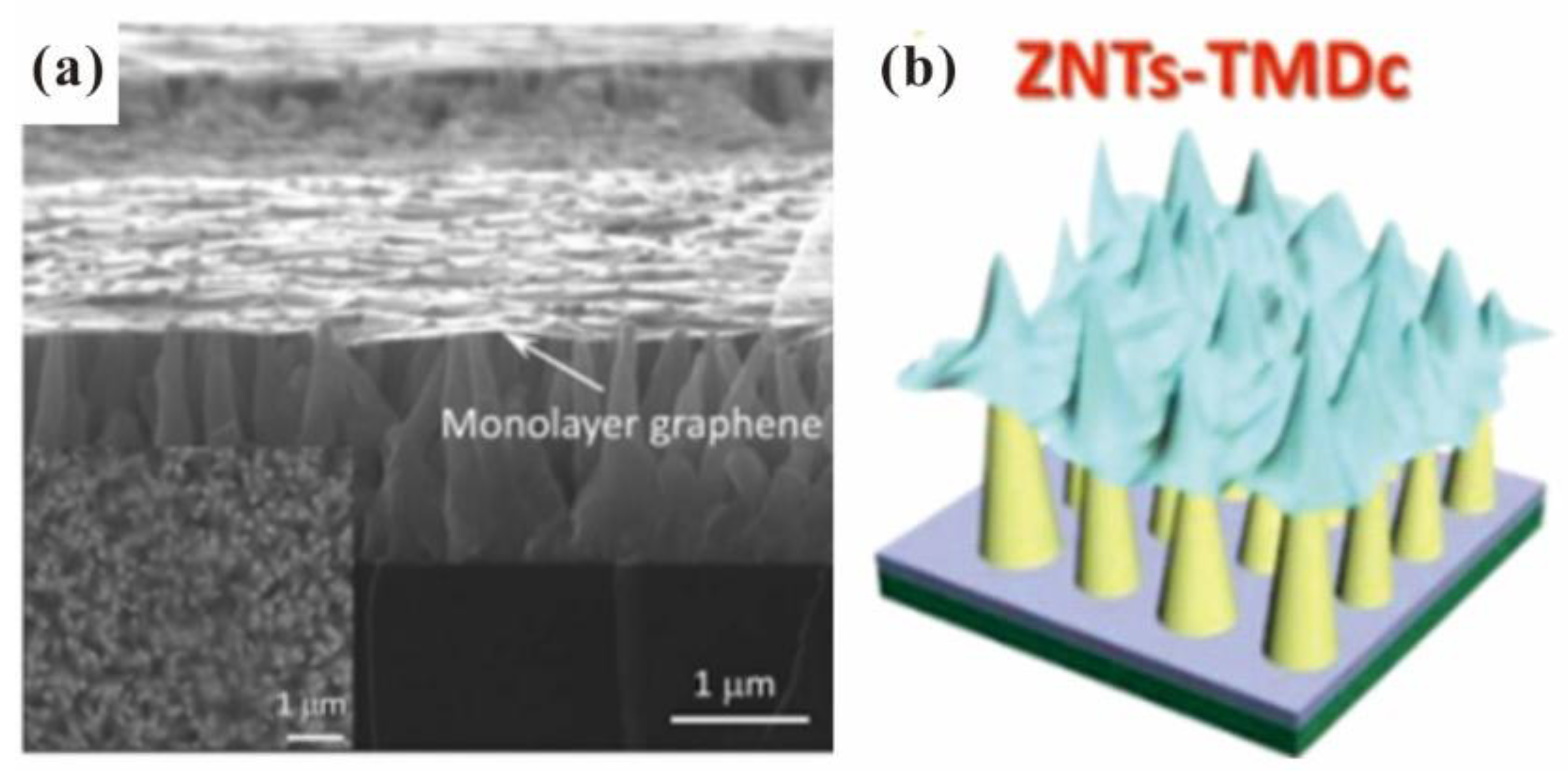
2.2.1. 2D/1D Hybrid Structure
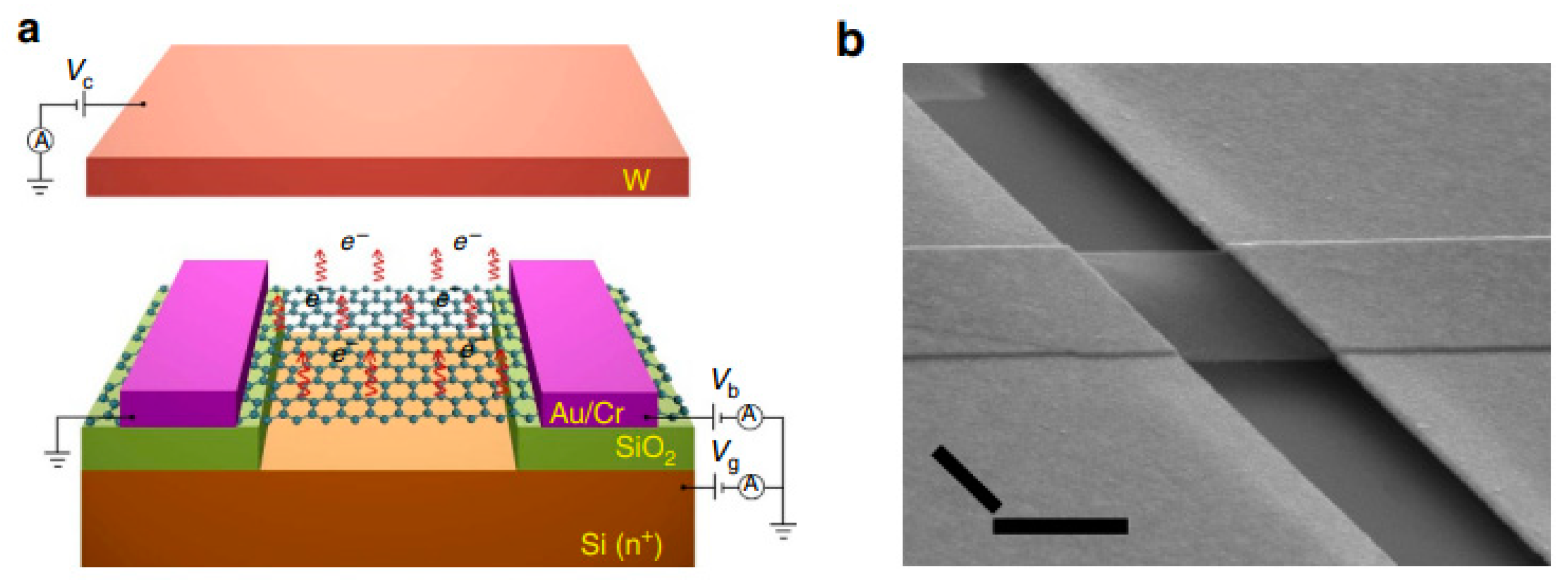
2.2.2. Van der Waals Heterostructure
2.2.3. Suspended Graphene Structure
3. Field Emission Properties
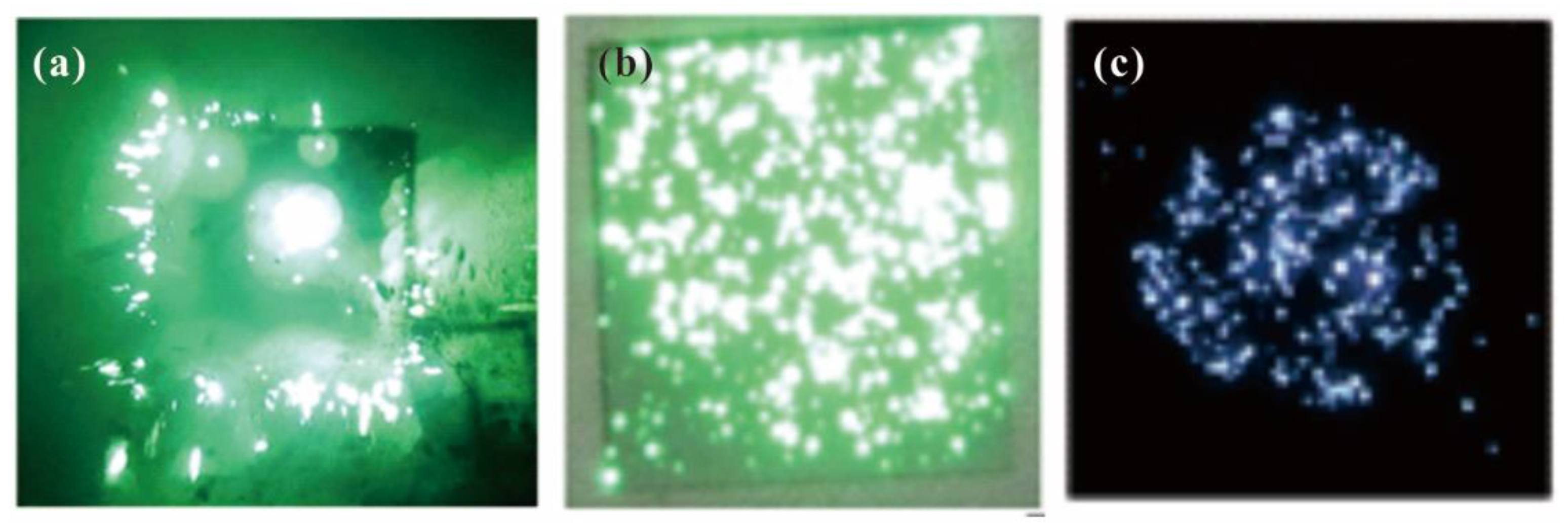
3.1. Film Measurement
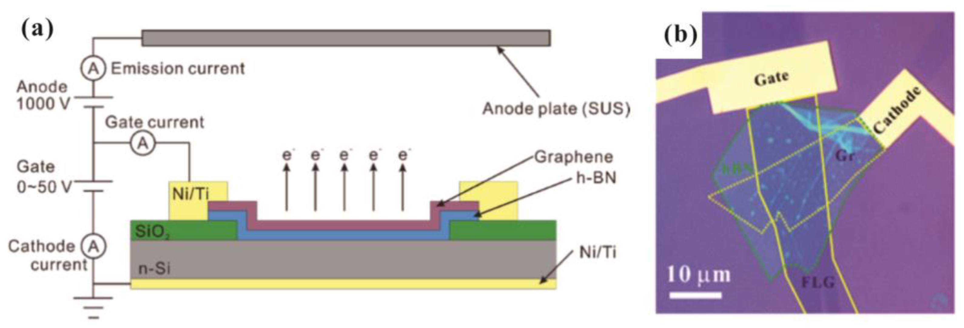
3.2. In Situ Measurement
4. Theoretical Model
4.1. Edge Emission Mode
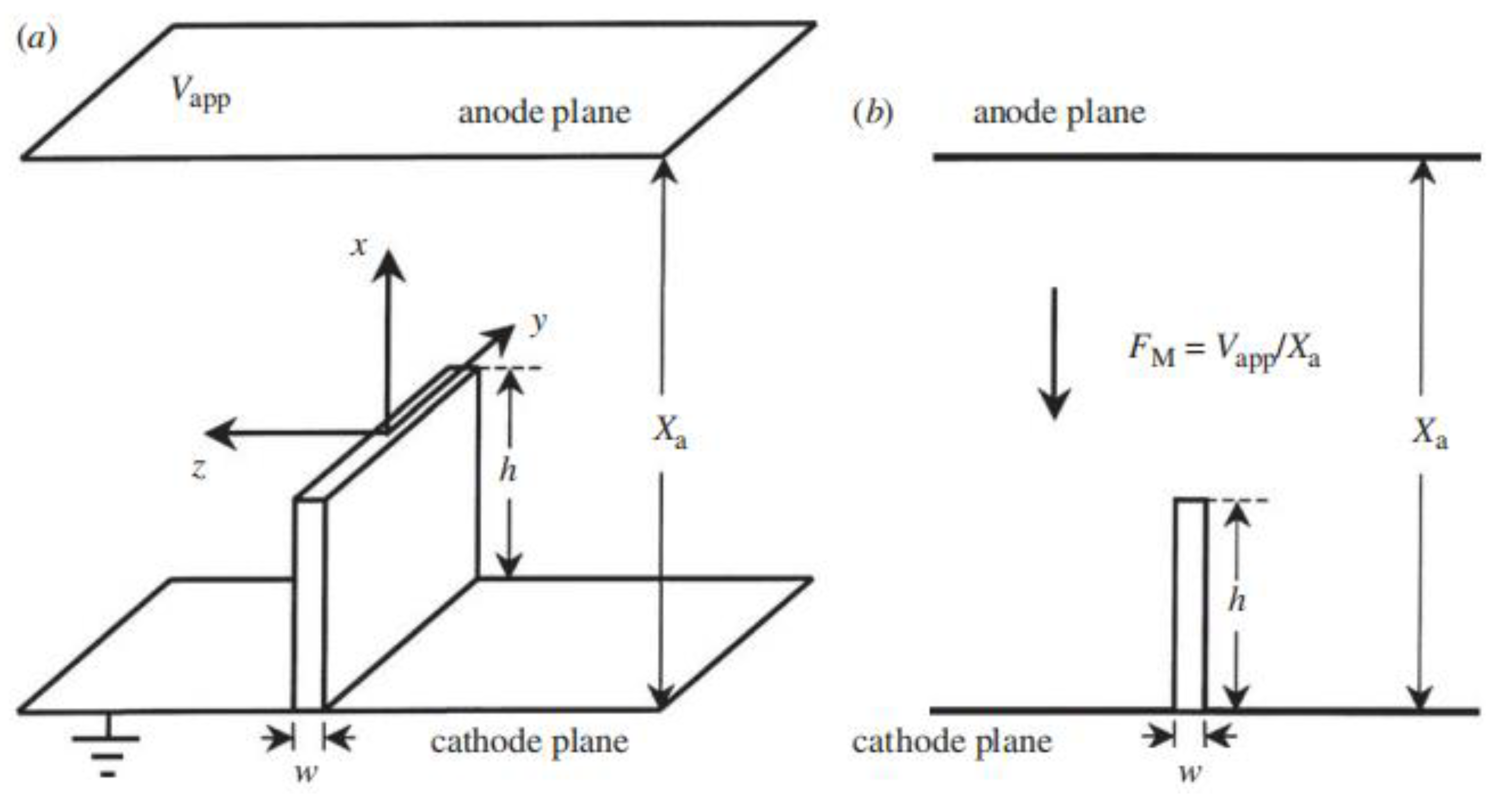
4.1.1. Classical Nanowall Model
4.1.2. Graphene Edge Emission
- (1)
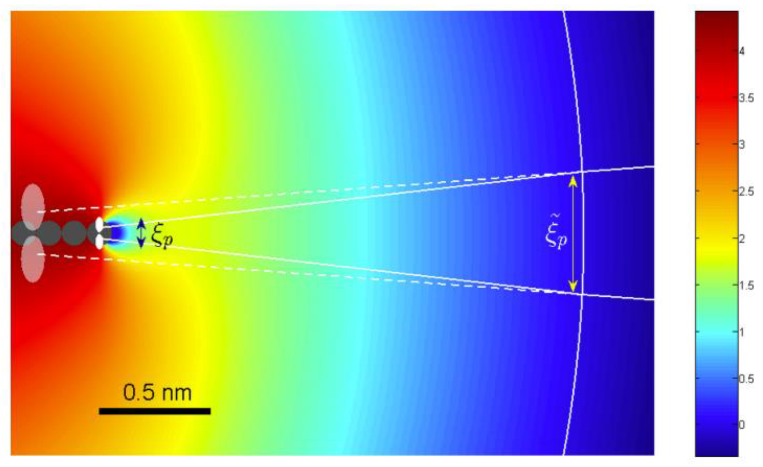
- Squeezed beamwidth
- (2)
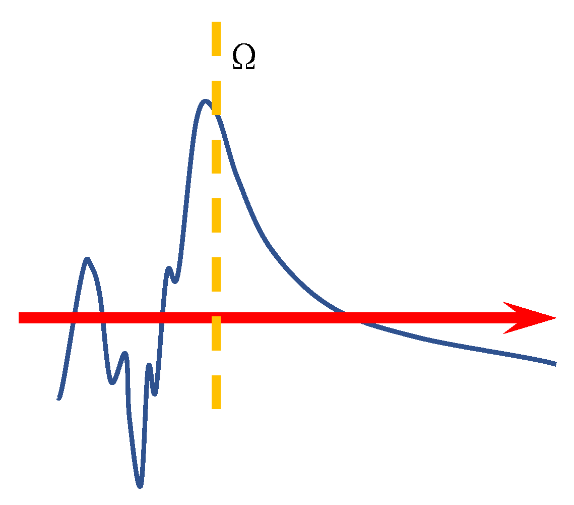
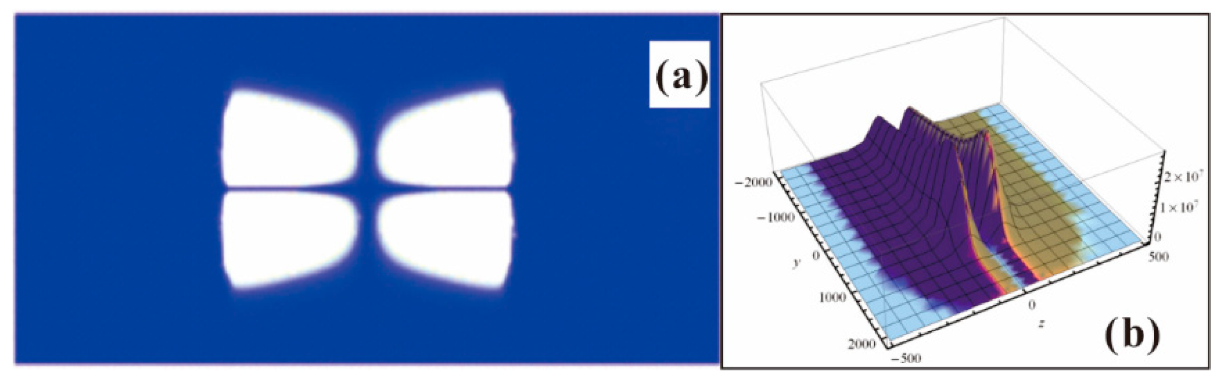
- Emission wave and interference pattern
4.2. Surface Emission Mode
4.2.1. Direct Surface Emission
4.2.2. Phonon-Assisted Surface Emission
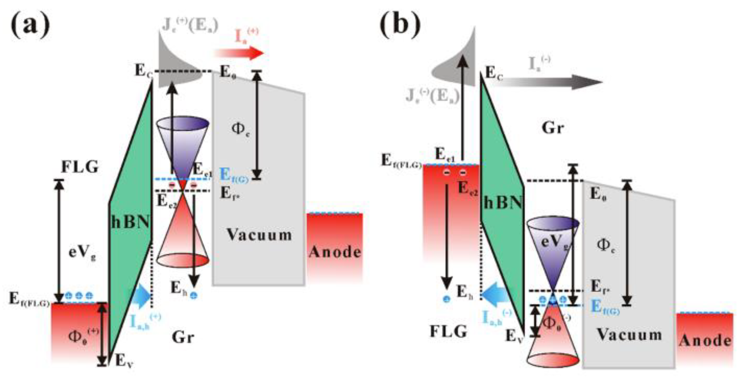
4.2.3. Auger Effect in Metal–Insulator–Graphene Heterostructure
5. Perspective
- Two-dimensional vdW materials enable cold field emitters to have more flexible structures. A close theoretical description for edge emission is possible, but the present experiments have not reached the precision to test details of the edge emission of 2D emitters, such as the angle dependency of the emission current and coherent emission patterns. Both experiments and theoretical studies find that the edge emission of 2D emitters is significantly weaker than the emission of nanotips of the same height. One simple reason is that the field enhancement factor is proportional to the square root of height/width as Equation (1), while it is of the order of height/width for 1D emitters. Considering that 2D electron systems have rich interesting physics (such as Landau levels, quantum hall effect, spin wave and valley polarization), they would be useful in the weak current applications, such as quantum state read-out and coherent single-electron sources.
- The many-body effect in 2D vdW materials needs to be further investigated because it provides an important platform for hot carrier vacuum devices. The phonon-assisted surface emission involves a complex mechanism and a precise description is still lacking. In principle, it could provide a large free-electron current. But the Joule-heat associated with the large driven current would be a bottleneck for applications. On the other hand, studies on stacked 2D cold emitters have just started. Many possible options of 2D vdW materials and their combinations would lead to novel emission properties.
- The field electron emission 2D vdW materials in either edge or surface mode are sensitive to the atomic structure of the edge/surface. Designable defects and edge/surface decorating would change the emission properties dramatically.
- The multi-field control of electron emission should have broad applications. The 2D emitters have a large surface–body ratio so they may be easier to be controlled by magnetic field or laser beam, in comparison with the solid nanotips that have a small area to receive the fields. One may think about a flexible 2D emitter that could respond to mechanical deformation.
Funding
Data Availability Statement
Conflicts of Interest
References
- Zhang, H.; Tang, J.; Yuan, J.; Yamauchi, Y.; Suzuki, T.T.; Shinya, N.; Nakajima, K.; Qin, L.-C. An ultrabright and monochromatic electron point source made of a LaB6 nanowire. Nat. Nanotech. 2016, 11, 273–280. [Google Scholar] [CrossRef] [PubMed]
- Lai, S.; Tang, X.; Liu, Y.; Mu, J.; Feng, Z.; Miao, K. X-ray high frequency pulse emission characteristic and application of CNT cold cathode X-ray source cathode X-ray source. Nanotechnology 2022, 33, 075201. [Google Scholar] [CrossRef] [PubMed]
- Yuan, X.; Zhu, W.; Zhang, Y.; Xu, N.; Yan, Y.; Wu, J.; Shen, Y.; Chen, J.; She, J.; Deng, S. A fully-sealed carbon-nanotube cold-cathode terahertz gyrotron. Sci. Rep. 2016, 6, 32936. [Google Scholar] [CrossRef] [PubMed]
- Pascale-Hamri, A.; Perisanu, S.; Derouet, A.; Journet, C.; Vincent, P.; Ayari, A.; Purcell, S.T. Ultrashort single-wall carbon nanotubes reveal field-emission coulomb blockade and highest electron-source brightness. Phys. Rev. Lett. 2014, 112, 126805. [Google Scholar] [CrossRef] [PubMed]
- Yoo, S.T.; Hong, J.H.; Kang, J.S.; Park, K.C. Deep-ultraviolet light source with a carbon nanotube cold-cathode electron beam. J. Vac. Sci. Technol. B 2018, 36, 02C103. [Google Scholar] [CrossRef]
- Shao, X.; Srinivasan, A.; Ang, W.K.; Khursheed, A. A high-brightness large-diameter graphene coated point cathode field emission electron source. Nat. Commun. 2018, 9, 1288. [Google Scholar] [CrossRef]
- Choi, W.B.; Chung, D.S.; Kang, J.H.; Kim, H.Y.; Jin, Y.W.; Han, I.T.; Lee, Y.H.; Jung, J.E.; Lee, N.S.; Park, G.S.; et al. Fully sealed, high-brightness carbon-nanotube field-emission display. Appl. Phys. Lett. 1999, 75, 3129. [Google Scholar] [CrossRef]
- Zhan, R.Z.; Chen, J.; Deng, S.Z.; Xu, N.S. Fabrication of gated CuO nanowire field emitter arrays for application in field emission display. J. Vac. Sci. Technol. B 2010, 28, 558–561. [Google Scholar] [CrossRef]
- Zheng, K.; Shen, H.; Li, J.; Sun, D.; Chen, G.; Hou, K.; Li, C.; Lei, W. The fabrication and properties of field emission display based on ZnO tetrapod-liked nanostructure. Vacuum 2009, 83, 261–264. [Google Scholar] [CrossRef]
- He, H.; She, J.C.; Huang, Y.F.; Deng, S.Z.; Xu, N.S. Precisely-controlled fabrication of single ZnO nanoemitter arrays and their possible application in low energy parallel electron beam exposure. Nanoscale 2012, 4, 2101–2108. [Google Scholar] [CrossRef]
- Nishino, H.; Yoshida, S.; Kojima, A.; Ikegami, N.; Tanaka, S.; Koshida, N.; Esashi, M. Fabrication of pierce-type nanocrystalline Si electron-emitter array for massively parallel electron beam lithography. Electr. Commun. Jpn. 2016, 99, 11–19. [Google Scholar] [CrossRef]
- Cao, X.; Zhang, G.; Zhao, Y.; Xu, Y.; She, J.; Deng, S.; Xu, N.; Chen, J. Fully vacuum-sealed addressable nanowire cold cathode flat-panel X-ray source. Appl. Phys. Lett. 2021, 119, 053501. [Google Scholar] [CrossRef]
- Chen, D.; Song, X.; Zhang, Z.; Li, Z.; She, J.; Deng, S.; Xu, N.; Chen, J. Transmission type flat-panel X-ray source using ZnO nanowire field emitters. Appl. Phys. Lett. 2015, 107, 243105. [Google Scholar]
- Chen, D.; Xu, Y.; Zhang, G.; Zhang, Z.; She, J.; Deng, S.; Xu, N.; Chen, J. A double-sided radiating flat-panel X-ray source using ZnO nanowire field emitters. Vacuum 2017, 144, 266–271. [Google Scholar] [CrossRef]
- Wang, L.; Xu, Y.; Cao, X.; Huang, J.; Deng, S.; Xu, N.; Chen, J. Diagonal 4-in ZnO nanowire cold cathode flat-panel X-ray source: Preparation and projection imaging properties. IEEE T. Nucl. Sci. 2021, 68, 338–345. [Google Scholar] [CrossRef]
- Lin, Z.; Xie, P.; Zhan, R.; Chen, D.; She, J.; Deng, S.; Xu, N.; Chen, J. Defect-enhanced field emission from WO3 nanowires for flat-panel X-ray sources. ACS Appl. Nano Mater. 2019, 2, 5206–5213. [Google Scholar]
- Posada, C.M.; Grant, E.J.; Divan, R.; Sumant, A.V.; Rosenmann, D.; Stan, L.; Lee, H.K.; Castano, C.H. Nitrogen incorporated ultrananocrystalline diamond based field emitter array for a flat-panel X-ray source. J. Appl. Phys. 2014, 115, 134506. [Google Scholar] [CrossRef]
- Zhao, Y.; Chen, Y.; Zhang, G.; Huang, D.; Zhan, R.; Deng, S.; Xu, N.; Chen, J. Pulsed voltage driving enhanced electron emission in ZnO nanowire cold cathode flat-panel X-ray source. Vacuum 2022, 199, 110970. [Google Scholar] [CrossRef]
- Novoselov, K.S.; Geim, A.K.; Morozov, S.V.; Jiang, D.; Zhang, Y.; Dubonos, S.V.; Grigorieva, I.V.; Firsov, A.A. Electric field effect in atomically thin carbon films. Science 2004, 306, 666–669. [Google Scholar] [CrossRef]
- Dwivedi, N.; Dhand, C.; Carey, J.D.; Anderson, E.C.; Kumar, R.; Srivastava, A.K.; Malik, H.K.; Saifullah, M.S.M.; Kumar, S.; Lakshminarayanan, R.; et al. The rise of carbon materials for field emission. J. Mater. Chem. C 2021, 9, 2620–2659. [Google Scholar] [CrossRef]
- Chen, Y.; Deng, S.; Xu, N.; Chen, J. Recent progress on ZnO nanowires cold cathode and its applications. Nanomaterials 2021, 11, 2150. [Google Scholar] [CrossRef] [PubMed]
- Yamaguchi, H.; Murakami, K.; Eda, G.; Fujita, T.; Guan, P.; Wang, W.; Gong, C.; Boisse, J.; Miller, S.; Acik, M.; et al. Field emission from atomically thin edges of reduced graphene oxide. ACS Nano 2011, 5, 4945–4952. [Google Scholar] [CrossRef] [PubMed]
- Wu, G.; Wei, X.; Gao, S.; Chen, Q.; Peng, L. Tunable graphene micro-emitters with fast temporal response and controllable electron emission. Nat. Commun. 2016, 7, 11513. [Google Scholar] [CrossRef] [PubMed]
- Chen, Y.; Li, Z.; Chen, J. Abnormal electron emission in a vertical graphene/hexagonal boron nitride van der Waals heterostructure driven by a hot hole induced Auger process. ACS Appl. Mater. Interfaces 2020, 12, 57505–57513. [Google Scholar] [CrossRef]
- Fowler, R.H.; Nordheim, L. Electron emission in intense electric fields. Proc. R. Soc. London. Ser. A 1928, 119, 173. [Google Scholar]
- Murphy, E.L.; Good, R.H. Thermionic emission, field emission, and the transition region. Phys. Rev. 1956, 102, 1464. [Google Scholar] [CrossRef]
- Forbes, R.G. Proposal that interpretation of field emission current–voltage characteristics should be treated as a specialized form of electrical engineering. J. Vac. Sci. Technol. B 2023, 41, 028501. [Google Scholar] [CrossRef]
- Chen, L.; Yu, H.; Zhong, J.; Wu, J.; Su, W. Graphene based hybrid/composite for electron field emission: A review. J. Alloys Compd. 2018, 749, 60–84. [Google Scholar] [CrossRef]
- Patra, A.; More, M.A.; Late, D.J.; Rout, C.S. Field emission applications of graphene analogous two dimensional materials: Recent developments and future perspectives. J. Mater. Chem. C 2021, 9, 11059–11078. [Google Scholar] [CrossRef]
- Chan, W.J.; Chua, C.; Ang, Y.S.; Ang, L.K. Field emission in emerging two-dimensional and topological materials: A perspective. IEEE Trans. Plasma Sci. 2022, 1–15. [Google Scholar] [CrossRef]
- Wu, C.; Li, F.; Zhang, Y.; Guo, T. Effectively improved field emission for graphene film by mechanical surface modification. Thin Solid Films 2013, 544, 399–402. [Google Scholar] [CrossRef]
- Suryawanshi, S.R.; More, M.A.; Late, D.J. Exfoliated 2D black phosphorus nanosheets: Field emission studies. J. Vac. Sci. Technol. B 2016, 34, 041803. [Google Scholar] [CrossRef]
- Eda, G.; Unalan, H.E.; Rupesinghe, N.; Amaratunga, G.A.J.; Chhowalla, M. Field emission from graphene based composite thin films. Appl. Phys. Lett. 2008, 93, 233502. [Google Scholar] [CrossRef]
- Wu, Z.-S.; Pei, S.; Ren, W.; Tang, D.; Gao, L.; Liu, B.; Li, F.; Liu, C.; Cheng, H.-M. Field emission of single-layer graphene films prepared by electrophoretic deposition. Adv. Mater. 2009, 21, 1756–1760. [Google Scholar] [CrossRef]
- Qian, M.; Feng, T.; Ding, H.; Lin, L.; Li, H.; Chen, Y.; Sun, Z. Electron field emission from screen-printed graphene films. Nanotechnology 2009, 20, 425702. [Google Scholar] [CrossRef]
- Kashid, R.V.; Late, D.J.; Chou, S.S.; Huang, Y.-K.; De, M.; Joag, D.S.; More, M.A.; Dravid, V.P. Enhanced field-emission behavior of layered MoS2 sheets. Small 2013, 9, 2730–2734. [Google Scholar] [CrossRef]
- Veeramalai, C.P.; Li, F.; Liu, Y.; Xu, Z.; Guo, T.; Kim, T.W. Enhanced field emission properties of molybdenum disulphide few layer nanosheets synthesized by hydrothermal method. Appl. Surf. Sci. 2016, 389, 1017–1022. [Google Scholar] [CrossRef]
- Huang, H.; Li, Y.; Li, Q.; Li, B.; Song, Z.; Huang, W.; Zhao, C.; Zhang, H.; Wen, S.; Carroll, D.; et al. Field electron emission of layered Bi2Se3 nanosheets with atom-thick sharp edges. Nanoscale 2014, 6, 8306–8310. [Google Scholar] [CrossRef]
- Huang, C.-K.; Ou, Y.; Bie, Y.; Zhao, Q.; Yu, D. Well-aligned graphene arrays for field emission displays. Appl. Phys. Lett. 2011, 98, 263104. [Google Scholar] [CrossRef]
- Malesevic, A.; Kemps, R.; Vanhulsel, A.; Chowdhury, M.P.; Volodin, A.; Haesendonck, C.V. Field emission from vertically aligned few-layer graphene. J. Appl. Phys. 2008, 104, 084301. [Google Scholar] [CrossRef]
- Zhang, Y.; Du, J.; Tang, S.; Liu, P.; Deng, S.; Chen, J.; Xu, N. Optimize the field emission character of a vertical few-layer graphene sheet by manipulating the morphology. Nanotechnology 2012, 23, 015202. [Google Scholar] [CrossRef] [PubMed]
- Zou, F.; Zhou, H.; Yu, N.; Yao, Z.; Liu, F.; Shen, C. Low-temperature controllable preparation of vertically standing graphene sheets on indium tin oxide glass and their field emission properties. Chem. Phys. Lett. 2016, 664, 29–32. [Google Scholar] [CrossRef]
- Soin, N.; Roy, S.S.; Roy, S.; Hazra, K.S.; Misra, D.S.; Lim, T.H.; Hetherington, C.J.; McLaughlin, J.A. Enhanced and stable field emission from in situ nitrogen-doped few-layered graphene nanoflakes. J. Phys. Chem. C 2011, 115, 5366–5372. [Google Scholar] [CrossRef]
- Hong, T.; Guo, C.; Zhang, Y.; Zhan, R.; Zhao, P.; Li, B.; Deng, S. Effects of substrates on nucleation, growth and electrical property of vertical few-layer graphene. Nanomaterials 2022, 12, 971. [Google Scholar] [CrossRef]
- Zhong, H.; Yang, G.; Song, H.; Liao, Q.; Cui, H.; Shen, P.; Wang, C.-X. Vertically aligned graphene-like SnS2 ultrathin nanosheet arrays: Excellent energy storage, catalysis, photoconduction, and field-emitting performance. J. Phys. Chem. C 2012, 116, 9319–9326. [Google Scholar] [CrossRef]
- Li, H.; Wu, H.; Yuan, S.; Qian, H. Synthesis and characterization of vertically standing MoS2 nanosheets. Sci. Rep. 2016, 6, 21171. [Google Scholar] [CrossRef]
- Dusane, P.R.; Thombare, B.R.; Bankar, P.K.; Lole, G.; Gavhane, D.; Khedkar, C.V.; Nagrare, B.; Salunkhe, A.; Kolhe, P.; Choudhary, R.J.; et al. Vertically aligned ultrathin MoSe2 nanoflakes grown on carbon cloth and its field emission behaviour. Mater. Res. Bull. 2019, 116, 67–71. [Google Scholar] [CrossRef]
- Kumar, M.; Park, D.Y.; Singh, R.; Jeong, M.S.; Som, T.; Kim, J. Growth of wafer-scale ReS2 with “tunable” geometry toward electron field-emission application. ACS Appl. Mater. Interfaces 2019, 11, 35845–35852. [Google Scholar] [CrossRef]
- Jadhav, C.D.; Rondiya, S.R.; Hambire, R.C.; Baviskar, D.R.; Deore, A.V.; Cross, R.W.; Dzade, N.Y.; Chavan, P.G. Highly efficient field emission properties of vertically aligned 2D CuSe nanosheets: An experimental and theoretical investigation. J. Alloys Compd. 2021, 875, 159987. [Google Scholar] [CrossRef]
- Wang, H.M.; Zheng, Z.; Wang, Y.Y.; Qiu, J.J.; Guo, Z.B.; Shen, Z.X.; Yu, T. Fabrication of graphene nanogap with crystallographically matching edges and its electron emission properties. Appl. Phys. Lett. 2010, 96, 023106. [Google Scholar] [CrossRef]
- Kumar, S.; Duesberg, G.S.; Pratap, R.; Raghavan, S. Graphene field emission devices. Appl. Phys. Lett. 2014, 105, 103107. [Google Scholar] [CrossRef]
- Shaw, J.L.; Boos, J.B.; Kong, B.D.; Robinson, J.T.; Jernigan, G.G. Field emission energy distribution and three-terminal current-voltage characteristics from planar graphene edges. J. Appl. Phys. 2019, 125, 054502. [Google Scholar] [CrossRef]
- Kleshch, V.I.; Bandurin, D.A.; Orekhov, A.S.; Purcell, S.T.; Obraztsov, A.N. Edge field emission of large-area single layer graphene. Appl. Surf. Sci. 2015, 357, 1967–1974. [Google Scholar] [CrossRef]
- Serbun, P.; Porshyn, V.; Bandurin, D.; Lützenkirchen-Hecht, D. Field emission and electron energy distributions from point-type triangular-shaped emitters made of thin graphene films. J. Appl. Phys. 2020, 127, 185302. [Google Scholar] [CrossRef]
- Gao, Y.; Okada, S. Field emission properties of edge-functionalized graphene. Carbon 2019, 142, 190–195. [Google Scholar] [CrossRef]
- Tantardini, C.; Kvashnin, A.G.; Azizi, M.; Gonze, X.; Gatti, C.; Altalhi, T.; Yakobson, B.I. Electronic properties of functionalized diamanes for field-emission displays. ACS Appl. Mater. Interfaces 2023, 15, 16317–16326. [Google Scholar] [CrossRef] [PubMed]
- Yang, Z.; Zhao, Q.; Ou, Y.; Wang, W.; Li, H.; Yua, D. Enhanced field emission from large scale uniform monolayer graphene supported by well-aligned ZnO nanowire arrays. Appl. Phys. Lett. 2012, 101, 173107. [Google Scholar] [CrossRef]
- Chang, T.; Lu, F.; Kunuku, S.; Leou, K.; Tai, N.; Lin, I. Enhanced electron field emission properties from hybrid nanostructures of graphene/Si tip array. RSC Adv. 2015, 5, 2928–2933. [Google Scholar] [CrossRef]
- Ye, D.; Moussa, S.; Ferguson, J.D.; Baski, A.A.; El-Shall, M.S. Highly efficient electron field emission from graphene oxide sheets supported by nickel nanotip arrays. Nano Lett. 2012, 12, 1265–1268. [Google Scholar] [CrossRef] [PubMed]
- Yang, T.-H.; Chiu, K.-C.; Harn, Y.-W.; Chen, H.-Y.; Cai, R.-F.; Shyue, J.-J.; Lo, S.-C.; Wu, J.-M.; Lee, Y.-H. Electron field emission of geometrically modulated monolayer semiconductors. Adv. Funct. Mater. 2018, 28, 1706113. [Google Scholar] [CrossRef]
- Yamada, T.; Masuzawa, T.; Ebisudani, T.; Okano, K.; Taniguchi, T. Field emission characteristics from graphene on hexagonal boron nitride. Appl. Phys. Lett. 2014, 104, 221603. [Google Scholar] [CrossRef]
- Murakami, K.; Igari, T.; Mitsuishi, K.; Nagao, M.; Sasaki, M.; Yamada, Y. Highly monochromatic electron emission from graphene-hexagonal boron nitride-Si heterostructure. ACS Appl. Mater. Interfaces 2020, 12, 4061–4067. [Google Scholar] [CrossRef] [PubMed]
- Murakami, K.; Miyaji, J.; Furuya, R.; Adachi, M.; Nagao, M.; Neo, Y.; Takao, Y.; Yamada, Y.; Sasaki, M.; Mimura, H. High-performance planar-type electron source based on a graphene-oxide-semiconductor structure. Appl. Phys. Lett. 2019, 114, 213501. [Google Scholar] [CrossRef]
- Murakami, K.; Tanaka, S.; Miyashita, A.; Nagao, M.; Nemoto, Y.; Masaki; Takeguchi; Fujita, J.-i. Graphene-oxide-semiconductor planar-type electron emission device. Appl. Phys. Lett. 2016, 108, 083506. [Google Scholar] [CrossRef]
- Murakami, K.; Adachi, M.; Miyaji, J.; Furuya, R.; Nagao, M.; Yamada, Y.; Neo, Y.; Takao, Y.; Sasaki, M.; Mimura, H. Mechanism of highly efficient electron emission from a graphene/oxide/semiconductor structure. ACS Appl. Electron. Mater. 2020, 2, 2265–2273. [Google Scholar] [CrossRef]
- Murakami, K.; Tanaka, S.; Iijima, T.; Nagao, M.; Nemoto, Y.; Takeguchi, M.; Yamada, Y.; Sasaki, M. Electron emission properties of graphene-oxide-semiconductor planar-type electron emission devices. J. Vac. Sci. Technol. B 2018, 36, 02C110. [Google Scholar] [CrossRef]
- Suryawanshi, S.R.; Pawbake, A.S.; Pawar, M.S.; Jadkar, S.R.; More, M.A.; Late, D.J. Enhanced field emission behavior of layered MoSe2. Mater. Res. Express 2016, 3, 035003. [Google Scholar] [CrossRef]
- Rout, C.S.; Joshi, P.D.; Kashid, R.V.; Joag, D.S.; More, M.A.; Simbeck, A.J.; Washington, M.; Nayak, S.K.; Late, D.J. Superior field emission properties of layered WS2-RGO nanocomposites. Sci. Rep. 2013, 3, 3282. [Google Scholar] [CrossRef]
- Nguyen, H.; Kang, J.S.; Li, M.; Hu, Y. High-performance field emission based on nanostructured tin selenide for nanoscale vacuum transistors. Nanoscale 2019, 11, 3129–3137. [Google Scholar] [CrossRef] [PubMed]
- Xu, N.S.; Huq, S.E. Novel cold cathode materials and applications. Mat. Sci. Eng. R 2005, 48, 47–189. [Google Scholar] [CrossRef]
- Palnitkar, U.A.; Kashid, R.V.; More, M.A.; Joag, D.S.; Panchakarla, L.S.; Rao, C.N.R. Remarkably low turn-on field emission in undoped, nitrogen-doped, and boron-doped graphene. Appl. Phys. Lett. 2010, 97, 063102. [Google Scholar] [CrossRef]
- Deng, J.-H.; Zheng, R.-T.; Zhao, Y.; Cheng, G.-A. Vapor-solid growth of few-layer graphene using radio frequency sputtering deposition and its application on field emission. ACS Nano 2012, 6, 3727–3733. [Google Scholar] [CrossRef] [PubMed]
- Stratakis, E.; Eda, G.; Yamaguchi, H.; Kymakis, E.; Fotakis, C.; Chhowalla, M. Free-standing graphene on microstructured silicon vertices for enhanced field emission properties. Nanoscale 2012, 4, 3069–3074. [Google Scholar] [CrossRef] [PubMed]
- Xiao, Z.; She, J.; Deng, S.; Tang, Z.; Li, Z.; Lu, J.; Xu, N. Field electron emission characteristics and physical mechanism of individual single-layer graphene. ACS Nano 2010, 4, 6332–6336. [Google Scholar] [CrossRef]
- Chen, J.; Cui, L.; Sun, D.; Yang, B.; Yang, J.; Yan, X. Enhanced field emission properties from aligned graphenes fabricated on micro-hole patterned stainless steel. Appl. Phys. Lett. 2014, 105, 213111. [Google Scholar] [CrossRef]
- Vadukumpully, S.; Paul, J.; Valiyaveettil, S. Cationic surfactant mediated exfoliation of graphite into graphene flakes. Carbon 2009, 47, 3288–3294. [Google Scholar] [CrossRef]
- Deng, J.-h.; Zheng, R.-t.; Yang, Y.-m.; Zhao, Y.; Cheng, G.-a. Excellent field emission characteristics from few-layer graphene–carbon nanotube hybrids synthesized using radio frequency hydrogen plasma sputtering deposition. Carbon 2012, 50, 4732–4737. [Google Scholar] [CrossRef]
- Gaur, A.P.S.; Sahoo, S.; Mendoza, F.; Rivera, A.M.; Kumar, M.; Dash, S.P.; Morell, G.; Katiyar, R.S. Cold cathode emission studies on topographically modified few layer and single layer MoS2 films. Appl. Phys. Lett. 2016, 108, 043103. [Google Scholar] [CrossRef]
- Deokar, G.; Rajput, N.S.; Li, J.; Deepak, F.L.; Ou-Yang, W.; Reckinger, N.; Bittencourt, C.; Colomer, J.-F.; Jouiad, M. Toward the use of CVD-grown MoS2 nanosheets as field-emission source. Beilstein J. Nanotechnol. 2018, 9, 1686–1694. [Google Scholar] [CrossRef]
- Bansode, S.R.; Harpale, K.V.; Mutadak, P.; Sonawane, K.M.; Chaskar, M.G.; More, M.A.; Sharma, R.B. Morphology-dependent field emission investigations from the 2-dimensional Bi2Se3-RGO nanocomposites. Mat. Sci. Eng. R 2021, 274, 115450. [Google Scholar] [CrossRef]
- Xu, J.; Wang, Q.; Tao, Z.; Qi, Z.; Zhai, Y.; Wu, S.; Zhang, X.; Lei, W. Field emission of wet transferred suspended graphene fabricated on interdigitated electrodes. ACS Appl. Mater. Interfaces 2016, 8, 3295–3300. [Google Scholar] [CrossRef] [PubMed]
- Tang, S.; Zhang, Y.; Zhao, P.; Zhan, R.; Chen, J.; Deng, S. Realizing the large current field emission characteristics of single vertical few-layer graphene by constructing a lateral graphite heat dissipation interface. Nanoscale 2021, 13, 5234. [Google Scholar] [CrossRef] [PubMed]
- Urban, F.; Passacantando, M.; Giubileo, F.; Iemmo, L.; Bartolomeo, A.D. Transport and field emission properties of MoS2 bilayers. Nanomaterials 2018, 8, 151. [Google Scholar] [CrossRef] [PubMed]
- Pelella, A.; Grillo, A.; Urban, F.; Giubileo, F.; Passacantando, M.; Pollmann, E.; Sleziona, S.; Schleberger, M.; Bartolomeo, A.D. Gate-controlled field emission current from MoS2 nanosheets. Adv. Electron. Mater. 2021, 7, 2000838. [Google Scholar] [CrossRef]
- Chen, Y.; Liu, L.; Zheng, K.; She, J.; Deng, S.; Xu, N.; Chen, J. Highly stable field emission from a tungsten diselenide monolayer on zinc oxide nanowire by geometrically modulating hot electrons. Adv. Electron. Mater. 2019, 5, 1900128. [Google Scholar] [CrossRef]
- Santandrea, S.; Giubileo, F.; Grossi, V.; Santucci, S.; Passacantando, M.; Schroeder, T.; Lupina, G.; Bartolomeo, A.D. Field emission from single and few-layer graphene flakes. Appl. Phys. Lett. 2011, 98, 163109. [Google Scholar] [CrossRef]
- Giubileo, F.; Capista, D.; Faella, E.; Pelella, A.; Kim, W.Y.; Benassi, P.; Passacantando, M.; Bartolomeo, A.D. Local characterization of field emission properties of graphene flowers. Adv. Electron. Mater. 2023, 9, 2200690. [Google Scholar] [CrossRef]
- Bartolomeo, A.D.; Urban, F.; Passacantando, M.; McEvoy, N.; Peters, L.; Iemmo, L.; Luongo, G.; Romeo, F.; Giubileo, F. A WSe2 vertical field emission transistor. Nanoscale 2019, 11, 1538–1548. [Google Scholar] [CrossRef]
- Giubileo, F.; Grillo, A.; Passacantando, M.; Urban, F.; Iemmo, L.; Luongo, G.; Pelella, A.; Loveridge, M.; Lozzi, L.; Bartolomeo, A.D. Field emission characterization of MoS2 nanoflowers. Nanomaterials 2019, 9, 717. [Google Scholar] [CrossRef]
- Iemmo, L.; Urban, F.; Giubileo, F.; Passacantando, M.; Bartolomeo, A.D. Nanotip contacts for electric transport and field emission characterization of ultrathin MoS2 flakes. Nanomaterials 2020, 10, 106. [Google Scholar] [CrossRef]
- Urban, F.; Passacantando, M.; Giubileo, F.; Iemmo, L.; Luongo, G.; Grillo, A.; Bartolomeo, A.D. Two-dimensional effects in fowler-nordheim field emission from transition metal dichalcogenides. J. Phys. Conf. Ser. 2019, 1226, 012018. [Google Scholar] [CrossRef]
- Miller, R.; Lau, Y.Y.; Booske, J.H. Electric field distribution on knife-edge field emitters. Appl. Phys. Lett. 2007, 91, 074105. [Google Scholar] [CrossRef]
- Qin, X.-Z.; Wang, W.-L.; Xu, N.-S.; Li, Z.-B.; Forbes, R.G. Analytical treatment of cold field electron emission from a nanowall emitter, including quantum confinement effects. Proc. R. Soc. A 2011, 467, 1029–1051. [Google Scholar]
- Wang, W.; Qin, X.; Xu, N.; Li, Z. Field electron emission characteristic of graphene. J. Appl. Phys. 2011, 109, 044304. [Google Scholar] [CrossRef]
- Li, Z.; Xu, N.; Kreuzer, H.J. Coherent field emission image of graphene predicted with a microscopic theory. Phys. Rev. B 2012, 85, 115427. [Google Scholar] [CrossRef]
- Luo, M.; Li, Z. Multi-field electron emission pattern of 2D emitter: Illustrated with graphene. J. Appl. Phys. 2016, 120, 204304. [Google Scholar] [CrossRef]
- Chen, J.; Li, Z.; Wang, W. Manifesting pseudo-spin polarization of graphene with field emission image. J. Appl. Phys. 2014, 115, 053701. [Google Scholar] [CrossRef]
- Wang, W.; Li, Z. Graphene with the secondary amine-terminated zigzag edge as a line electron emitter. Appl. Phys. A 2012, 109, 353–356. [Google Scholar] [CrossRef]
- Li, Z. Density functional theory for field emission from carbon nano-structures. Ultramicroscopy 2015, 159, 162–172. [Google Scholar] [CrossRef][Green Version]
- Lepetit, B. A quantum mechanical model of electron field emission from two dimensional materials. Application to graphene. J. Appl. Phys. 2021, 129, 144302. [Google Scholar] [CrossRef]
- Wei, X.; Bando, Y.; Golberg, D. Electron emission from individual graphene nanoribbons driven by internal electric field. ACS Nano 2012, 6, 705–711. [Google Scholar] [CrossRef] [PubMed]
- Wei, X.; Golberg, D.; Chen, Q.; Bando, Y.; Peng, L. Phonon-assisted electron emission from individual carbon nanotubes. Nano Lett. 2011, 11, 734–739. [Google Scholar] [CrossRef]
- Yang, W.; Li, Z.; Wang, Y.; Shen, J.; Wei, D.; Wei, X. High-performance on-chip electron sources based on electroformed silicon oxide. Adv. Electron. Mater. 2020, 6, 2000268. [Google Scholar] [CrossRef]
- Song, G.; Chen, Y.; Deng, S.; Chen, J. Improving the collection efficiency in the hot carrier tunneling device by optimizing the thickness of tunneling barrier for balancing the acceleration and scattering processes. Appl. Phys. Lett. 2023, 122, 063501. [Google Scholar] [CrossRef]
- Gerasimenko, A.Y.; Kitsyuk, E.P.; Kuksin, A.V.; Ryazanov, R.M.; Savitskiy, A.I.; Savelyev, M.S.; Pavlov, A.A. Influence of laser structuring and barium nitrate treatment on morphology and electrophysical characteristics of vertically aligned carbon nanotube arrays. Diam. Relat. Mater. 2019, 96, 104–111. [Google Scholar] [CrossRef]
- Gerasimenko, A.Y.; Kuksin, A.V.; Shaman, Y.P.; Kitsyuk, E.P.; Fedorova, Y.O.; Murashko, D.T.; Shamanaev, A.A.; Eganova, E.M.; Sysa, A.V.; Savelyev, M.S.; et al. Hybrid carbon nanotubes–graphene nanostructures: Modeling, formation, characterization. Nanomaterials 2022, 12, 2812. [Google Scholar] [CrossRef]


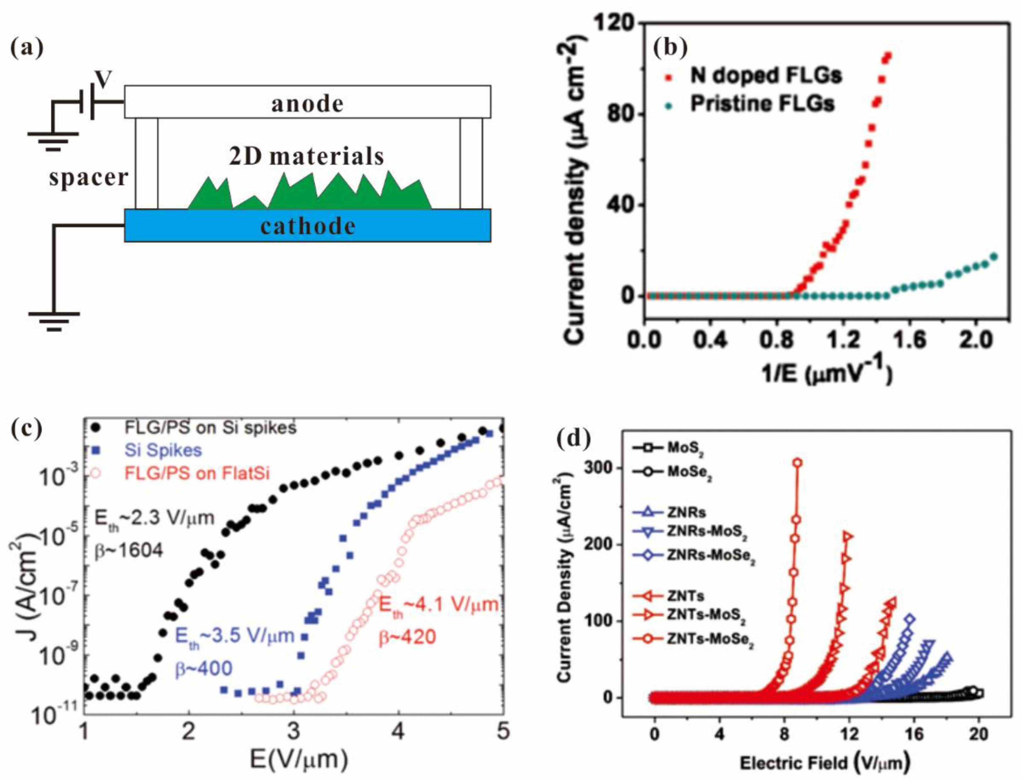
| Materials | Emitter Type | Fabrication Method | Turn-On Field (Current Density) | β | Other Field Emission Behavior |
|---|---|---|---|---|---|
| Graphene-based composite thin film | Vertical Edge emitter | Spin coating method | ~4 V/μm (10 nA/cm2) | 1200 | Nonlinear F-N plot with current saturation in the high field region was observed [33]. |
| Graphene | Vertical Edge emitter | Electrophoretic method | 2.3 V/μm | 3700 | The I-V curve followed typical F-N tunneling law [34]. |
| Vertical Edge emitter | Electrophoretic method | 4.8 V/μm (0.1 mA/cm2) | --- | The I-V curves exhibited hysteretic behavior and followed typical F-N tunneling law [75]. | |
| Vertical Edge emitter | Screen printing | 1.5 V/μm (1 μA/cm2) | 4359 | The I-V curve followed typical F-N tunneling law [35]. | |
| Vertical Edge emitter | Microfabrication technique | 7.2 V/μm (100 nA/cm2) | --- | The I-V curve followed typical F-N tunneling law [39]. | |
| Lateral Edge emitter | Microfabrication technique | --- | ~68 | The I-V curve followed Child–Langmuir law at low voltage and F-N law at high voltage [50]. | |
| Lateral Edge emitter | Mechanical cutting method | --- | --- | A strong hysteresis in current–voltage characteristics and a step-like increase in the emission current during voltage ramp up were observed [53]. | |
| Vertical Edge emitter | Adhesive tape treatment | 0.73 V/μm | 3809 | The I-V curve followed typical F-N tunneling law [31]. | |
| FLG | Vertical Edge emitter | A solution-based method | 7.5 V/μm (0.15 mA/cm2) | ~1250 | The I-V curve followed typical F-N tunneling law [76]. |
| Vertical-aligned FLG | Vertical Edge emitter | MPECVD | ~1 V/μm | ~7500 | The I-V curve followed typical F-N tunneling law [40]. |
| 1.8 V/μm | 6795 | The I-V curve followed typical F-N tunneling law [41]. | |||
| Vertical Edge emitter | PECVD | ~5 V/μm | ~1750 | The I-V curve followed typical F-N tunneling law [42]. | |
| Vertical Edge emitter | IPECVD | --- | --- | The I-V curve followed typical F-N tunneling law [44]. | |
| Vertical-aligned FLG | Vertical Edge emitter | MPECVD and N2 plasma treatment | 1.94 V/μm | 815 (low field) 4710 (high field) | Nonlinear FN plot with two linear sections in the high and low field regions was observed [43]. |
| Vertical-aligned N-doped FLG | 1 V/μm | 3120 (low field) 17,350 (high field) | |||
| N-doped graphene | Vertical Edge emitter | Arc discharge method | 0.6 V/μm | 25,849 (low field) 49,690 (high field) | Nonlinear FN plot with two linear sections in the high and low field regions was observed [71]. |
| B-doped graphene | 0.8 V/μm | 11,879 (low field) 12,067 (high field) | |||
| Graphene | 0.7 V/μm | 15,740 (low field) 24,058 (high field) | |||
| FLG on CNT | Vertical Edge emitter | Sputtering method | 0.956 V/μm | 4398 | The I-V curve followed typical F-N tunneling law [72,77]. |
| 0.98 V/μm | 3980 | ||||
| FLG on Si microspike array | Vertical Edge emitter | A solution-based method | 2.3 V/μm | 780–7300 | Nonlinear FN plot with current saturation in the high field region was observed [73]. |
| Graphene thin film | Vertical Edge emitter | Mechanical cutting method | --- | --- | Non-linear FN plot with downward bending in high field region was observed. Three discrete field emission energy peaks existed at low current and they became a single broad spectra at high current [54]. |
| Graphene/hBN/Si | Surface emitter | Transfer method | --- | --- | The I-V curve followed typical F-N tunneling law [61]. |
| Graphene on ZnO nanowire array | Surface emitter | 5.4 V/μm (1 μA/cm2) | 1100 (high field) | Nonlinear F-N plot with upward bending in the high field region was observed [57]. | |
| Graphene on Si tip | Surface emitter | 6 V/μm (---) | 1000 | The I-V curve followed typical F-N tunneling law [58]. | |
| GO on Ni nanotip array | Surface emitter | 0.5 V/μm (6.7 μA/cm2) | --- | Upward bending in high field region of the modified FN plot was observed [59]. | |
| Graphene on Ni tip | Surface emitter | CVD method | --- | --- | The I-V curve followed typical F-N tunneling law. A brightness of 1.46 × 10⁹ Am−2sr−1V−1 and energy spread of 0.246–0.42 eV were obtained [6]. |
| WS2-RGO nanocomposite | Vertical Edge emitter | Hydrothermal method | 2 V/μm (1 μA/cm2) | 2978 | Nonlinear FN plot with current saturation in high field region was observed [68]. |
| WS2 | 3.5 V/μm (1 μA/cm2) | 2468 | |||
| Few-layer MoS2 | Vertical Edge emitter | Solution-based method | 3.5 V/μm | 1138 | The I-V curve followed typical F-N tunneling law [36]. |
| Few-layer MoS2 | Vertical Edge emitter | Solution-based method | 1 V/μm (1 μA/cm2) | 9880 | The I-V curve followed typical F-N tunneling law [37]. |
| Vertical-aligned MoS2 | Vertical edge emitter | CVD method | 4.5 V/μm | ~1064 | The I-V curve followed typical F-N tunneling law [78]. |
| Vertical-aligned MoS2 | Vertical Edge emitter | CVD and transfer method | 3.1 V/μm | 856 | The I-V curve followed typical F-N tunneling law [79]. |
| Vertical-aligned MoS2 | Vertical Edge emitter | CVD method | ~2.46 V/μm | 6240 | The I-V curve followed typical F-N tunneling law [46]. |
| Vertical-aligned MoSe2 on carbon cloth | Vertical Edge emitter | Hydrothermal method | 2.4–3.68 V/μm | --- | The I-V curve followed typical F-N tunneling law [47]. |
| MoS2 | Surface emitter | A PMMA-assisted transfer method | 9.1 V/μm | --- | Three regions can be identified in the modified F-N plot [60]. |
| MoSe2 | 7.0 V/μm | --- | |||
| Bi2Se3 nanosheets | Vertical Edge emitter | Solution-based method | 2.3 V/μm | 6860 | The I-V curve followed typical F-N tunneling law [38]. |
| Bi2Se3-RGO nanocomposite | Vertical Edge emitter | Hydrothermal method | 6 V/μm (1 mA/cm2) | --- | The maximum field emission current density is 1 mA/cm2 when the field is 6 V/μm [80]. |
| Vertical-aligned few-layer ReS2 | Vertical Edge emitter | Sputtering method | 0.8 V/μm (0.6 mA/cm2) | ~3.3 ×10⁵ | The I-V curve followed typical F-N tunneling law [48]. |
| Vertical aligned SnS2 | Vertical Edge emitter | A biomolecule assisted method | 6.9 V/μm | --- | The I-V curve followed typical F-N tunneling law [45]. |
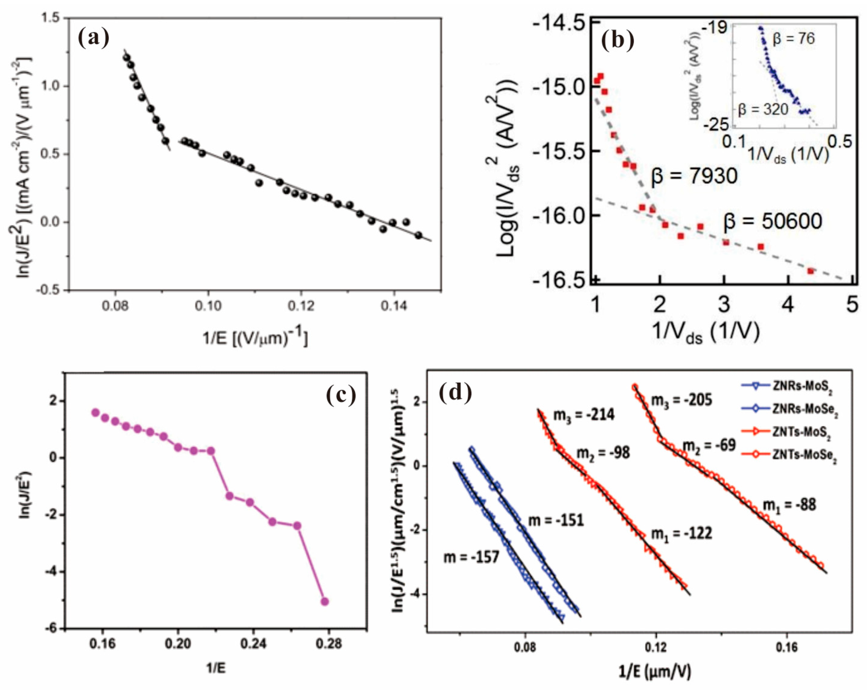
| SnSe nanoflowers | Vertical Edge emitter | Solution-based method | --- | 50,600 (low field) 7930 (high field) | Nonlinear F-N plot with upward bending in the high field region was observed [69]. |
| SnSe single crystal | Surface emitter | Mechanical exfoliation | --- | 320 (low field) 76 (high field) | |
| Few-layer BP | Vertical Edge emitter | Mechanical exfoliation | ~5.1 V/μm (~1 μA/cm2) | 1164 | The I-V curve followed typical F-N tunneling law [32]. |
| Vertical-aligned CuSe nanosheets | Vertical Edge emitter | An electrochemical method | 1.4 V/μm | 3545 | Nonlinear F-N plot with upward bending in the high field region was observed [49]. |
| Materials | Emission Mode | Remarkable Result |
|---|---|---|
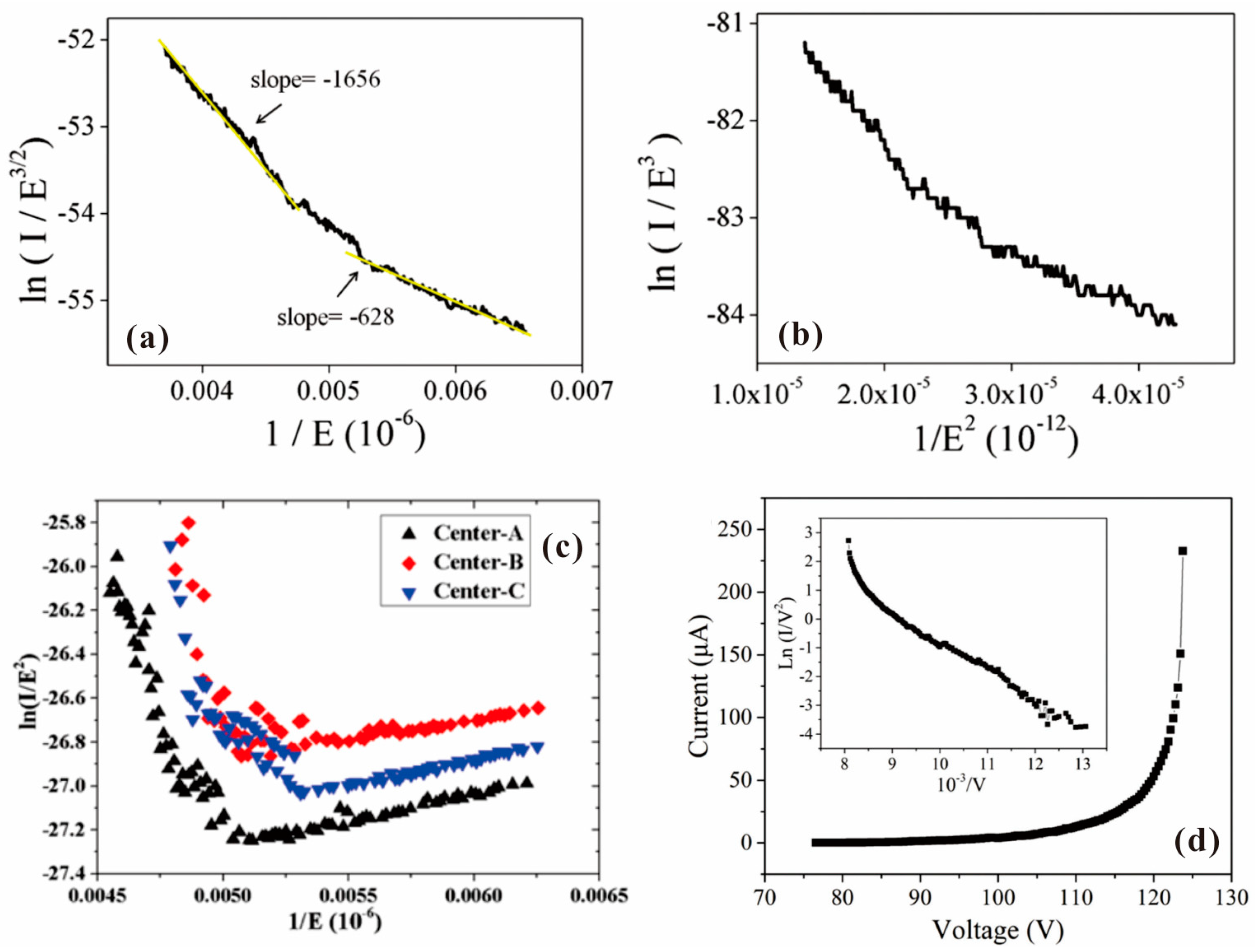
| Graphene | edge emission | Field emission I-E characteristics obey ln(I/E3/2) versus 1/E1 at high field and ln(I/E3) versus 1/E2 at low field [74]. |
| surface emission | Field emission current cannot be measured [74]. | |
| Graphene | surface emission | A transition process from space charge flow at low bias to the FN theory at high current emission regime was observed [81]. |
| Graphene | surface emission | Field emission current up to 1 μA can be measured at applied field of a few hundred volts per micrometer, which can be well described by the FN model [86]. |
| FLG | ||
| FLG nanosheets | edge emission | A turn-on field of 0.07 V/nm for a field emission current of 1 pA can be obtained [87]. |
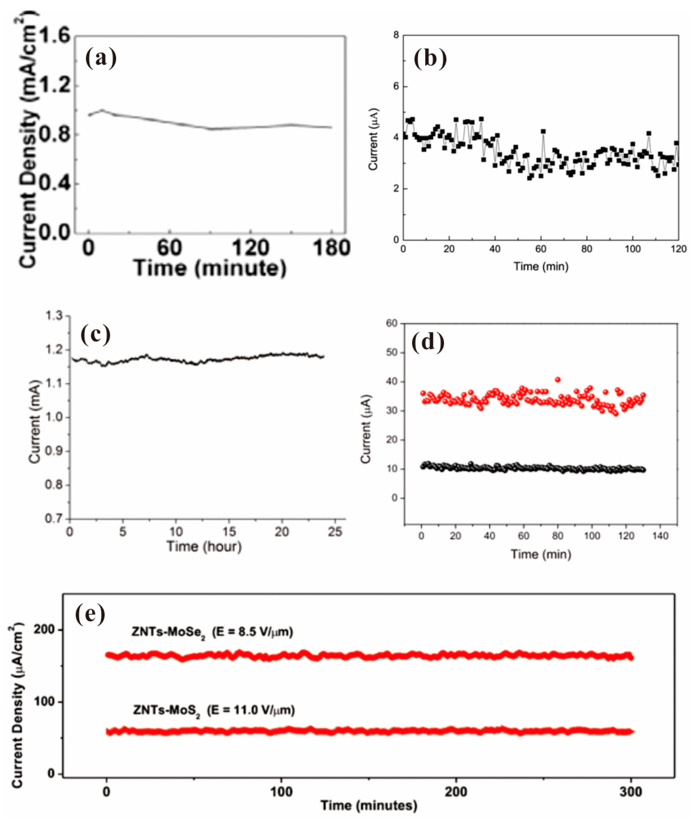
| FLG | edge emission | Single FLG with graphite interlayer helps dissipate the joule heat, which can carry a maximum current up to 233 μA [82]. |
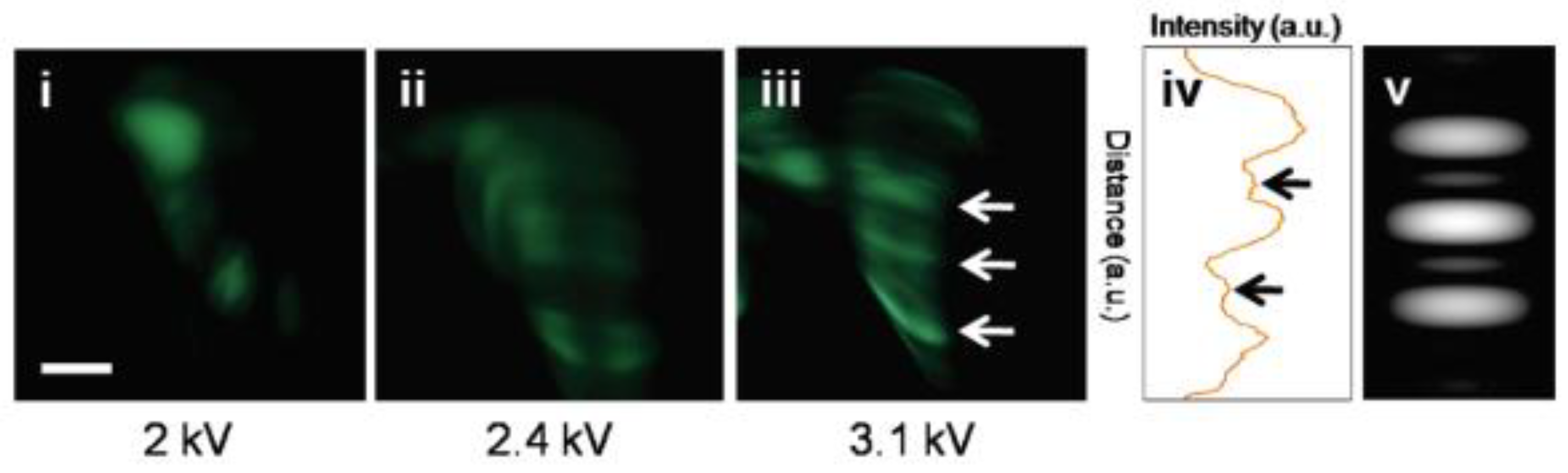
| RGO | edge emission | Field emission interference pattern from emission sites separated by a few nanometers is observed, suggesting that the emitted electrons are coherent [22]. |
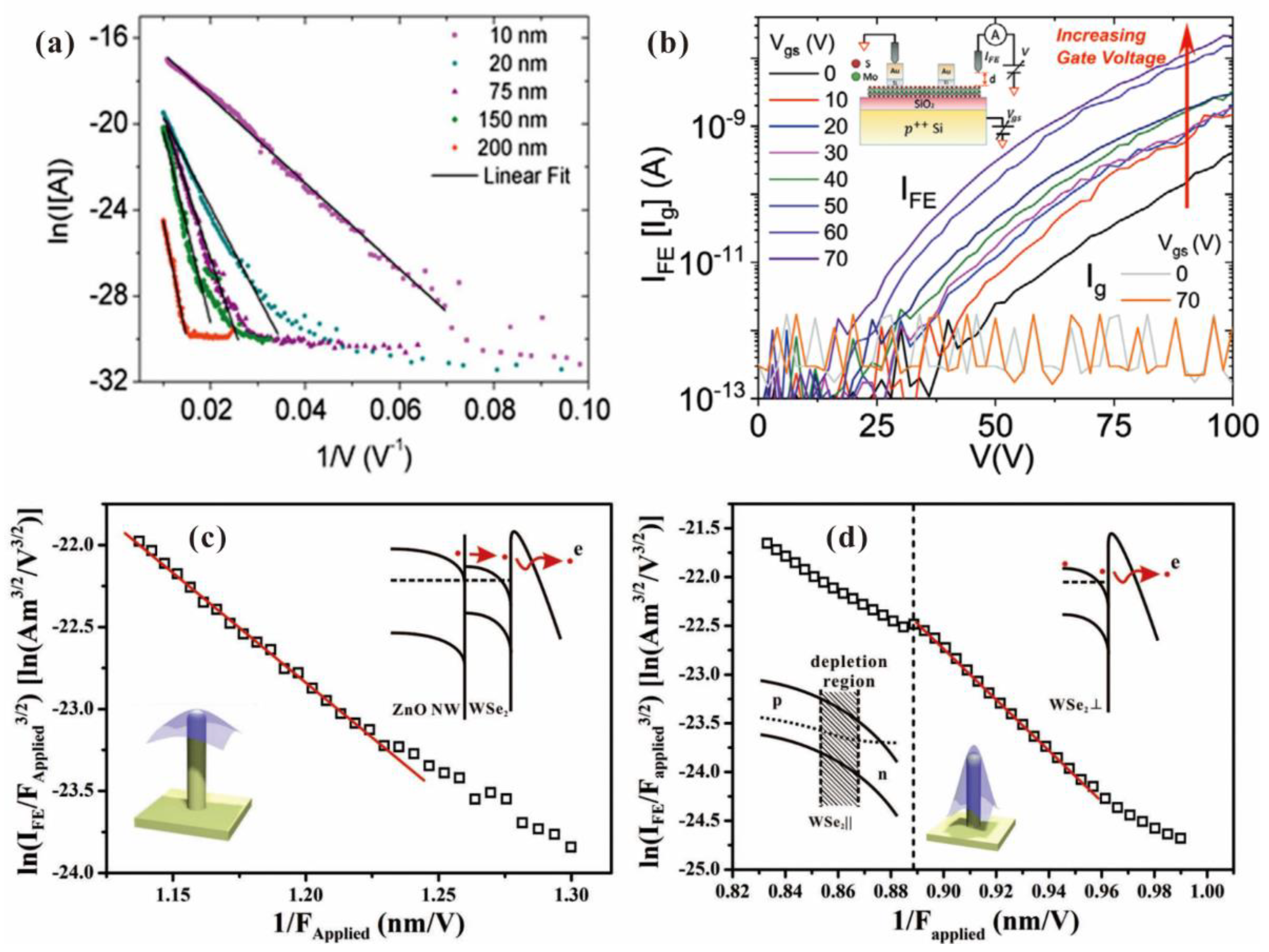
| WSe2 | surface emission | In 2D/1D hybrid structure, a “tip contact” structure is favored for achieving lower turn-on field and higher stability due to the hotter injecting electron from 1D nanostructure substrate [85]. |
| WSe2 | surface emission | The first vacuum transistor based on WSe2 monolayer was demonstrated. A turn-on field of ~100 V/μm and good stability were obtained [88]. |
| MoS2 bilayers | surface emission | Field emission current is obtained under a field of ~200 V/mm. The result obeys a modified FN model that ln(I) ∝ 1/E [83]. |
| MoS2 nanoflower | edge emission | The turn-on field decreases with the cathode–anode distance, which is inconsistent with the FN model [89]. |
| MoS2 | edge emission | Field emission current can be modulated by using a back gate structure to lower the electron affinity of MoS2, which features a new transistor based on field emission [84,90]. |
| MoS2 bilayer | surface emission | Their field emission characteristics follow a 2D modified FN model [91]. |
| WSe2 monolayer |
Disclaimer/Publisher’s Note: The statements, opinions and data contained in all publications are solely those of the individual author(s) and contributor(s) and not of MDPI and/or the editor(s). MDPI and/or the editor(s) disclaim responsibility for any injury to people or property resulting from any ideas, methods, instructions or products referred to in the content. |
© 2023 by the authors. Licensee MDPI, Basel, Switzerland. This article is an open access article distributed under the terms and conditions of the Creative Commons Attribution (CC BY) license (https://creativecommons.org/licenses/by/4.0/).
Share and Cite
Chen, Y.; Chen, J.; Li, Z. Cold Cathodes with Two-Dimensional van der Waals Materials. Nanomaterials 2023, 13, 2437. https://doi.org/10.3390/nano13172437
Chen Y, Chen J, Li Z. Cold Cathodes with Two-Dimensional van der Waals Materials. Nanomaterials. 2023; 13(17):2437. https://doi.org/10.3390/nano13172437
Chicago/Turabian StyleChen, Yicong, Jun Chen, and Zhibing Li. 2023. "Cold Cathodes with Two-Dimensional van der Waals Materials" Nanomaterials 13, no. 17: 2437. https://doi.org/10.3390/nano13172437
APA StyleChen, Y., Chen, J., & Li, Z. (2023). Cold Cathodes with Two-Dimensional van der Waals Materials. Nanomaterials, 13(17), 2437. https://doi.org/10.3390/nano13172437