
Improved Thermal Anisotropy of Multi-Layer Tungsten Telluride on Silicon Substrate

 , and
, and 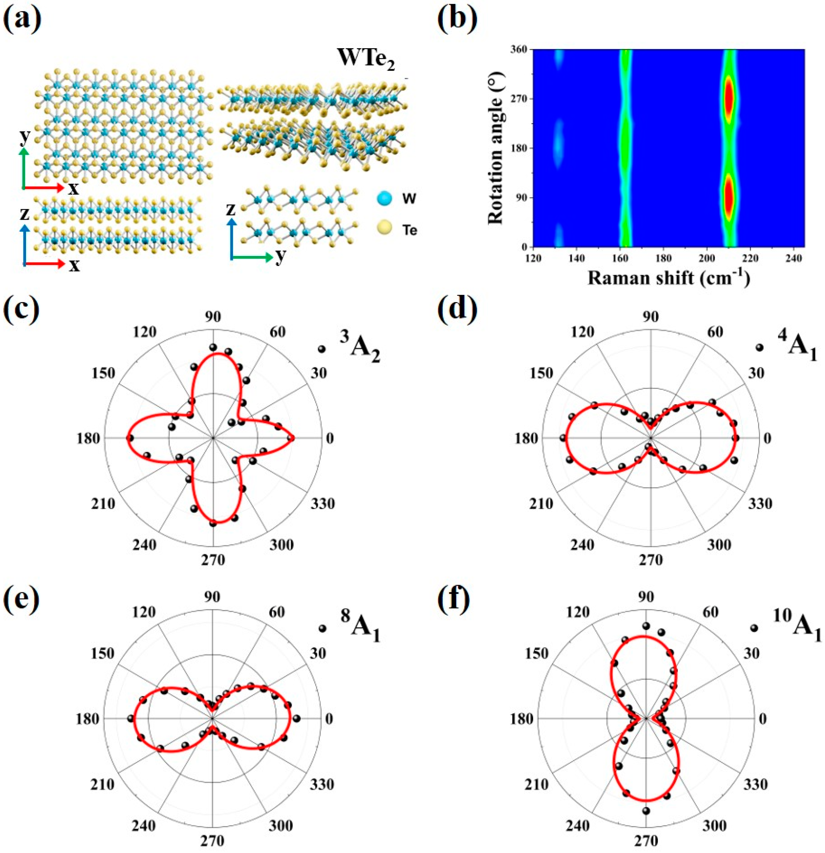
Abstract
1. Introduction
2. Materials and Methods
2.1. Preparation of WTe2 Samples
2.2. Characterizations of WTe2 Samples
2.3. Raman Thermometry Measurements of WTe2 Samples
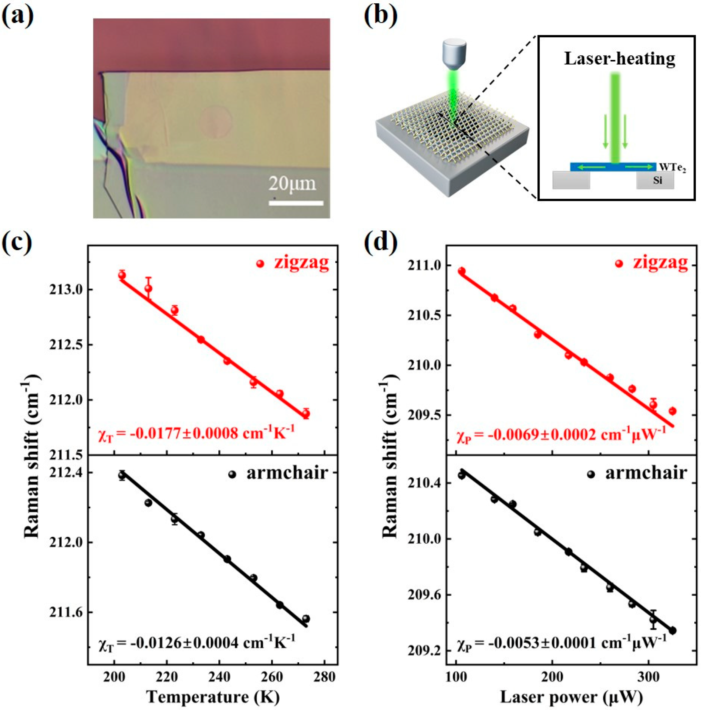
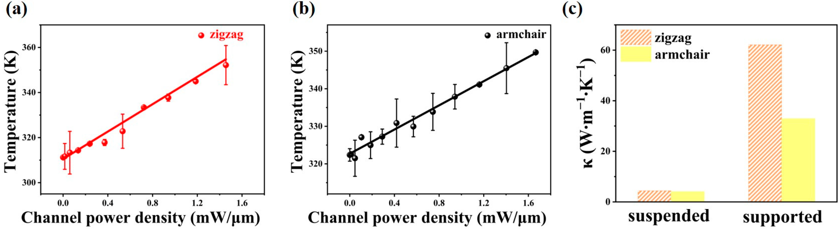
3. Results and Discussion
4. Conclusions
Supplementary Materials
Author Contributions
Funding
Institutional Review Board Statement
Informed Consent Statement
Data Availability Statement
Conflicts of Interest
References
- Ong, Z.-Y.; Cai, Y.; Zhang, G.; Zhang, Y.-W. Strong thermal transport anisotropy and strain modulation in single-layer phosphorene. J. Phys. Chem. C 2014, 118, 25272–25277. [Google Scholar] [CrossRef]
- Jain, A.; McGaughey, A.J. Strongly anisotropic in-plane thermal transport in single-layer black phosphorene. Sci. Rep. 2015, 5, 8501. [Google Scholar] [CrossRef] [PubMed]
- Luo, Z.; Maassen, J.; Deng, Y.; Du, Y.; Garrelts, R.P.; Lundstrom, M.S.; Ye, P.D.; Xu, X. Anisotropic in-plane thermal conductivity observed in few-layer black phosphorus. Nat. Commun. 2015, 6, 8572. [Google Scholar] [CrossRef]
- Xiao, P.; Chavez-Angel, E.; Chaitoglou, S.; Sledzinska, M.; Dimoulas, A.; Sotomayor Torres, C.M.; El Sachat, A. Anisotropic thermal conductivity of crystalline layered SnSe2. Nano Lett. 2021, 21, 9172–9179. [Google Scholar] [CrossRef]
- Qiu, G.; Du, Y.; Charnas, A.; Zhou, H.; Jin, S.; Luo, Z.; Zemlyanov, D.Y.; Xu, X.; Cheng, G.J.; Ye, P.D. Observation of optical and electrical in-plane anisotropy in high-mobility few-layer ZrTe5. Nano Lett. 2016, 16, 7364–7369. [Google Scholar] [CrossRef]
- Xu, X.; Song, Q.; Wang, H.; Li, P.; Zhang, K.; Wang, Y.; Yuan, K.; Yang, Z.; Ye, Y.; Dai, L. In-plane anisotropies of polarized raman response and electrical conductivity in layered tin selenide. ACS Appl. Mater. Interfaces 2017, 9, 12601–12607. [Google Scholar] [CrossRef] [PubMed]
- Wang, H.; Chen, M.-L.; Zhu, M.; Wang, Y.; Dong, B.; Sun, X.; Zhang, X.; Cao, S.; Li, X.; Huang, J. Gate tunable giant anisotropic resistance in ultra-thin GaTe. Nat. Commun. 2019, 10, 2302. [Google Scholar] [CrossRef]
- Liu, E.; Fu, Y.; Wang, Y.; Feng, Y.; Liu, H.; Wan, X.; Zhou, W.; Wang, B.; Shao, L.; Ho, C.-H. Integrated digital inverters based on two-dimensional anisotropic ReS2 field-effect transistors. Nat. Commun. 2015, 6, 6991. [Google Scholar] [CrossRef]
- Zhang, E.; Wang, P.; Li, Z.; Wang, H.; Song, C.; Huang, C.; Chen, Z.-G.; Yang, L.; Zhang, K.; Lu, S. Tunable ambipolar polarization-sensitive photodetectors based on high-anisotropy ReSe2 nanosheets. ACS Nano 2016, 10, 8067–8077. [Google Scholar] [CrossRef]
- Fei, R.; Faghaninia, A.; Soklaski, R.; Yan, J.-A.; Lo, C.; Yang, L. Enhanced thermoelectric efficiency via orthogonal electrical and thermal conductances in phosphorene. Nano Lett. 2014, 14, 6393–6399. [Google Scholar] [CrossRef]
- Das, P.; Di Sante, D.; Cilento, F.; Bigi, C.; Kopic, D.; Soranzio, D.; Sterzi, A.; Krieger, J.; Vobornik, I.; Fujii, J. Electronic properties of candidate type-II Weyl semimetal WTe2. A review perspective. Electron. Struct. 2019, 1, 014003. [Google Scholar] [CrossRef]
- Li, Y.; Liu, J.; Zhang, P.; Zhang, J.; Xiao, N.; Yu, L.; Niu, P. Electrical transport properties of Weyl semimetal WTe2 under high pressure. J. Mater. Sci. 2020, 55, 14873–14882. [Google Scholar] [CrossRef]
- Homes, C.; Ali, M.; Cava, R.J. Optical properties of the perfectly compensated semimetal WTe2. Phys. Rev. B 2015, 92, 161109. [Google Scholar] [CrossRef]
- Chen, Y.; Deng, C.; Wei, Y.; Liu, J.; Su, Y.; Xie, S.; Cai, W.; Peng, G.; Huang, H.; Dai, M. Thickness dependent anisotropy of in-plane Raman modes under different temperatures in supported few-layer WTe2. Appl. Phys. Lett. 2021, 119, 063104. [Google Scholar] [CrossRef]
- Pan, X.-C.; Chen, X.; Liu, H.; Feng, Y.; Wei, Z.; Zhou, Y.; Chi, Z.; Pi, L.; Yen, F.; Song, F. Pressure-driven dome-shaped superconductivity and electronic structural evolution in tungsten ditelluride. Nat. Commun. 2015, 6, 7805. [Google Scholar] [CrossRef]
- Kang, D.; Zhou, Y.; Yi, W.; Yang, C.; Guo, J.; Shi, Y.; Zhang, S.; Wang, Z.; Zhang, C.; Jiang, S. Superconductivity emerging from a suppressed large magnetoresistant state in tungsten ditelluride. Nat. Commun. 2015, 6, 7804. [Google Scholar] [CrossRef]
- Zhang, Q.; Zhang, R.; Chen, J.; Shen, W.; An, C.; Hu, X.; Dong, M.; Liu, J.; Zhu, L. Remarkable electronic and optical anisotropy of layered 1T’-WTe2 2D materials. Beilstein J. Nanotechnol. 2019, 10, 1745–1753. [Google Scholar] [CrossRef]
- Wang, Q.; Yesilyurt, C.; Liu, F.; Siu, Z.B.; Cai, K.; Kumar, D.; Liu, Z.; Jalil, M.B.; Yang, H. Anomalous photothermoelectric transport due to anisotropic energy dispersion in WTe2. Nano Lett. 2019, 19, 2647–2652. [Google Scholar] [CrossRef]
- Jha, R.; Onishi, S.; Higashinaka, R.; Matsuda, T.D.; Ribeiro, R.A.; Aoki, Y. Anisotropy in the electronic transport properties of Weyl semimetal WTe2 single crystals. AIP Adv. 2018, 8, 101332. [Google Scholar] [CrossRef]
- Zhou, W.; Chen, J.; Gao, H.; Hu, T.; Ruan, S.; Stroppa, A.; Ren, W. Anomalous and Polarization-Sensitive Photoresponse of Td-WTe2 from Visible to Infrared Light. Adv. Mater. 2019, 31, 1804629. [Google Scholar] [CrossRef]
- Torun, E.; Sahin, H.; Cahangirov, S.; Rubio, A.; Peeters, F. Anisotropic electronic, mechanical, and optical properties of monolayer WTe2. J. Appl. Phys. 2016, 119, 074307. [Google Scholar] [CrossRef]
- Xu, Z.; Luo, B.; Chen, Y.; Li, X.; Chen, Z.; Yuan, Q.; Xiao, X. High sensitivity and anisotropic broadband photoresponse of Td-WTe2. Phys. Lett. A 2021, 389, 127093. [Google Scholar] [CrossRef]
- Chen, X.-K.; Hu, X.-Y.; Jia, P.; Xie, Z.-X.; Liu, J. Tunable anisotropic thermal transport in porous carbon foams: The role of phonon coupling. Int. J. Mech. Sci. 2021, 206, 106576. [Google Scholar] [CrossRef]
- Liu, X.; Zhang, G.; Zhang, Y.-W. Surface-engineered nanoscale diamond films enable remarkable enhancement in thermal conductivity and anisotropy. Carbon 2015, 94, 760–767. [Google Scholar] [CrossRef]
- Qin, G.; Yan, Q.-B.; Qin, Z.; Yue, S.-Y.; Hu, M.; Su, G. Anisotropic intrinsic lattice thermal conductivity of phosphorene from first principles. Phys. Chem. Chem. Phys. 2015, 17, 4854–4858. [Google Scholar] [CrossRef]
- Liu, T.-H.; Chang, C.-C. Anisotropic thermal transport in phosphorene: Effects of crystal orientation. Nanoscale 2015, 7, 10648–10654. [Google Scholar] [CrossRef]
- Chen, J.; Chen, S.; Gao, Y. Anisotropy enhancement of thermal energy transport in supported black phosphorene. J. Phys. Chem. Lett. 2016, 7, 2518–2523. [Google Scholar] [CrossRef] [PubMed]
- Chen, Y.; Peng, B.; Cong, C.; Shang, J.; Wu, L.; Yang, W.; Zhou, J.; Yu, P.; Zhang, H.; Wang, Y. In-Plane Anisotropic Thermal Conductivity of Few-Layered Transition Metal Dichalcogenide Td-WTe2. Adv. Mater. 2019, 31, 1804979. [Google Scholar] [CrossRef] [PubMed]
- Bormashenko, E.; Pogreb, R.; Sutovsky, S.; Lusternik, V.; Voronel, A. Mechanical and thermodynamic properties of infrared transparent low melting chalcogenide glass. Infrared Phys. Technol. 2002, 43, 397–399. [Google Scholar] [CrossRef]
- Zhang, X.; Tan, Q.-H.; Wu, J.-B.; Shi, W.; Tan, P.-H. Review on the Raman spectroscopy of different types of layered materials. Nanoscale 2016, 8, 6435–6450. [Google Scholar] [CrossRef] [PubMed]
- Wu, J.B.; Zhao, H.; Li, Y.; Ohlberg, D.; Shi, W.; Wu, W.; Wang, H.; Tan, P.H. Monolayer molybdenum disulfide nanoribbons with high optical anisotropy. Adv. Opt. Mater. 2016, 4, 756–762. [Google Scholar] [CrossRef]
- Wu, J.-B.; Lin, M.-L.; Cong, X.; Liu, H.-N.; Tan, P.-H. Raman spectroscopy of graphene-based materials and its applications in related devices. Chem. Soc. Rev. 2018, 47, 1822–1873. [Google Scholar] [CrossRef]
- Song, Q.; Pan, X.; Wang, H.; Zhang, K.; Tan, Q.; Li, P.; Wan, Y.; Wang, Y.; Xu, X.; Lin, M. The in-plane anisotropy of WTe2 investigated by angle-dependent and polarized Raman spectroscopy. Sci. Rep. 2016, 6, 29254. [Google Scholar] [CrossRef]
- Zhou, Z.; Cui, Y.; Tan, P.-H.; Liu, X.; Wei, Z. Optical and electrical properties of two-dimensional anisotropic materials. J. Semicond. 2019, 40, 061001. [Google Scholar] [CrossRef]
- Ribeiro, H.B.; Pimenta, M.A.; De Matos, C.J.; Moreira, R.L.; Rodin, A.S.; Zapata, J.D.; De Souza, E.A.; Castro Neto, A.H. Unusual angular dependence of the Raman response in black phosphorus. ACS Nano 2015, 9, 4270–4276. [Google Scholar] [CrossRef] [PubMed]
- Balandin, A.A.; Ghosh, S.; Bao, W.; Calizo, I.; Teweldebrhan, D.; Miao, F.; Lau, C.N. Superior thermal conductivity of single-layer graphene. Nano Lett. 2008, 8, 902–907. [Google Scholar] [CrossRef] [PubMed]
- Yan, R.; Simpson, J.R.; Bertolazzi, S.; Brivio, J.; Watson, M.; Wu, X.; Kis, A.; Luo, T.; Hight Walker, A.R.; Xing, H.G. Thermal conductivity of monolayer molybdenum disulfide obtained from temperature-dependent Raman spectroscopy. ACS Nano 2014, 8, 986–993. [Google Scholar] [CrossRef] [PubMed]
- Peimyoo, N.; Shang, J.; Yang, W.; Wang, Y.; Cong, C.; Yu, T. Thermal conductivity determination of suspended mono-and bilayer WS2 by Raman spectroscopy. Nano Res. 2015, 8, 1210–1221. [Google Scholar] [CrossRef]
- Chen, C.-C.; Li, Z.; Shi, L.; Cronin, S.B. Thermal interface conductance across a graphene/hexagonal boron nitride heterojunction. Appl. Phys. Lett. 2014, 104, 081908. [Google Scholar] [CrossRef]
- Wei, Y.; Deng, C.; Zheng, X.; Chen, Y.; Zhang, X.; Luo, W.; Zhang, Y.; Peng, G.; Liu, J.; Huang, H. Anisotropic in-plane thermal conductivity for multi-layer WTe2. Nano Res. 2022, 15, 401–407. [Google Scholar] [CrossRef]
- Su, Y.; Deng, C.; Liu, J.; Zheng, X.; Wei, Y.; Chen, Y.; Yu, W.; Guo, X.; Cai, W.; Peng, G. Highly in-plane anisotropy of thermal transport in suspended ternary chalcogenide Ta2NiS5. Nano Res. 2022, 15, 6601–6606. [Google Scholar] [CrossRef]
- Liu, X.-L.; Zhang, X.; Lin, M.-L.; Tan, P.-H. Different angle-resolved polarization configurations of Raman spectroscopy: A case on the basal and edge plane of two-dimensional materials. Chin. Phys. B 2017, 26, 067802. [Google Scholar] [CrossRef]
- Loudon, R. The Raman effect in crystals. Adv. Phys. 2001, 50, 813–864. [Google Scholar] [CrossRef]
- Jana, M.K.; Singh, A.; Late, D.J.; Rajamathi, C.R.; Biswas, K.; Felser, C.; Waghmare, U.V.; Rao, C. A combined experimental and theoretical study of the structural, electronic and vibrational properties of bulk and few-layer Td-WTe2. J. Phys. Condens. Matter 2015, 27, 285401. [Google Scholar] [CrossRef] [PubMed]
- Calizo, I.; Balandin, A.; Bao, W.; Miao, F.; Lau, C. Temperature dependence of the Raman spectra of graphene and graphene multilayers. Nano Lett. 2007, 7, 2645–2649. [Google Scholar] [CrossRef] [PubMed]
- Vaziri, S.; Yalon, E.; Muñoz Rojo, M.; Suryavanshi, S.V.; Zhang, H.; McClellan, C.J.; Bailey, C.S.; Smithe, K.K.; Gabourie, A.J.; Chen, V. Ultrahigh thermal isolation across heterogeneously layered two-dimensional materials. Sci. Adv. 2019, 5, eaax1325. [Google Scholar] [CrossRef]
- Ma, J.; Chen, Y.; Han, Z.; Li, W. Strong anisotropic thermal conductivity of monolayer WTe2. 2D Mater. 2016, 3, 045010. [Google Scholar] [CrossRef]
- Laxmi, V.; Basu, N.; Nayak, P.K. Substrate dependent thermal conductivity in Td-WTe2 using micro-Raman spectroscopy. J. Raman Spectrosc. 2023, 54, 76–83. [Google Scholar] [CrossRef]


Disclaimer/Publisher’s Note: The statements, opinions and data contained in all publications are solely those of the individual author(s) and contributor(s) and not of MDPI and/or the editor(s). MDPI and/or the editor(s) disclaim responsibility for any injury to people or property resulting from any ideas, methods, instructions or products referred to in the content. |
© 2023 by the authors. Licensee MDPI, Basel, Switzerland. This article is an open access article distributed under the terms and conditions of the Creative Commons Attribution (CC BY) license (https://creativecommons.org/licenses/by/4.0/).
Share and Cite
Fang, M.; Liu, X.; Liu, J.; Chen, Y.; Su, Y.; Wei, Y.; Zhou, Y.; Peng, G.; Cai, W.; Deng, C.; et al. Improved Thermal Anisotropy of Multi-Layer Tungsten Telluride on Silicon Substrate. Nanomaterials 2023, 13, 1817. https://doi.org/10.3390/nano13121817
Fang M, Liu X, Liu J, Chen Y, Su Y, Wei Y, Zhou Y, Peng G, Cai W, Deng C, et al. Improved Thermal Anisotropy of Multi-Layer Tungsten Telluride on Silicon Substrate. Nanomaterials. 2023; 13(12):1817. https://doi.org/10.3390/nano13121817
Chicago/Turabian StyleFang, Mengke, Xiao Liu, Jinxin Liu, Yangbo Chen, Yue Su, Yuehua Wei, Yuquan Zhou, Gang Peng, Weiwei Cai, Chuyun Deng, and et al. 2023. "Improved Thermal Anisotropy of Multi-Layer Tungsten Telluride on Silicon Substrate" Nanomaterials 13, no. 12: 1817. https://doi.org/10.3390/nano13121817
APA StyleFang, M., Liu, X., Liu, J., Chen, Y., Su, Y., Wei, Y., Zhou, Y., Peng, G., Cai, W., Deng, C., & Zhang, X.-A. (2023). Improved Thermal Anisotropy of Multi-Layer Tungsten Telluride on Silicon Substrate. Nanomaterials, 13(12), 1817. https://doi.org/10.3390/nano13121817