1. Introduction
Utilizing renewable resources and energy is the sole source for the exponential increase in the energy demand and climate crisis. Solar energy is one of the most generous renewable resources on the earth [
1]. From the last decade, hybrid perovskites have gained an immense attraction within the field of solar cells due to significant growth in its power conversion efficiency (PCE), and is generally considered as an upcoming advance in solar cells [
2,
3]. Furthermore, its excellent photovoltaic (PV) performance and economical in nature [
4,
5] has drawn researchers toward it. Properties like high optical absorption coefficient value, defect-tolerant properties, long carrier lifetime and diffusion length (>1 µm for perovskite), flat, broad absorption at shorter wavelength and due to the development of roll-to-roll technology make them a promising candidate for visible light optoelectronics at a large scale [
2,
6]. Perovskite solar cells (PSCs), as compared to others, are very reliable, being cost effective and having an efficiency of PSCs (25.2%) close to Si-solar cells (26.1%) with an expectation of nearly 28% in the near future [
6]. Escalating the PCE by adopting different routes such as interface modification, or compositional engineering such as doping engineering and morphology alteration are the key research focus [
7,
8], as with minimizing the non-radiative energy loss at the interface of the photoactive layer and transport layer. The photovoltaic performance of the perovskite also depends on the reduction in parasitic absorption in the interlayers and at the metal contact [
9].
However, the efficiency of single-junction cells is difficult to break through, and it cannot provide enough solar power, so it is a costly deal as compared to thermal power generation. Multi-junction solar cells are expected to solve this problem. Many researchers have combined materials with different energy gaps through tandem technology to achieve a multiplicative effect. Since perovskite materials have the capability of energy gap tuning in the range of 1.51–2.18 eV by changing the halide in their structure, they can be applied to many tandem solar cell architectures (i.e., top cell or bottom sub cell), with inorganic or organic secondary cells, even combined with photoelectrochemical cells. Taking the double-junction solar cell as an example, it has a theoretical efficiency of around 43% [
10], and the efficiency of group III–V semiconductors is the highest. However, due to the complicated epitaxial process, the cost is relatively high, and the application range cannot be as wide as that of a silicon solar cell. Therefore, research is on how to combine other solar cells, so that these two materials work together and complement each other. Among the various combinations of semiconductors for perovskite, perovskite/silicon (PSC/Si) is the most common tandem cell combination, mainly as silicon crystalline solar cells are easy to obtain and the power generation performance is quite stable. A Perovskite–Si hybrid structure for solar cells has great potential for large-scale industrial production. Perovskite mainly converts green light and blue light into electricity, while silicon is responsible for red light and near-infrared light, making excellent use of the solar spectrum. Therefore, high band-gap perovskites are important materials and are preferred for multi-junction solar cell architectures.
Generally, MAPbI
xCl
3−x has higher bandgap energy with excellent optoelectronic properties as compared to MAPbI
3. Doping engineering like the addition of halogen atoms to chlorine (Cl
−) in CH
3NH
3I
3 resulting in CH
3NH
3I
xCl
3−x also enhances the stability and carrier mobility. To date, various methods like solution process using one-step or two-step solution process spin-coating for active layer and vapor deposition technique are widely adopted for the fabrication of the composite [
11,
12]. Controlling the growth rate of crystallization in a traditional one-step or two step solution process is very difficult, limiting the production of CH
3NH
3I
xCl
3−x at a large scale. Recently, thermal evaporation has been widely accepted for the large-scale production of various perovskite solar cells. Poor crystallinity, and the effect of a different evaporation rate for the perovskite, leading to residual formation, are some of the major issues experienced when using thermal evaporation, limiting the commercialization [
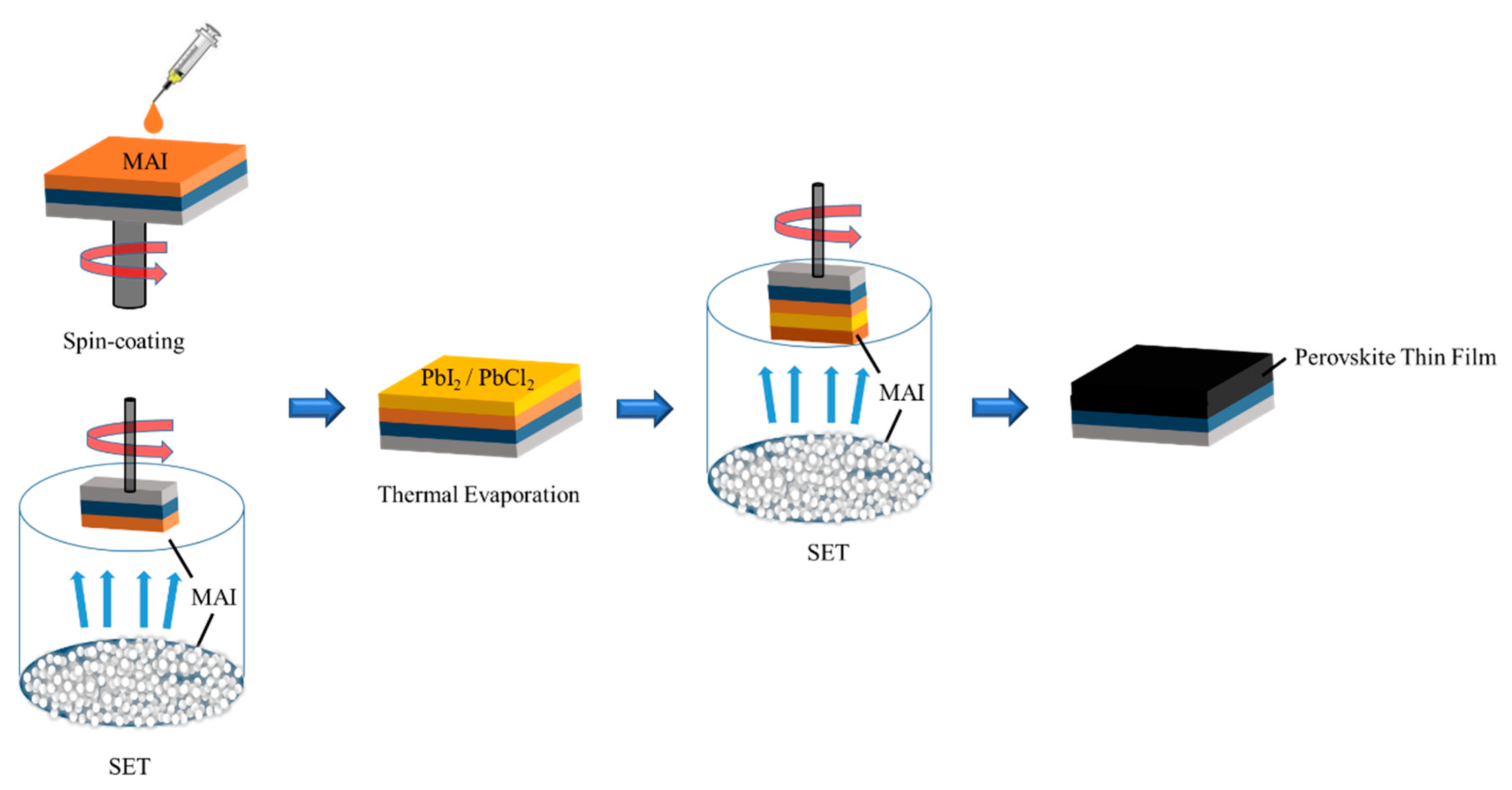
13]. In this article, solving the issue faced from a traditional evaporation technique, double-sided sandwich evaporation technique (DS-SET) was adopted using a low-cost homemade chamber for the all-evaporated perovskite. The proposed sandwich structure comprises of MAI-PbI
2-MAI and MAI-PbCl
2-MAI, with methylammonium iodide (MAI) as the bottom layer formed via spin-coating or a homemade sandwich evaporation technique (SET) chamber, further with the evaporation of PbCl
2 or PbI
2 using an evaporator, and then layering the MAI powder as the top layer with the same SET setup, respectively. The so-formed MAPbI
3 perovskite showed a PCE (%) of 14.8%, whereas, MAPbI
xCl
3−x has a PCE (%) of 16.25% and the longer diffusion length of the latter is responsible for the higher PCE. The crystallinity was also enhanced to a great extent by using this technique for the perovskite fabrication.
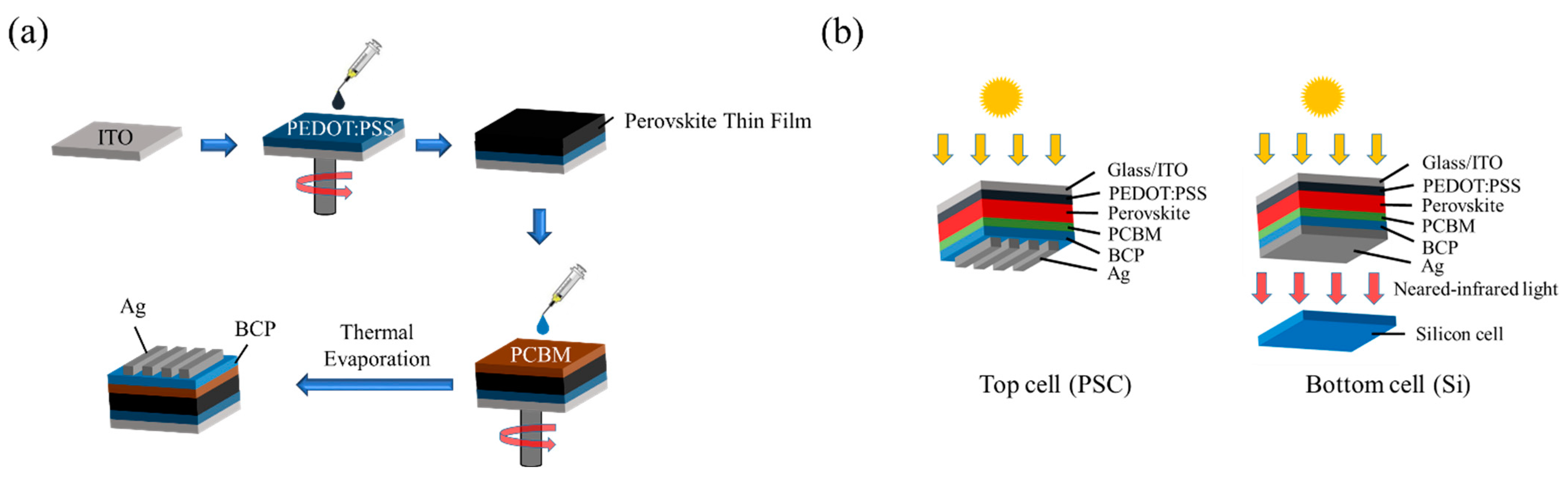
Besides, the top solar cell must transmit the light so that the bottom solar cell can absorb the corresponding spectrum. Transparent electrode transmittance affects the absorption range and absorption rate of the bottom cell. Therefore, PSCs with transparent electrodes are crucial for the performance of silicon solar cells as the bottom cell. Thereupon, we investigated an efficient transparent electrode with better conductivity, high transmittance and found that the use of a thermally evaporated silver thin film as the transparent electrodes with further post-annealing can effectively solve the problems related to transmittance, conductivity, and damage to the perovskite film during the manufacturing process [
14].
Usually, the two secondary cells of the four terminals (4T) are fabricated on separate substrates, with the two operating independently, and are stacked on the top of each other. The 4T does not consider the matching of the upper and lower cell currents, which has the advantage of a simple structure. Therefore, PSC is combined with the silicon solar cell through a 4T configuration to form a tandem solar cell in this work. Using the DS-SET method, we produced the chlorine-based perovskite solar cell combined with a transparent electrode with PCE, a fill factor of the top-cell of 16.1% and 74.25%, respectively, along with PCE, a fill factor of the bottom cell of 8.33% and 75.54%, respectively, resulting in a high PCE of 24.43%.
3. Results and Discussion
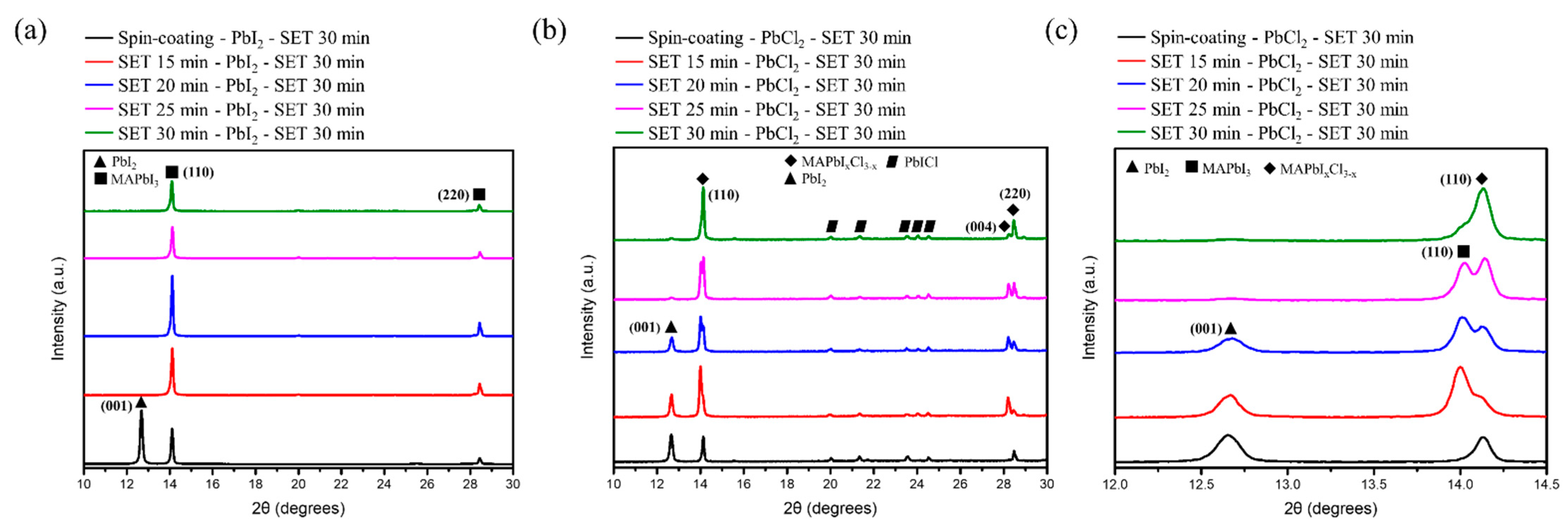
In order to realize the formation and evolution of the perovskite thin film phase and crystallization by the variation in fabrication technique, XRD analysis was performed. The strength of the ionic bond Pb-X (X = Cl, I) generates strain energy due to the size mismatch between the two different halides and plays an important role in the physical properties of perovskite films. From the periodic table, compared to an I
− ion, Cl
− has higher electronegativity, which results in a stronger bond formation with Pb
2+, and these stronger ionic bond help to overcome the strain energy that evolves from the lattice size mismatch. From the unit cell volume for MAPbI
3 and MAPbI
xCl
3−x calculation, it clearly depicts that there is a reduction in the unit cell volume from MAPbI
3 to MAPbI
xCl
3−x for the same SET time, indicating that the successful incorporation of Cl
− and anion mixing in the sample [
16]. The XRD pattern of the so formed MAPbI
3 and chlorine doped MAPbI
xCl
3−x first layer of the perovskite sandwich structure was examined in the 2θ range of 10–30° for the two different fabrication techniques: Spin-coating and SET. The XRD diffraction plot for MAPbI
3 (
Figure 3a) reveals good crystallinity and uniformity, especially for the SET technique with prominent peaks at 14.1° and 28.44° corresponding to (110) and (220) planes of the MAPbI
3 tetragonal phase [
17]. For the spin-coating technique, the XRD pattern has a diffraction peak at 12.4° corresponding to residual PbI
2 resulting from the incomplete reaction of the bottom PbI
2 with the first MAI layer, further confirmed by SEM results. Furthermore, XRD diffraction peaks showed no PbI
2 diffraction peak, illustrating the complete reaction of PbI
2 with MAI into perovskite via a SET technique for different times (15 min to 30 min with an interval of five minutes). Using Debye Scherrer’s equation, the crystallite size was calculated for different techniques and the full width half maximum (FWHM), and the results showed that the perovskite layer fabricated via SET technique has better crystallinity, narrower FWHM and has larger crystallite size (
Table 2).
Additionally, for the MAPbI
xCl
3−x perovskite structure, a similar trend was observed to that found in MAPbI
3. The diffraction peak at 12.4° is due to the PbCl
2 residual and results from an incomplete reaction of the bottom PbCl
2 with the first MAI layer for the sample prepared via the spin-coating technique, whereas the XRD diffraction for the samples prepared via the SET method at different times (15 min to 30 min with an interval of five minutes) resulted in the complete reaction of PbCl
2 with MAI as the time increased (
Figure 3b). Interestingly, at 14.1° there were two prominent diffraction peaks indicating two different phases, which with the increase in SET time resulted in one pure single phase along with the disappearance of PbCl
2 (
Figure 3c). From the Braggs diffraction formula nλ = 2dsinθ, with the condition of nλ being constant, the iodide ion being larger in size as compared to the chloride ion will result in the diffraction angle shifting towards a lower θ value and vice versa. Furthermore, at a lower SET time, the existence of two phase simultaneously indicates the presence of both iodide and chloride ions and with an increase in SET time, complete transformation to MAPbI
xCl
3−x occurred. From the structural and morphological analysis, it is found that the SET technique has better crystallinity and a larger size with a SET time of 30 min having the highest crystallinity for MAPbI
xCl
3−x (
Table 3), which was further verified by SEM measurement.
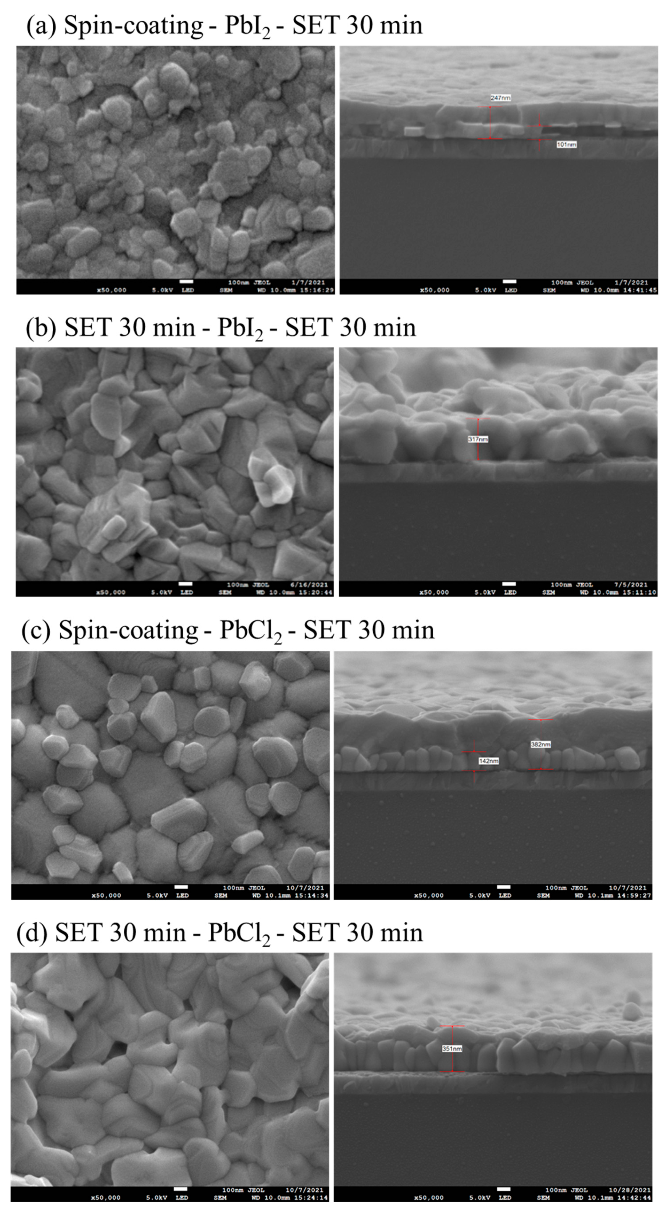
The SEM images of the top surface and cross-section morphologies of MAPbI
3 and MAPbI
xCl
3−x for spin-coating and SET 30 min is shown in
Figure 4. The SEM results clearly indicate that the grain size for the sample prepared via SET is larger than prepared via spin-coating. As the SET time increases, the uniformity, density and the smoothness of the film enhanced with the increase in the grain size and the decrease in pin-holes, which can be observed for 30 min SET time sample. Additionally, the cross-section SEM images show the presence of PbI
2 residual in the spin-coating sample. For the SET samples, the increase in the SET time has resulted in a reduction in grain accumulation and grain boundaries, with more regularity in the grain size as compared to spin-coating. Furthermore, with an increase in SET time, the MAI availability is more for the reaction with PbCl
2 and the 30 min SET time clearly shows columnar crystal with less grain boundaries for MAPbI
xCl
3−x. The ratio of Cl/(I + Cl) is an important parameter for the optimized efficiency of the perovskite. According to the EDS result, the ratio of Cl/(I + Cl) shows that if the ratio is higher than five, the excess amount of chlorine with iodide being lesser in content results in inhibiting the replacement of I
− from Cl
− for the formation of MAPbI
xCl
3−x. Whereas, for the ratio range of between 2–5, the perovskite is in a transition state with MAPbI
3 and MAPbI
xCl
3−x existing simultaneously. For a ratio lower than two, iodide is in excess, with a lesser amount of chlorine, which increases the probability of the MAPbI
xCl
3−x complete formation.
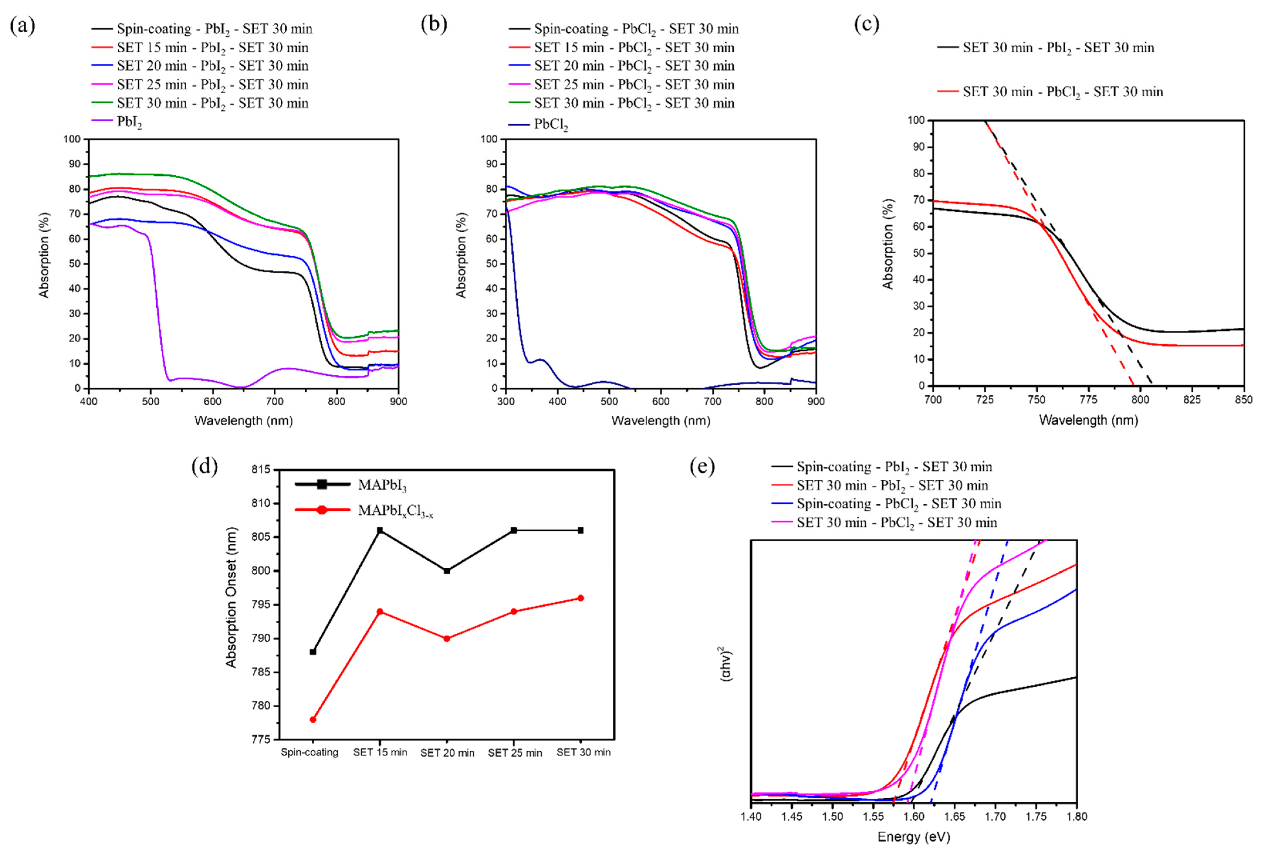
In order to investigate the optical properties of the various perovskite structure formed via the spin-coating and SET technique, we measured the UV-visible absorption spectra of the so-formed perovskite films and examined the band-gap variation from a Tauc plot for perovskite films formed at different SET times.
Figure 5a shows the absorption spectra for PbI
2 and MAPbI
3 formed with spin-coating and SET (different time period). It is clearly seen that the absorption onset for PbI
2 is around 518 nm, with a band gap of 2.39 eV. With the change in the fabrication technique from the spin-coating to the SET method, there is a remarkable increase in the absorption (%). For this reason, we initially fabricated the perovskite solar cell under this environment. For SET 30 min, there is a clear absorption edge at 780 nm indicating the formation of MAPbI
3, which can be further verified from the XRD plot for MAPbI
3 (
Figure 5a) [
18]. A similar observation was found for MAPbI
xCl
3−x, with a significant increase in the absorption range with the increase in SET time (
Figure 5b). Furthermore, a blue shift (10 nm) was observed for MAPbI
xCl
3−x as compared to MAPbI
3, indicating the Cl inclusion (
Figure 5c,d). Halide ions have the ability to tune the band gap energy of the perovskite crystal depending on the composition profile and chlorine-based perovskite displays the largest band gap, with a sequential decrease in the band gap due to the increase in the size of halide ion-based perovskite (MAPbCl
3 > MAPbBr
3 > MAPbI
3) [
19]. In our study, from the Tauc plot profile, we can clearly depict that for both the fabrication route, the chlorine-based perovskite structure has a higher band gap, as compared to iodide (
Figure 5e) [
15].
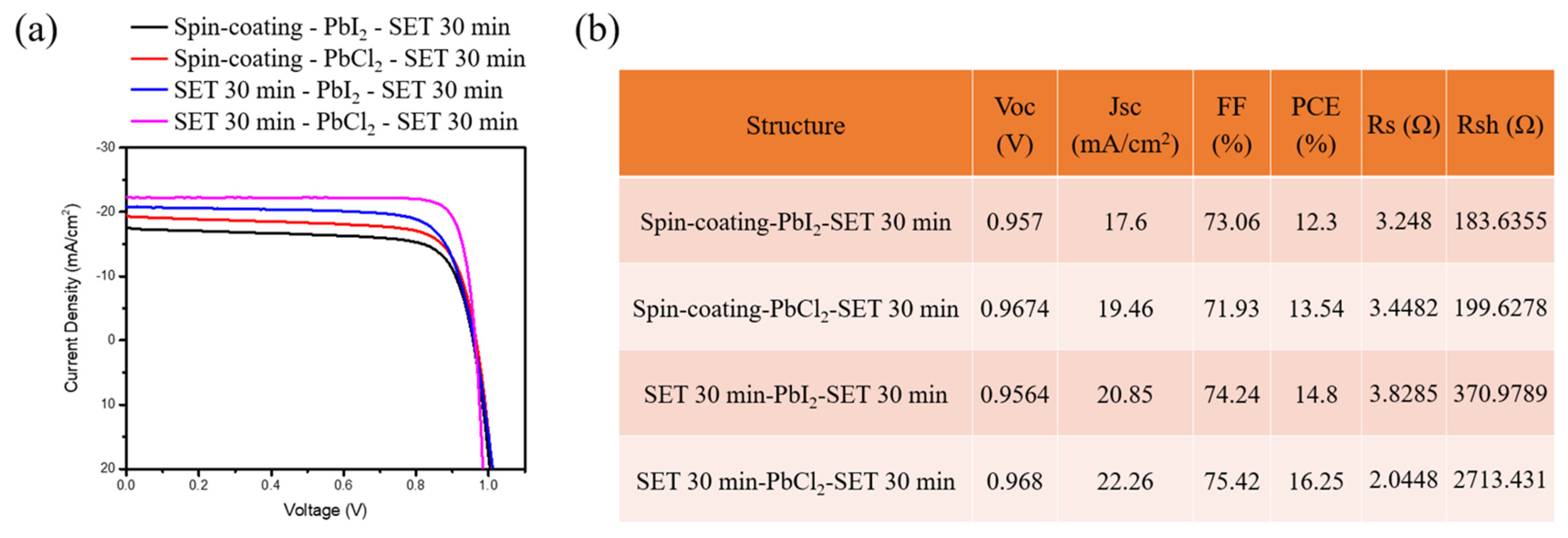
To probe the effect of the various critical parameters used in the SET based experiment on photovoltaic performance of the device, J–V curves of the two different methods (Spin-coating and SET 30 min) adopted for the MAPbI
3 and MAPbI
xCl
3−x are plotted in
Figure 6a.
Figure 6b shows the variation in PV parameters like the fill factor (FF), short-circuit current density (J
sc), and the PCE as a function of the different methods adopted. It is worth noting that the use of the SET technique resulted in higher PCE as compared to spin-coating, which is conducive to the enhancement of J
sc and FF. From the various results above, the use of DS-SET resulted in enhanced crystallinity and grain size with a lowered bandgap, and it further decreased the grain boundaries. This might be the possible pathway for electrons and holes crossing the layer interfaces. Furthermore, MAPbI
xCl
3−x has a longer diffusion length compared to MAPbI
3, which is linked with a higher PCE.
From the J–V parameter, shunt resistance (Rsh) will not have an effect on the open-circuit voltage (Voc), but can affect Jsc. Theoretically, the value of the Rsh should be infinite, close to the state of insulation, but the presence of defects in the device results in the path formation for current leakage, resulting in dropped Rsh. Furthermore, the result indicates a higher Rsh value for the DS-SET technique as compared to spin-coating, which is responsible for efficiency increment.
From the J–V characteristic curves shown in
Figure 6, the best parameter of MAPbI
3 found for the highest power conversion efficiency is SET 30 min, with V
oc = 0.9564 V, J
sc = 20.85 mA/cm
2, FF = 74.24%, PCE = 14.8%. As for the MAPbI
xCl
3−x, highest power conversion efficiency was also for SET 30 min, with V
oc = 0.968 V, J
sc = 22.26 mA/cm
2, FF = 75.42%, PCE = 16.25%.
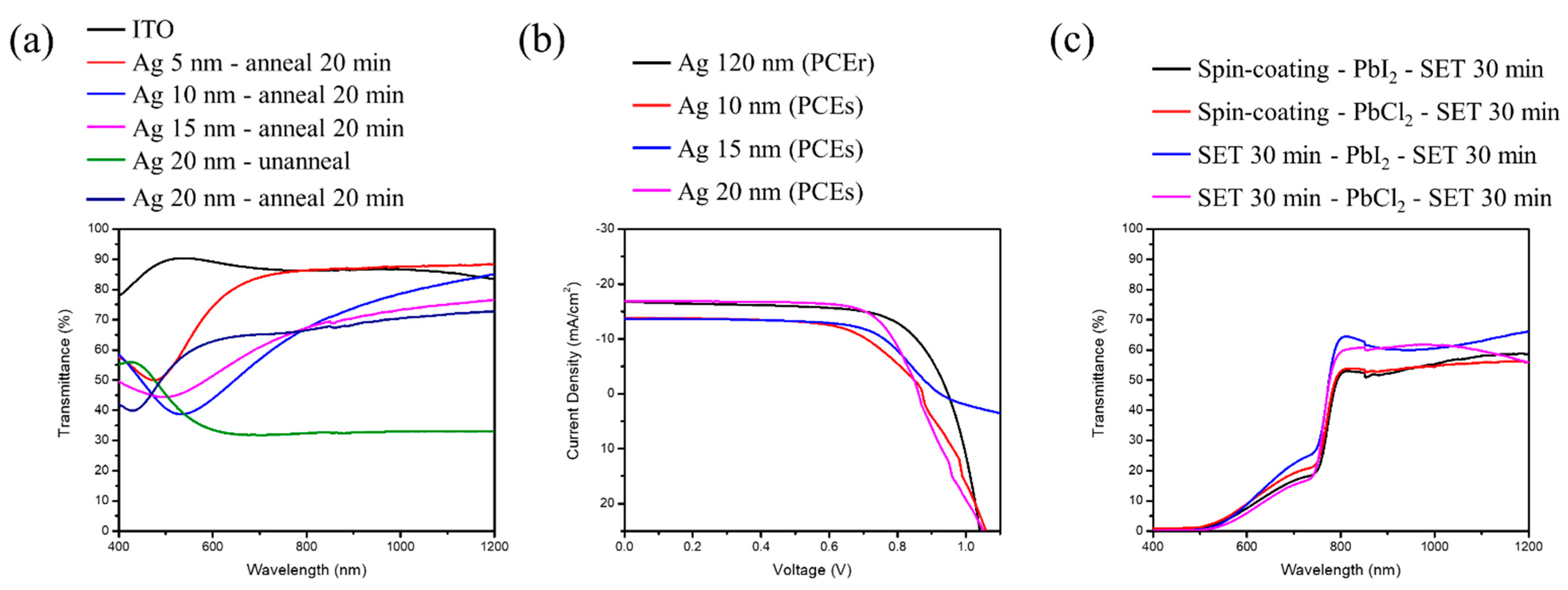
Figure 7a shows the transmission spectrum of transparent electrodes with a different thickness of Ag, annealed at 120 °C for 20 min. Note, that with an increment in the thickness, initially there was a red shift with a broadening in the position of resonance dip followed by a blue shift. From the references [
20,
21], we can realize that the position of the resonance dip is linked to localized surface plasmon resonance (LSPR) phenomenon. The reason behind the red shift is the larger diameter of the Ag nano-particles and the longer relaxation time of electrons, with an increase in the Ag thickness resulting in a lowering in the resonance frequency, leading to red shift of the resonance wavelength. Enlargement of the Ag nano-particles helps the coupling effect to become stronger, deriving larger surroundings dielectric constant. Additionally, when the distance between the Ag particles becomes less, the electromagnetic field between Ag particles will produce a coupling effect. Therefore, the resonance frequency will become higher, leading to the blue shift in the resonance wavelength.
The prime reason of higher light scattering is the presence of a rough surface, grain boundaries, and defects. However, with the annealing process of the Ag thin film, there is a remarkable reduction in surface defects with the presence of a large dense surface. As a result, reflectivity, as well as light scattering, decreases with a relative increase in transmittance.
As the resistance for lower thickness of the Ag film is too large to conduct electricity, we tried to increase the thickness of the film.
Figure 7b shows the J–V characteristics of perovskite solar cells with different silver thickness as transparent electrodes. It can be further seen from
Table 4 that the resistance value measured through the multi-meter shows that it is smallest for 20 nm, and the efficiency is maintained up to 99.07%, with a near-infrared light range transmittance average of 70.11%, which is transparent theoretically.
Figure 7c shows the transmission spectrum of perovskite solar cells with transparent electrodes of thickness 20 nm for each sandwich structure. The perovskite mainly absorbs the visible light range, and about 40–45% of the transmittance is left for the silicon solar cells underneath for absorption.
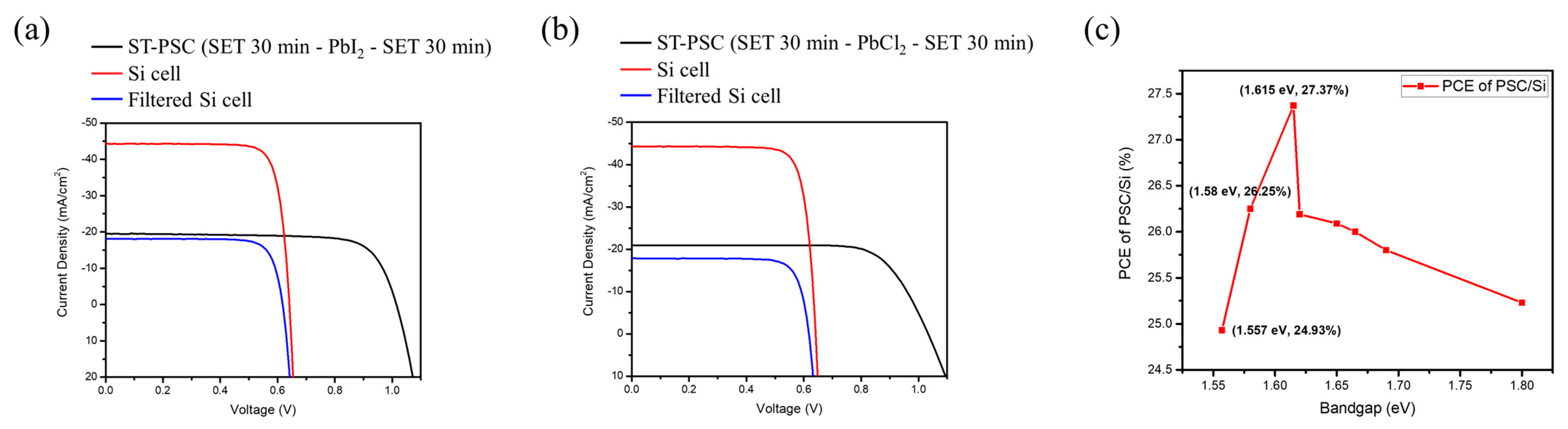
Finally, the formed perovskite solar cell is merged with the silicon solar cell via a 4T configuration for the formation of a tandem solar cell, and the result is shown in
Figure 8a,b. A PCE (%) of 23.07% is achieved for MAPbI
3 using the SET technique.
Table 5 shows the upper semitransparent PSC had an efficiency of 14.6% with photovoltaic parameter being V
oc = 1.02 V, J
sc = 19.6 mA/cm
2, and FF = 73.57%, while the lower silicon solar cell had an efficiency of 8.47% with V
oc = 0.62 V, J
sc = 18.1 mA/cm
2, and FF = 75.45%.
As for MAPbIxCl3−x using SET up to 24.43% is achieved. The upper semitransparent PSC had an efficiency of 16.1%, Voc = 1.037 V, Jsc = 20.9 mA/cm2, and FF = 74.25%. The lower silicon solar cell had an efficiency of 8.33%, Voc = 0.618 V, Jsc = 17.8 mA/cm2, and FF = 75.54%.
Figure 8c shows the SETFOS simulation results for the PSC/Si tandem solar cell at some certain perovskite bandgaps. From the results, we remark that the efficiency has an increase trend between 1.55–1.62 eV. Compared with our experimental data, it shows the same PCE (%) trend of PSC/Si with an increment in bandgap from MAPbI
3 to MAPbI
xCl
3−x, which is located in the range. The above result depicts that using a suitable bandgap of the perovskite matched with silicon to form a tandem solar cell can effectively absorb the solar spectrum to attain the highest usage.
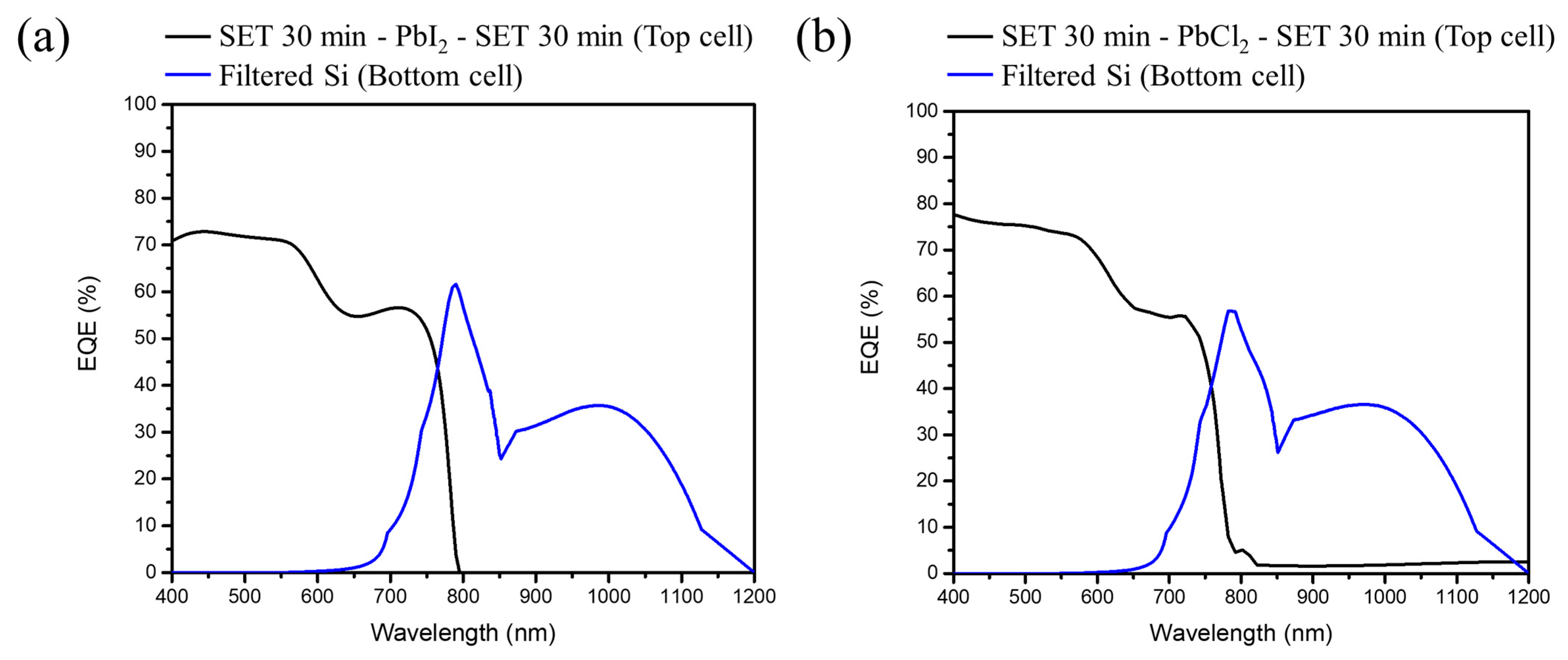
Figure 9 presents the EQE spectra of the perovskite/Si tandem solar cell with a different perovskite sandwich structure as the top cell.
Figure 9a,b corresponds to the
Figure 8a,b, respectively. It displays the spectra in the spectral range of 400–800 nm with a highest EQE value up to ~70% for the iodide and ~75% for chloride based perovskite structure at λ = 575 nm, respectively. Besides, the top cell with a chlorine based perovskite shows a higher EQE rate and ~5 nm blue shift onset as compared to the iodide based perovskite, which can be further linked with the results of lattice shrinkage obtained from XRD, blue shift in the absorption spectra, and the increment of current density from MAPbI
3 to MAPbI
xCl
3−x.


