
Selective Mid-IR Metamaterial-Based Gas Sensor System: Proof of Concept and Performances Tests


Abstract
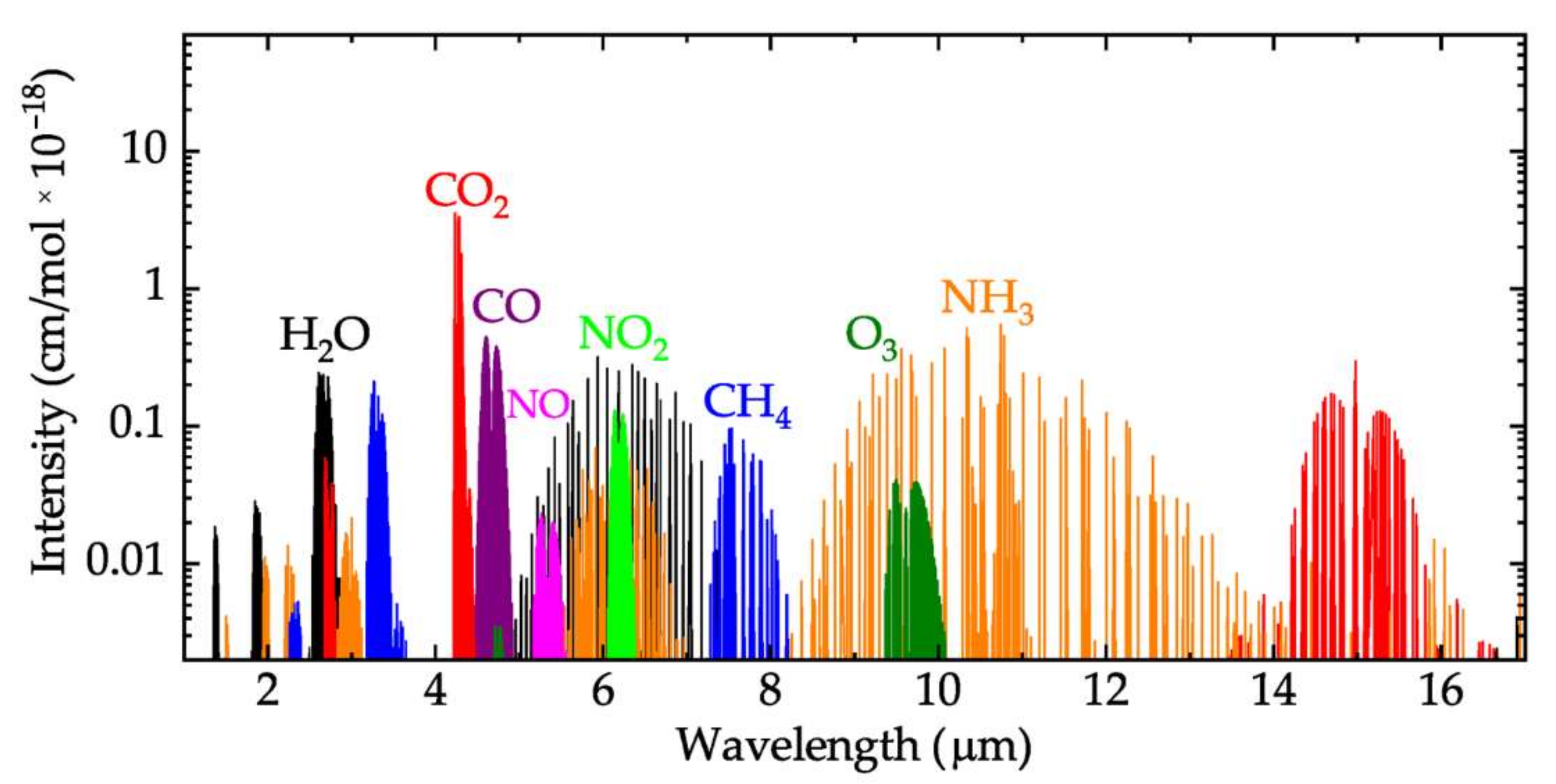
:1. Introduction
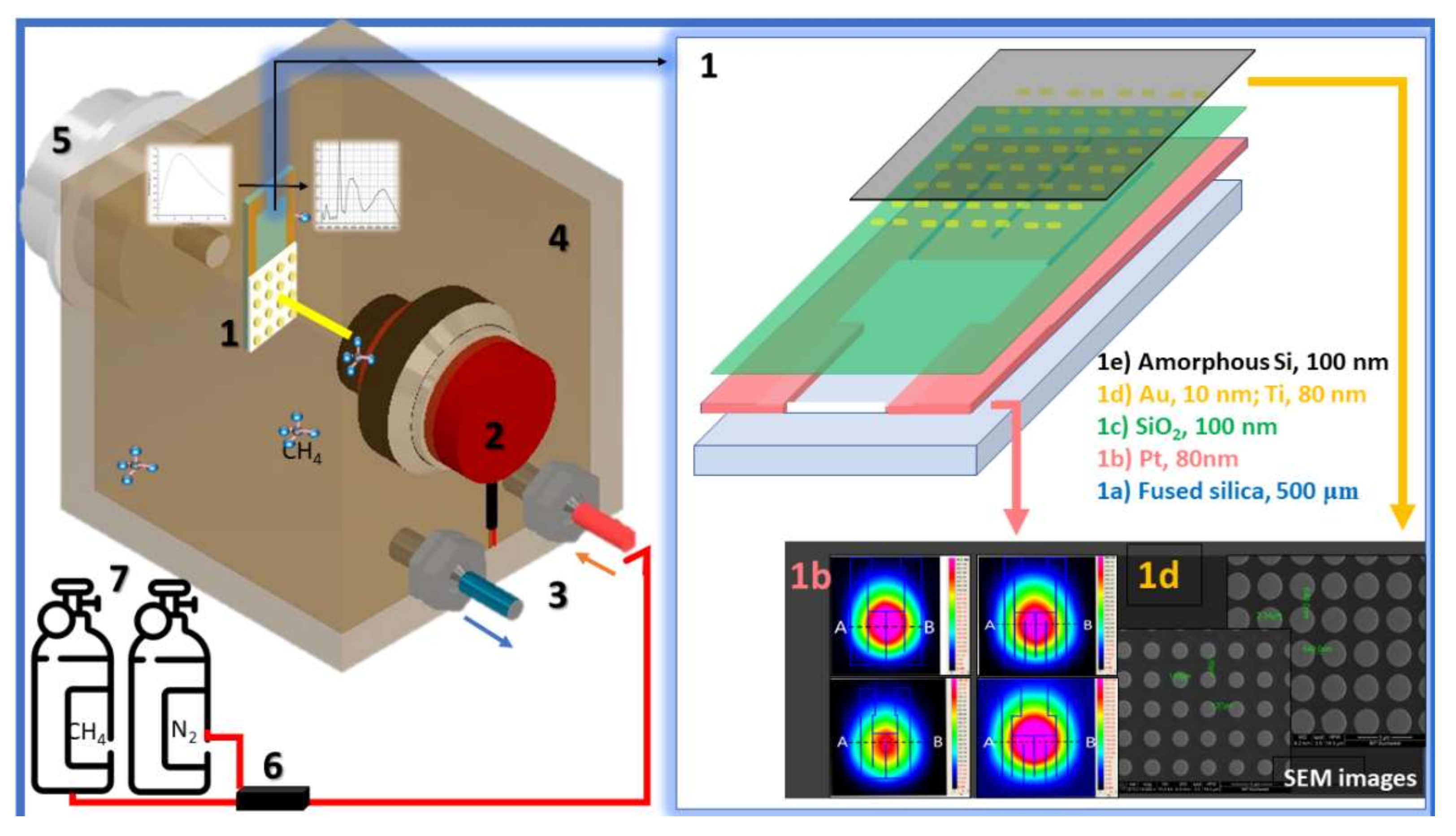
2. Sensor Structure and Technology Process
3. Characterization Methods; Results and Discussion
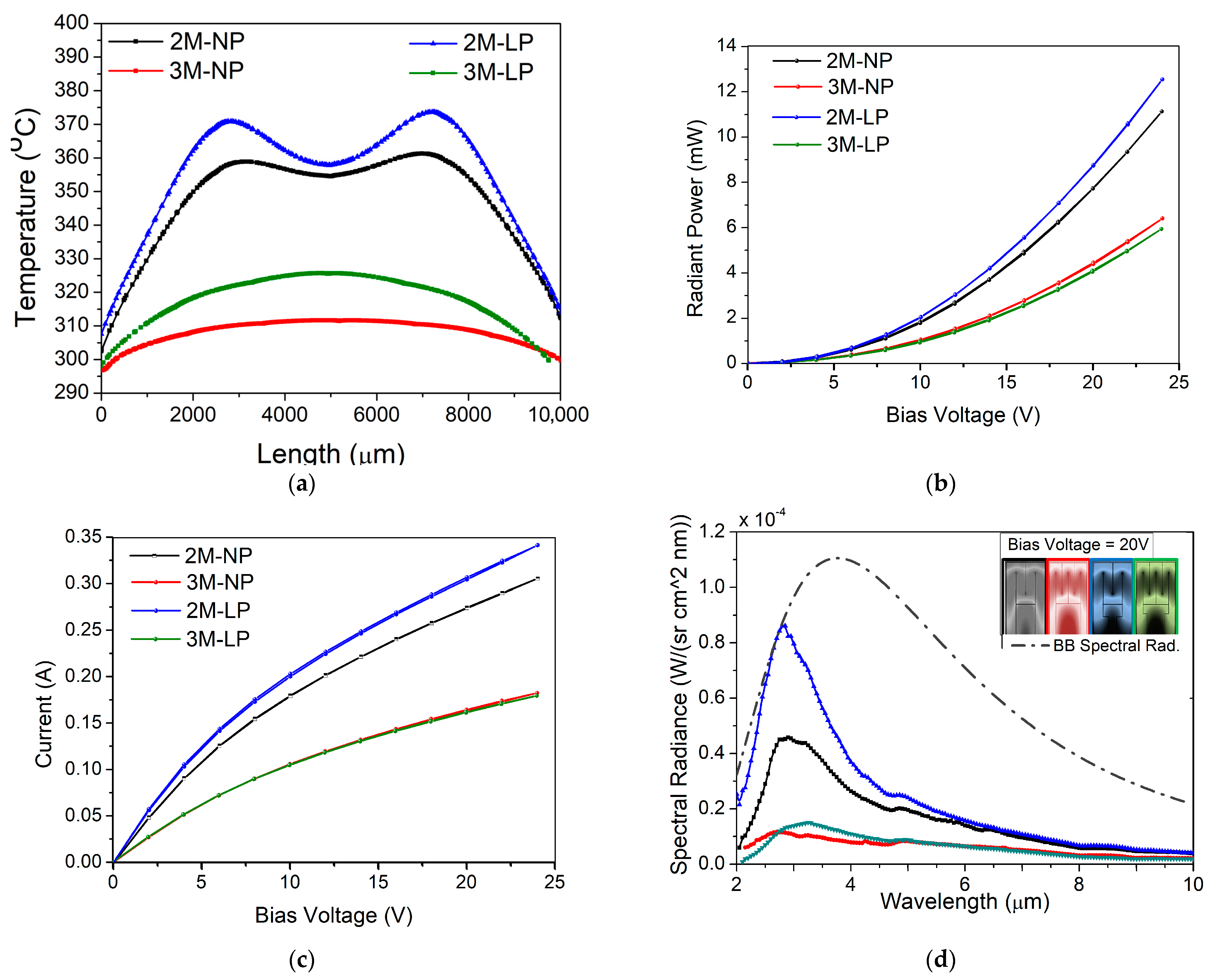
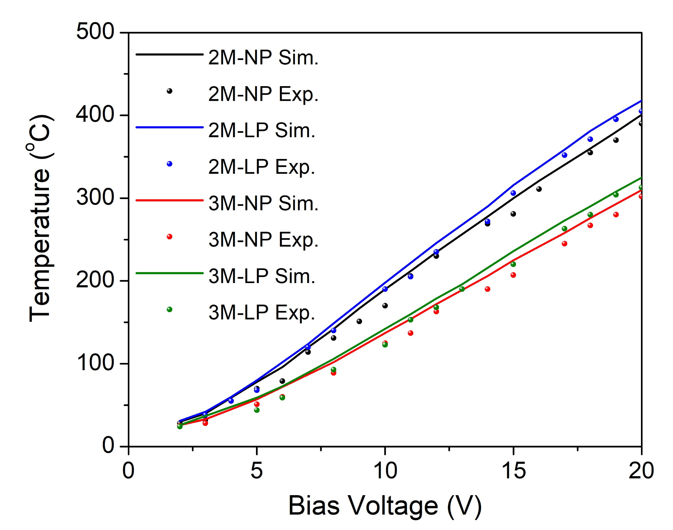
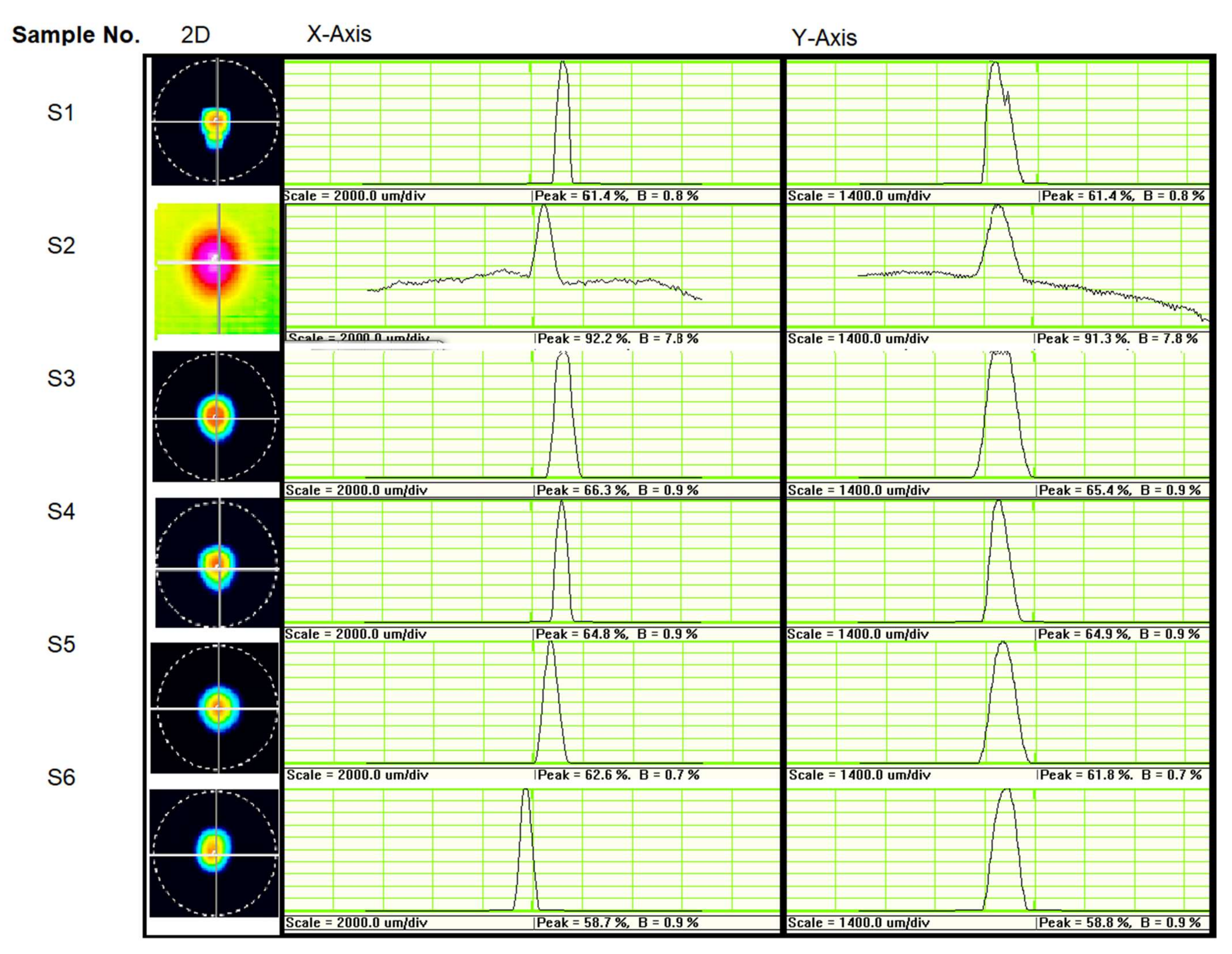
3.1. Microheater Capabilities
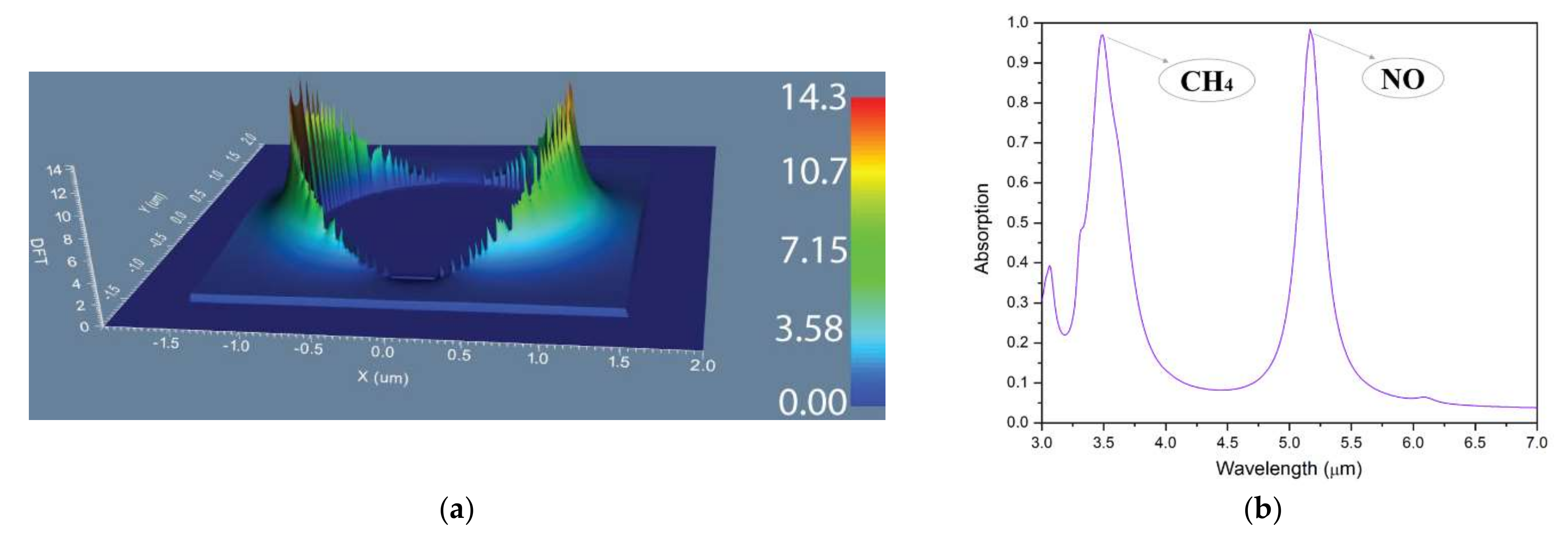
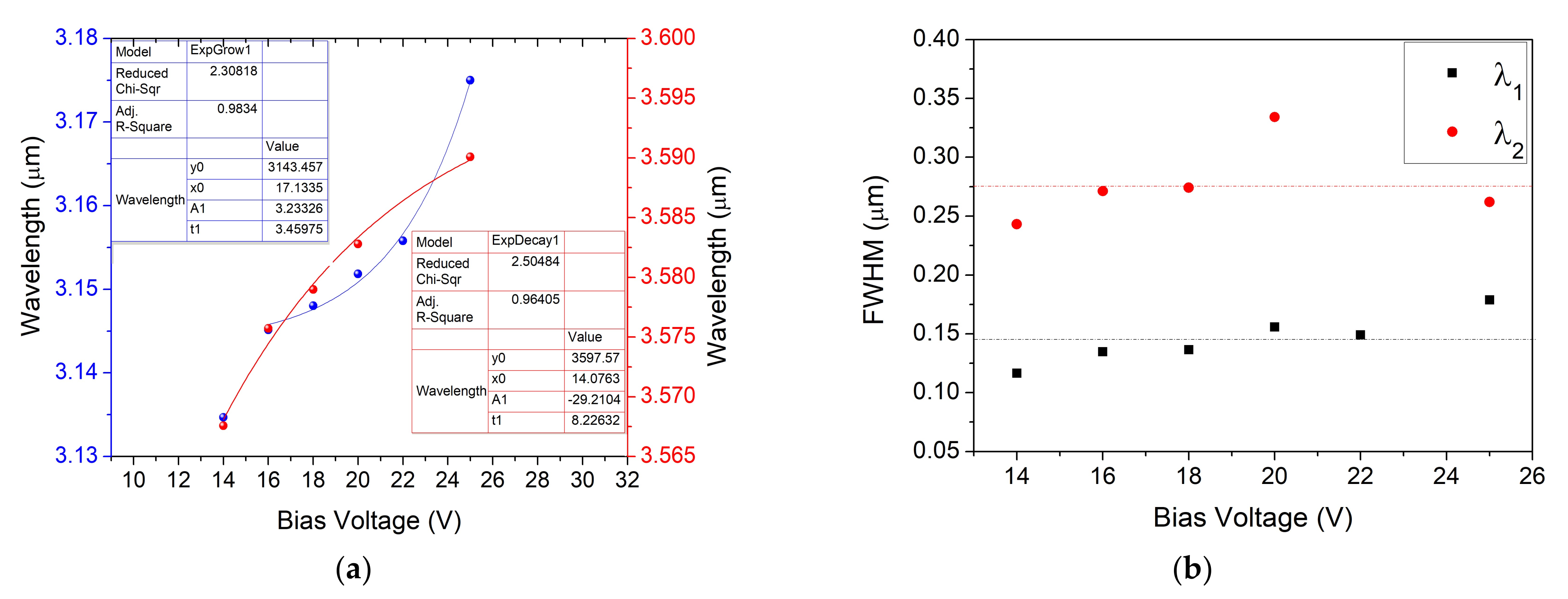
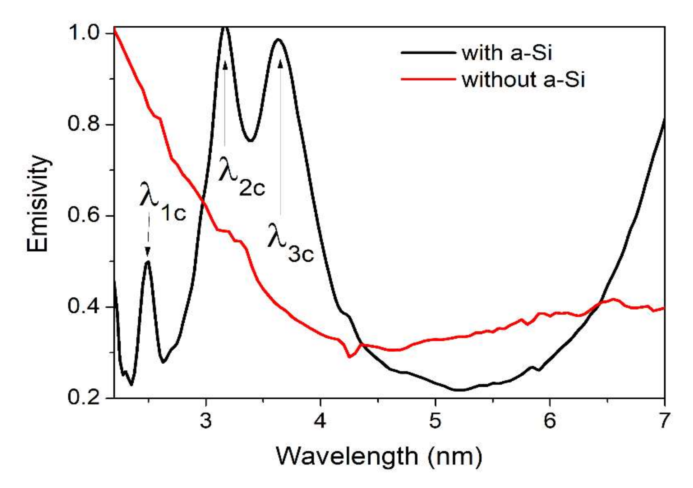
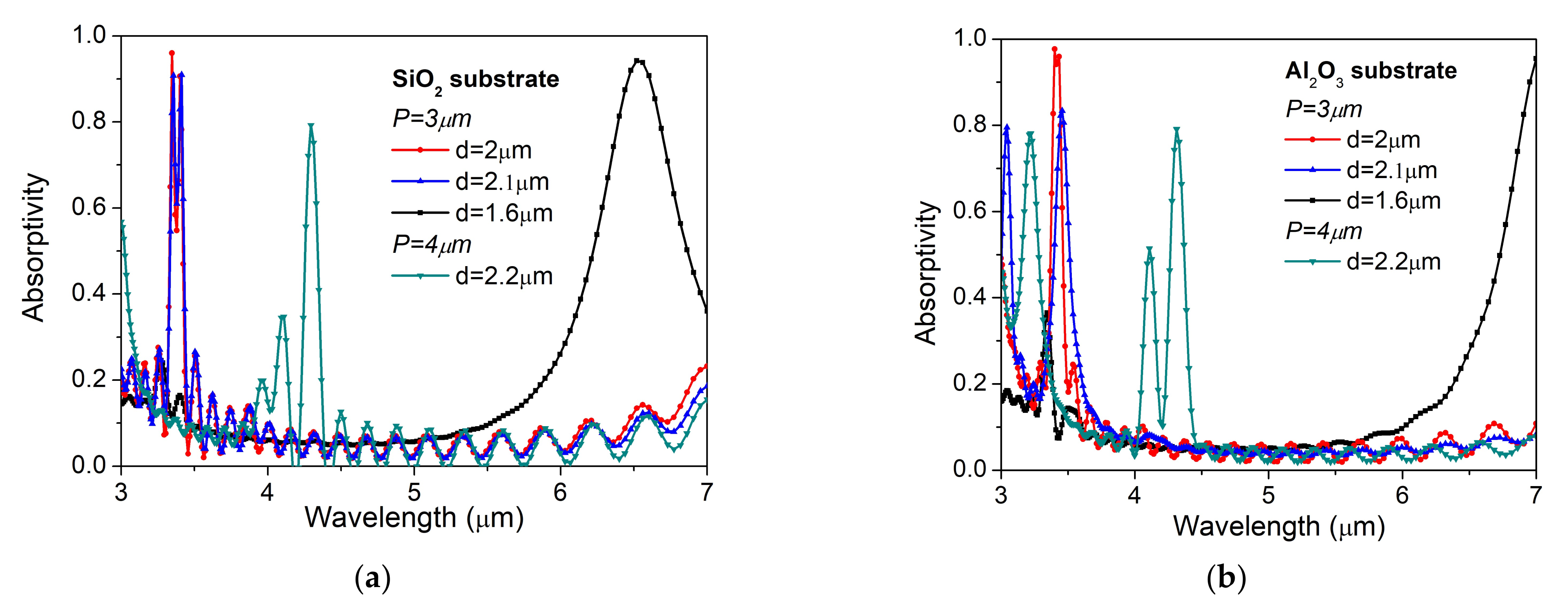
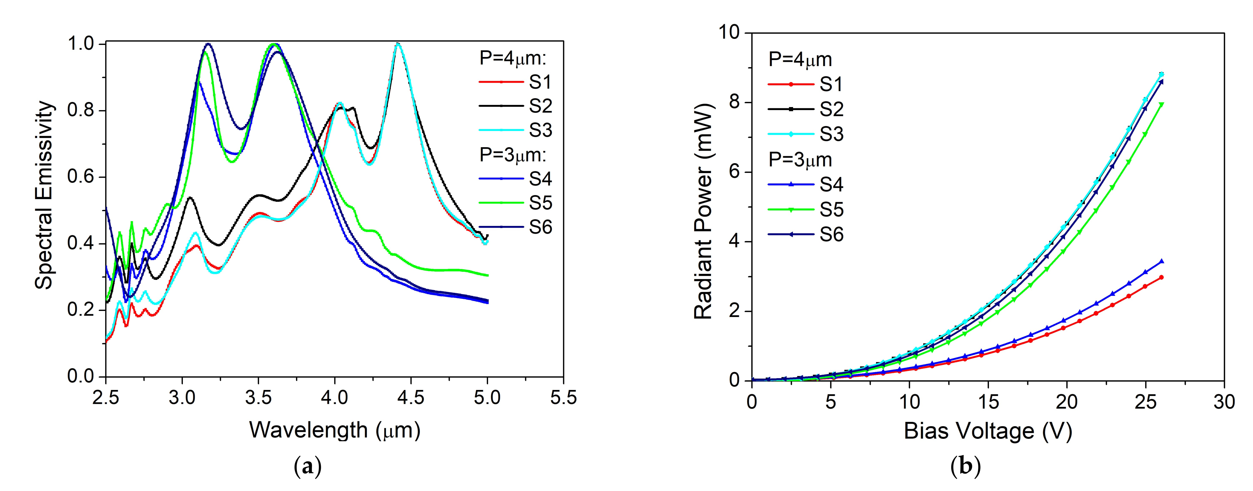
3.2. Metamaterial IR Selective Emitter Capabilities
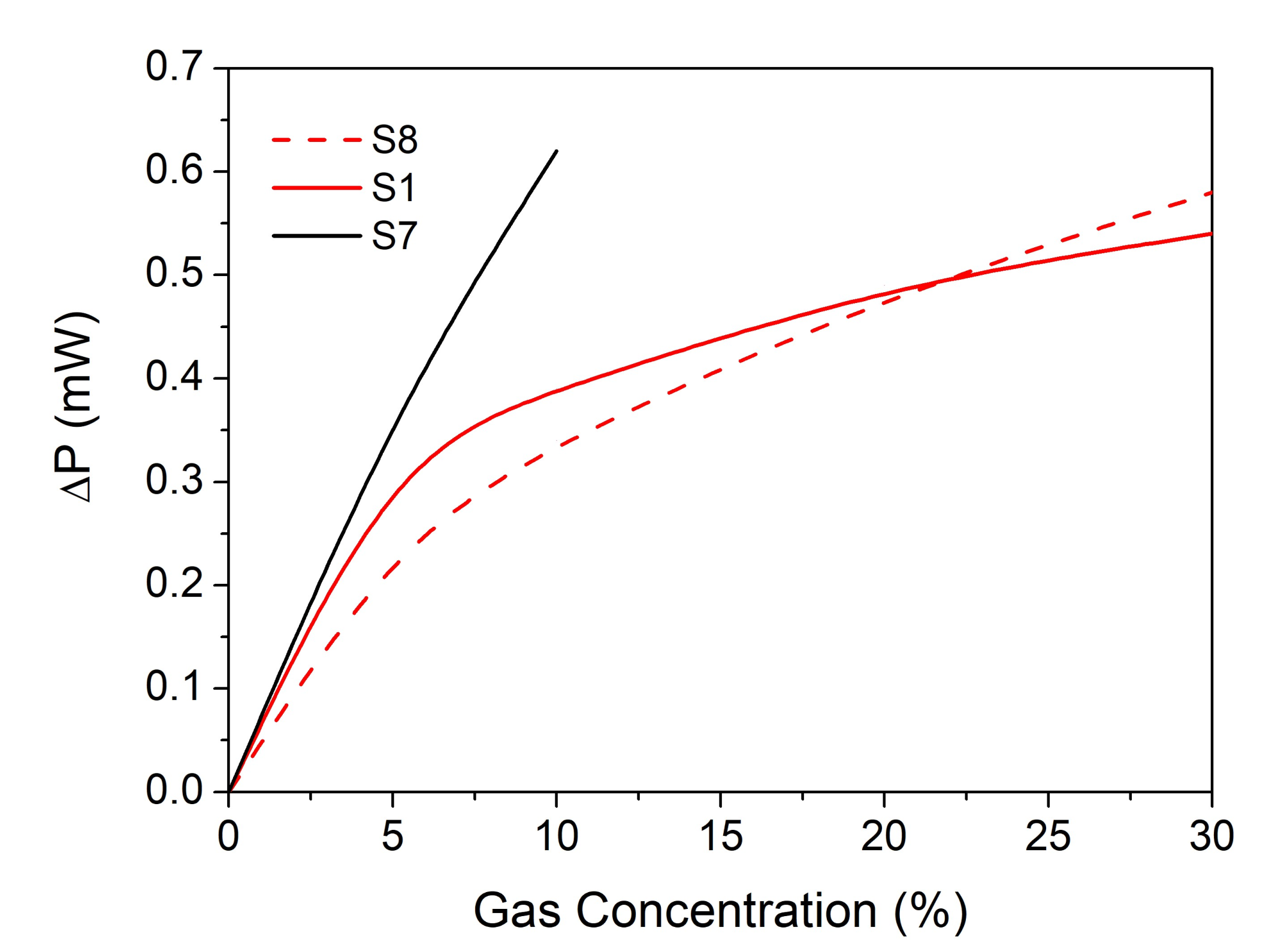
3.3. Sensor Functionality Test
4. Conclusions
Author Contributions
Funding
Institutional Review Board Statement
Informed Consent Statement
Data Availability Statement
Conflicts of Interest
References
- Kumar, P.; Morawska, L.; Martani, C.; Biskos, G.; Neophytou, M.K.-A.; Di Sabatino, S.; Bell, M.; Norford, L.; Britter, R. The rise of low-cost sensing for managing air pollution in cities. Environ. Int. 2015, 75, 199–205. [Google Scholar] [CrossRef] [PubMed] [Green Version]
- Lochbaum, A.; Dorodnyy, A.; Koch, U.; Koepfli, S.M.; Volk, S.; Fedoryshyn, Y.; Wood, V.; Leuthold, J. Compact mid-infrared gas sensing enabled by an all-metamaterial design. Nano Lett. 2020, 20, 4169–4176. [Google Scholar] [CrossRef]
- Dong, L.; Tittel, F.K.; Li, C.; Sanchez, N.P.; Wu, H.; Zheng, C.; Yu, Y.; Sampaolo, A.; Griffin, R.J. Compact TDLAS based sensor design using interband cascade lasers for mid-IR trace gas sensing. Opt. Express 2016, 24, A528–A535. [Google Scholar] [CrossRef] [PubMed]
- Timothy, D.; Michael, P.; Dave, C.; Kristen, C.; Ron, A.; Alex, W.; Michael, H.; Eric, B.T. Quantum cascade lasers for defense and security. Technologies for Optical Countermeasures X; and High-Power Lasers 2013: Technology and Systems. Proc. SPIE 2013, 8898, 889802. [Google Scholar] [CrossRef]
- Fuchs, P.; Seufert, J.; Koeth, J.; Semmel, J.; Höfling, S.; Worschech, L.; Forchel, A. Widely tunable quantum cascade lasers with coupled cavities for gas detection. Appl. Phys. Lett. 2010, 97, 181111. [Google Scholar] [CrossRef]
- Wang, W.; Wang, Y.; Song, W.; Li, X. Multiband infrared inversion for low-concentration methane monitoring in a confined dust-polluted atmosphere. Appl. Opt. 2017, 56, 2548. [Google Scholar] [CrossRef] [PubMed]
- Wang, J.; Zheng, L.; Niu, X.; Zheng, C.; Wang, Y.; Tittel, F.K. Mid-infrared absorption-spectroscopy-based carbon dioxide sensor network in greenhouse agriculture: Development and deployment. Appl. Opt. 2016, 55, 7029–7036. [Google Scholar] [CrossRef] [PubMed]
- Jones, A.; Lam, P. End-expiratory carbon monoxide levels in healthy subjects living in a densely populated urban environment. Sci. Total Environ. 2006, 354, 150–156. [Google Scholar] [CrossRef] [PubMed]
- Ostro, B.; Spadaro, J.V.; Gumy, S.; Mudu, P.; Awe, Y.; Forastiere, F.; Peters, A. Assessing the recent estimates of the global burden of disease for ambient air pollution: Methodological changes and implications for low- and middle-income countries. Environ. Res. 2018, 166, 713–725. [Google Scholar] [CrossRef]
- Open-Ended CPR. Healthy Environment, Healthy People. 2016, pp. 3–4. Available online: http://www.pnuma.org/forodeministros/20-colombia/documentos/HEHP_draft_report_CPR.pdf (accessed on 14 February 2022).
- WHO. Air Quality Guidelines: Global Update 2005: Particulate Matter, Ozone, Nitrogen Dioxide, and Sulfur Dioxide. World Health Organization, Copenhagen. 2006. Available online: https://apps.who.int/iris/handle/10665/69477 (accessed on 14 February 2022).
- Manisalidis, I.; Stavropoulou, E.; Stavropoulos, A.; Bezirtzoglou, E. Environmental and health impacts of air pollution: A review. Front. Public Health 2020, 8, 14. [Google Scholar] [CrossRef] [Green Version]
- Mannucci, P.M.; Franchini, M. Health effects of ambient air pollution in developing countries. Int. J. Environ. Res. Public Health 2017, 14, 1048. [Google Scholar] [CrossRef] [PubMed]
- Gordon, I.E.; Rothman, L.S.; Hill, C.; Kochanov, R.V.; Tan, Y.; Bernath, P.F.; Birk, M.; Boudon, V.; Campargue, A.; Chance, K.V.; et al. The HITRAN2016 molecular spectroscopic database. J. Quant. Spectrosc. Radiat. Transf. 2017, 203, 3–69. [Google Scholar] [CrossRef]
- Pinto, D.; Moser, H.; Waclawek, J.P.; Russo, S.D.; Patimisco, P.; Spagnolo, V.; Lendl, B. Parts-per-billion detection of carbon monoxide: A comparison between quartz-enhanced photoacoustic and photothermal spectroscopy. Photoacoustics 2021, 22, 100244. [Google Scholar] [CrossRef]
- Ye, W.; Li, C.; Zheng, C.; Sanchez, N.P.; Głuszek, A.; Hudzikowski, A.J.; Dong, L.; Griffin, R.J.; Tittel, F.K. Mid-infrared dual-gas sensor for simultaneous detection of methane and ethane using a single continuous-wave interband cascade laser. Opt. Express 2016, 24, 16973–16985. [Google Scholar] [CrossRef] [PubMed]
- Bidaux, Y.; Bismuto, A.; Patimisco, P.; Sampaolo, A.; Gresch, T.; Strubi, G.; Blaser, S.; Tittel, F.K.; Spagnolo, V.; Muller, A.; et al. Mid infrared quantum cascade laser operating in pure amplitude modulation for background-free trace gas spectroscopy. Opt. Express 2016, 24, 26464–26471. [Google Scholar] [CrossRef]
- Willer, U.; Saraji, M.; Khorsandi, A.; Geiser, P.; Schade, W. Near- and mid-infrared laser monitoring of industrial processes, environment and security applications. Opt. Lasers Eng. 2006, 44, 699–710. [Google Scholar] [CrossRef]
- Yang, J.; Zhou, J.; Lin, P.T. Real-time isotopic methane detection using mid-infrared spectroscopy. Appl. Opt. 2020, 59, 10801–10807. [Google Scholar] [CrossRef]
- Shahmarvandi, E.K.; Ghaderi, M.; Ayerden, P.; de Graaf, G.; Wolffenbuttel, R. Implementation of CMOS-compatible metamaterial absorber for gas sensing application. Procedia Eng. 2016, 168, 1241–1244. [Google Scholar] [CrossRef]
- Hasan, D.; Lee, C. Hybrid metamaterial absorber platform for sensing of CO2 gas at Mid-Ir. Adv. Sci. 2018, 5, 1700581. [Google Scholar] [CrossRef]
- Xu, R.; Lin, Y.-S. Tunable infrared metamaterial emitter for gas sensing application. Nanomaterials 2020, 10, 1442. [Google Scholar] [CrossRef]
- Cao, J.; Liu, X.; Chang, Q.; Yang, Z.; Zhou, H.; Fan, T. Spectrally tunable nanocomposite metamaterials as near-perfect emitters for mid-infrared thermal radiation management. Phys. Chem. Chem. Phys. 2020, 22, 28012–28020. [Google Scholar] [CrossRef] [PubMed]
- Livingood, A.; Nolen, J.R.; Folland, T.G.; Potechin, L.; Lu, G.; Criswell, S.; Maria, J.P.; Shelton, C.T.; Sachet, E.; Caldwell, J.D. Filter less nondispersive infrared sensing using narrowband infrared emitting metamaterials. ACS Photonics 2021, 8, 472–480. [Google Scholar] [CrossRef]
- Zheng, D.; Lin, Y.-S. Tunable dual-split-disk resonator with electromagnetically induced transparency characteristic. Adv. Mater. Technol. 2020, 5, 2000584. [Google Scholar] [CrossRef]
- Han, Y.; Lin, J.; Lin, Y.-S. Tunable metamaterial-based silicon waveguide. Opt. Lett. 2020, 45, 6619–6622. [Google Scholar] [CrossRef]
- Wei, J.; Ren, Z.; Lee, C. Metamaterial technologies for miniaturized infrared spectroscopy: Light sources, sensors, filters, detectors, and integration. J. Appl. Phys. 2020, 128, 240901. [Google Scholar] [CrossRef]
- Ran, L.; Tao, Y.; Guo, K.; Shen, F.; Zhou, H.; Sun, Y.; Zhang, R.; Zhou, Q.; Yang, J.; Yin, Z.; et al. Bias-scanning based tunable LSPR sensor. Phys. Chem. Chem. Phys. 2018, 20, 2146–2150. [Google Scholar] [CrossRef]
- Selvakumar, V.S.; Sujatha, L.; Sundar, R. A Novel MEMS microheater based alcohol gas sensor using nanoparticles. J. Semicond. Technol. Sci. 2018, 18, 445–453. [Google Scholar] [CrossRef]
- Tomescu, R.; Kusko, C.; Cristea, D.; Calinoiu, R.; Parvulescu, C. Nano-pillars metasurface modelled for perfect absorption at specific wavelengths in infrared spectral regime. Solid State Electron. Lett. 2020, 2, 146–150. [Google Scholar] [CrossRef]
- Davids, P.S.; Kirsch, J.; Starbuck, A.; Jarecki, R.; Shank, J.; Peters, D. Electrical power generation from moderate-temperature radiative thermal sources. Science 2020, 367, 1341–1345. [Google Scholar] [CrossRef]
- Wu, S.; Lin, Q.; Yuen, Y.; Tai, Y.-C. MEMS flow sensors for nano-fluidic applications. Sens. Actuators A Phys. 2001, 89, 152–158. [Google Scholar] [CrossRef] [Green Version]
- Paun, C.; Tomescu, R.; Parvulescu, C.; Ionescu, O.; Gavrila, D.E.; Cristea, D. Microheater optimized for the integration with metasurface-based IR sources for gas sensing application. Sci. Technol. 2021, 24, 201–212. [Google Scholar]
- Ophir. High Sensitivity Thermal Sensors. Available online: https://www.ophiropt.com/laser--measurement/sites/default/files/3A-P-THz_3A-FS_3A-P-FS-12.pdf (accessed on 17 February 2022).


 | No. | Disk Diameterd (µm) | Disk Period P (µm) | Absorption Peak A (µm) | Type of Gas |
| 1 | 1.6 | 3 | 3.6 | CH4/formaldehyde | |
| 2 | 2 | 3 | 3.4/5.1 | CH4/NO | |
| 3 | 2.1 | 3 | 6.3/3.3 | NO2/CH4 | |
| 4 | 1.5 | 4.5 | 5.11 | NO | |
| 5 | 1.3 | 4 | 4.46/4.95 | CO | |
| 6 | 1.4 | 4 | 5 | NO/CO | |
| 7 | 1.7 | 4 | 4.15/5.6 | CO2/NO | |
| 8 | 2.2 | 4 | 4.15 | CO2 |
| Sample | Meanders | Pads | d (μm) | P (μm) | Spectral Range (μm) | Main Peak (μm) | Second Peak (μm) | Third Peak (μm) | Corresponding to Gas Molecule Abs. Peak |
|---|---|---|---|---|---|---|---|---|---|
| S1 | 3 | Narrow | 2.2 | 4 | 3.9...4.16 4.25...4.55 | 4.41 | 4.03 | 3.09 | NO2, CO2 |
| S2 | 2 | Narrow | 2.2 | 4 | 3.9...4.2 4.37...4.43 | 4.41 | 4.04 | 3.05 | NO2, CO2 |
| S3 | 2 | Large | 2.2 | 4 | 3.91...4.17 4.25...4.5 | 4.41 | 4.04 | 3.09 | NO2, CO2 |
| S4 | 3 | Large | 2 | 3 | 3.1...3.3 | 3.17 | 3.62 | - | CH4 |
| S5 | 2 | Large | 2.1 | 3 | 3.08...3.23 | 3.61 | 3.11 | - | CH4 |
| S6 | 2 | Large | 1.6 | 3 | 3.05...3.2 | 3.6 | 3.15 | - | CH4 |
| S7 | 2 | Narrow | 1.2 | 3 | 3.1...3.2 3.9...4.35 | 3.15 | 4.05 | 4.3 | CH4, CO2 |
| S8 | 3 | Narrow | 1.4 | 4 | 4.2…4.6 | 4.4 | 6 | - | CO2 |
| S9 | 2 | Large | 1.3 | 4 | 4.3…4.8 | 4.5 | 6.1 | - | CO |
Publisher’s Note: MDPI stays neutral with regard to jurisdictional claims in published maps and institutional affiliations. |
© 2022 by the authors. Licensee MDPI, Basel, Switzerland. This article is an open access article distributed under the terms and conditions of the Creative Commons Attribution (CC BY) license (https://creativecommons.org/licenses/by/4.0/).
Share and Cite
Mihai, L.; Mihalcea, R.; Tomescu, R.; Paun, C.; Cristea, D. Selective Mid-IR Metamaterial-Based Gas Sensor System: Proof of Concept and Performances Tests. Nanomaterials 2022, 12, 1009. https://doi.org/10.3390/nano12061009
Mihai L, Mihalcea R, Tomescu R, Paun C, Cristea D. Selective Mid-IR Metamaterial-Based Gas Sensor System: Proof of Concept and Performances Tests. Nanomaterials. 2022; 12(6):1009. https://doi.org/10.3390/nano12061009
Chicago/Turabian StyleMihai, Laura, Razvan Mihalcea, Roxana Tomescu, Costel Paun, and Dana Cristea. 2022. "Selective Mid-IR Metamaterial-Based Gas Sensor System: Proof of Concept and Performances Tests" Nanomaterials 12, no. 6: 1009. https://doi.org/10.3390/nano12061009
APA StyleMihai, L., Mihalcea, R., Tomescu, R., Paun, C., & Cristea, D. (2022). Selective Mid-IR Metamaterial-Based Gas Sensor System: Proof of Concept and Performances Tests. Nanomaterials, 12(6), 1009. https://doi.org/10.3390/nano12061009