Article

Design and Optimize the Performance of Self-Powered Photodetector Based on PbS/TiS3 Heterostructure by SCAPS-1D

Key Laboratory of Instrumentation Science and Dynamic Measurement, Ministry of Education, School of Instrument and Electronics, North University of China, Taiyuan 030051, China
*
Author to whom correspondence should be addressed.
Nanomaterials 2022, 12(3), 325; https://doi.org/10.3390/nano12030325
Submission received: 23 December 2021 / Revised: 10 January 2022 / Accepted: 17 January 2022 / Published: 20 January 2022

Abstract

:
Titanium trisulphide (TiS3) has been widely used in the field of optoelectronics owing to its superb optical and electronic characteristics. In this work, a self-powered photodetector using bulk PbS/TiS3 p-n heterojunction is numerically investigated and analyzed by a Solar Cell Capacitance Simulator in one-Dimension (SCAPS-1D) software. The energy bands, electron-holes generation or recombination rate, current density-voltage (J-V), and spectral response properties have been investigated by SCAPS-1D. To improve the performance of photodetectors, the influence of thickness, shallow acceptor or donor density, and defect density are investigated. By optimization, the optimal thickness of the TiS3 layer and PbS layer are determined to be 2.5 μm and 700 nm, respectively. The density of the superior shallow acceptor (donor) is 1015 (1022) cm−3. High quality TiS3 film is required with the defect density of about 1014 cm−3. For the PbS layer, the maximum defect density is 1017 cm−3. As a result, the photodetector based on the heterojunction with optimal parameters exhibits a good photoresponse from 300 nm to 1300 nm. Under the air mass 1.5 global tilt (AM 1.5G) illuminations, the optimal short-circuit current reaches 35.57 mA/cm2 and the open circuit voltage is about 870 mV. The responsivity (R) and a detectivity (D*) of the simulated photodetector are 0.36 A W1 and 3.9 × 10¹³ Jones, respectively. The simulation result provides a promising research direction to further broaden the TiS3-based optoelectronic device.

1. Introduction

Photodetectors that directly convert light into electrical signals have been developed for numerous applications, including medical diagnosis, aviation, target recognition, missile warning, and other fields [1,2,3,4,5,6,7]. Recently, self-powered photodetectors which can realize light detection without an external power supply have aroused a great deal of interest. The self-powered devices can work independently because of the photoelectric effect based on p–n or Schottky junction under illumination from light sources [8]. The built-in electric field existing in effective heterojunction between different materials will function as a driving force for high efficiency photogenerated carriers’ separation and produce continuous photocurrent. Photodetectors with self-powered behaviors based on p–n junction exhibit outstanding photoelectric performance, such as high response speed, large linear region, and low noise, and have achieved significant progresses [9].
Titanium trisulphide (TiS3) with a monoclinic structure is an n-type semiconducting material which has a direct optical bandgap of 1.0 eV [10,11]. Theoretically, TiS3 will be a potential candidate substitution to silicon, micro or nanostructured, due to its exceptional carrier mobility (as high as ~104 cm2 V−1 s−1), high anisotropy, high optical absorption coefficient, and high chemical stability in the open-air [12,13]. Typically, the TiS3 nanoribbon material has been successfully obtained in laboratory by sulfuration of Ti film. The unique optoelectronics properties of TiS3 nanostructure make it wildly useful in the fields of cathodes in batteries [14,15], hydrogen storage [16,17], thermoelectric energy conversion devices [18,19,20], and optoelectronics applications [21,22,23,24]. Niu et al. have developed a mixed-dimensionality TiS3/Si n–p heterostructure broadband photodetector via staking an n-type TiS3 nanoribbon onto p-type silicon substrate. The photoresponse of the device strongly depends on the polarization direction of the illumination. The high responsivity and on/off ratio of the TiS3/Si device were ascribed to the improvement in charge separation coming from the coupling effect of TiS3 nanoribbon and Si substrate [25]. Frisenda et al. have fabricated TiS3-based nanoribbon photodetectors by the dielectrophoresis method between two gold electrodes. The photodetector can work efficiently in the visible region and possesses a responsivity of 3.8 mA/W [26]. Huang et al. synthesized TiS3 nanoribbon array film on Ti-coated glass-carbon substrate by using a chemical vapor transport method. The vertically grown TiS3 film with moderate S22− vacancies exhibits a long electron diffusion length for collecting electrons efficiently and an outstandingly high photocurrent density of 15.35 mA/cm2 was achieved at 1.4 V versus using reversible hydrogen electrode [27]. The TiS3 film has been proven as an excellent photoanode material. However, there are few reports concerning the self-powered photodetector using the TiS3 film.
In this work, a self-powered PbS/TiS3 p–n heterojunction film photodetector is numerically investigated and analyzed by one-Dimension software SCAPS-1D. By numerically modeling, the impact of thickness, defect density, and shallow acceptor or donor density on the performance of photodetectors were investigated. Under standard AM 1.5G illuminations, the achieved responsivity value is 0.36 A W−1 and the detectivity value is 3.9 × 10¹³ Jones of the photodetectors. The photodetector based on the heterojunction with optimal parameters exhibits a broad photoresponse in the UV-visible and near-infrared light region. The simulation result provides a promising research direction to further broaden the TiS3-based optoelectronic device.

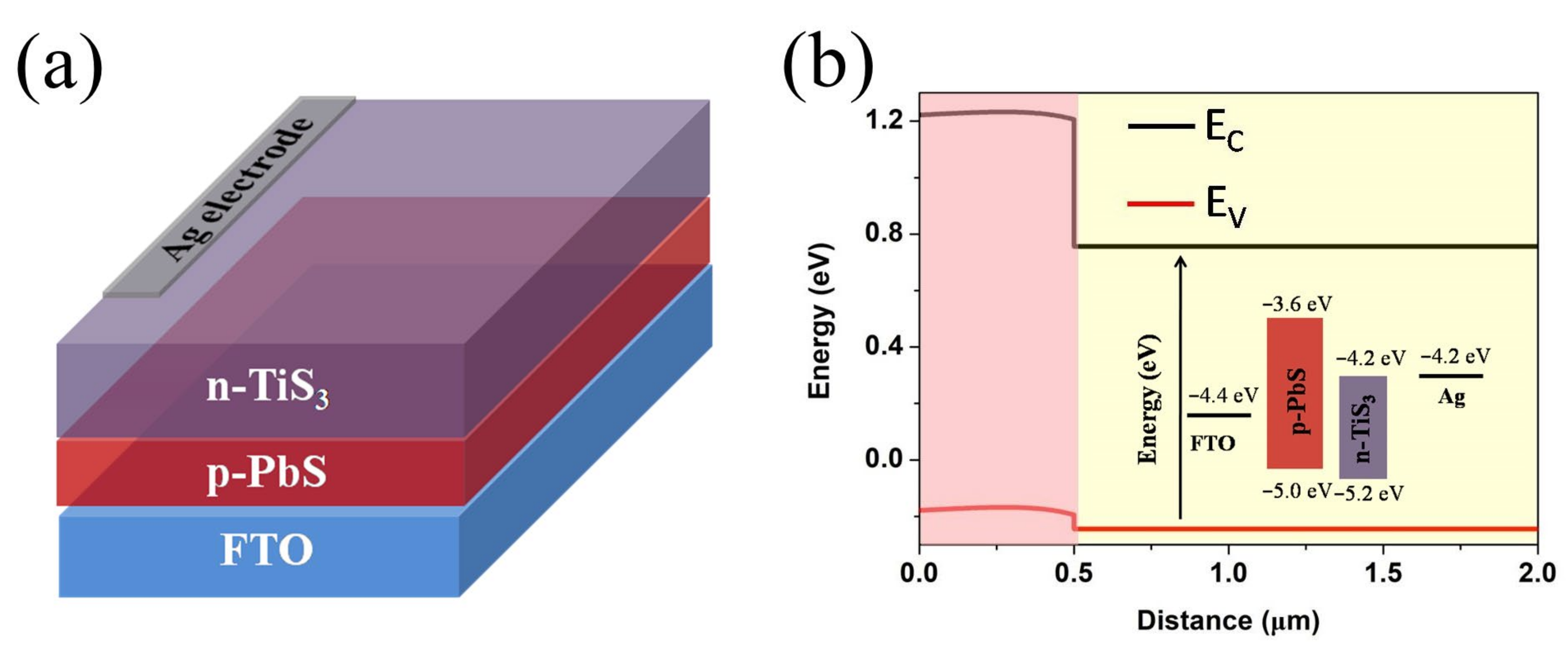
2. Numerical Simulation and Device Structure

The numerical simulation software used in this work is SCAPS-1D (V3.3.07), developed by the Department of Electronics and Information Systems of the Gent University (Ghent, Belgium) [28,29]. The software has been extensively used for simulating the thin-film solar cells to explore the electrical and optical properties, as well as the physics involved. As per previous reports, the simulated results from SCAPS have a good agreement with the experimental results [30,31]. In recent years, a number of research works based on SCAPS-1D software explored its applications in finding highly efficient photovoltaic devices [32,33,34,35,36,37]. Fundamentally, SCAPS-1D solves three sets of equations, Poisson’s equation, hole continuity, and electron continuity under the constraint of boundary conditions. These three equations are shown below [38,39,40]:
2 φ x 2 + q ε [ p ( x ) n ( x ) ρ n + ρ p N A + N D ] = 0
1 q d J p d x = G op ( x ) R ( x )
1 q d J n d x = G op ( x ) + R ( x )
where φ shows the electrostatic potential, ε is the dielectric constant, and q is the electron charge. N A is acceptor type and N D is donor type density, respectively. p ( n ) is hole (electron) concentration. ρ p ( ρ n ) is hole (electron) distribution. J p is the current densities of the hole and J n is the current densities of the electron, respectively. G op designates the optical generation rate and R is the net recombination including direct and indirect recombination. All of these parameters are the function of the position coordinate x.
The numerical modeling is an important step to understand the physical properties of, and to realize, the highly efficient photoelectronic device. The narrow band gap TiS3 layer acts as an absorber. The fluorine-doped tin oxide (FTO) layer is employed as a transparent conductive oxide layer. Figure 1a shows the diagrammatic drawing of the FTO/ PbS/TiS3/Ag thin-film heterojunction architecture photodetector. The PbS/TiS3 heterojunctions are constructed in the designed device. The energy band scheme for the PbS/TiS3 heterojunction thin-film photodetector is shown in Figure 1b. It is clearly observed that the conduction band of the PbS layer is about 0.6 eV higher compared with that of the TiS3 layer. The conduction band offset would promote photo-generated electrons towards the Ag electrode. Furthermore, the valence band maximum of the TiS3 layer is very close to that of the PbS. The estimated valance band offset is ~0.2 eV at the PbS/TiS3 interface, which would promote photo-generated holes’ transport to the FTO substrate.
The physical parameters of PbS and TiS3 layers used in this simulation are shown in Table 1. All these parameters are from previous reports and theories [12,41,42,43]. The approximate thermal velocity of electrons and holes in PbS and TiS3 semiconductor at room temperature is set at 107 cm/s for simplifying the numerical calculation. The surface recombination velocity of both electrons and holes at the FTO or Ag electrode is assumed to be 107 cm/s. The capture cross-sections of both the electron and hole are fixed at 10−14 cm2. The interface defect parameters used in the PbS/TiS3 heterojunction device simulation was 1012 cm−3. AM 1.5G illuminations is used in all of our tests to optimize the simulation investigation, using 1000 W/m2 from the PbS layer side. Photoresponsivity (R) and photodetectivity (D*) are important parameters for assessing the performance of a device and evaluate the detector sensitivity. It is assumed that the shot noise from the dark current is the primary source of total noise, R and D* are given as [44,45]:
R = I light P i n S
D * = R S 1 / 2 ( 2 e I d ) 1 / 2
where P i n is the incident light intensity, S represents the effective area of the device, and e is the elementary charge (e = 1.60 × 10⁻¹⁹ C).

3. Results and Discussion

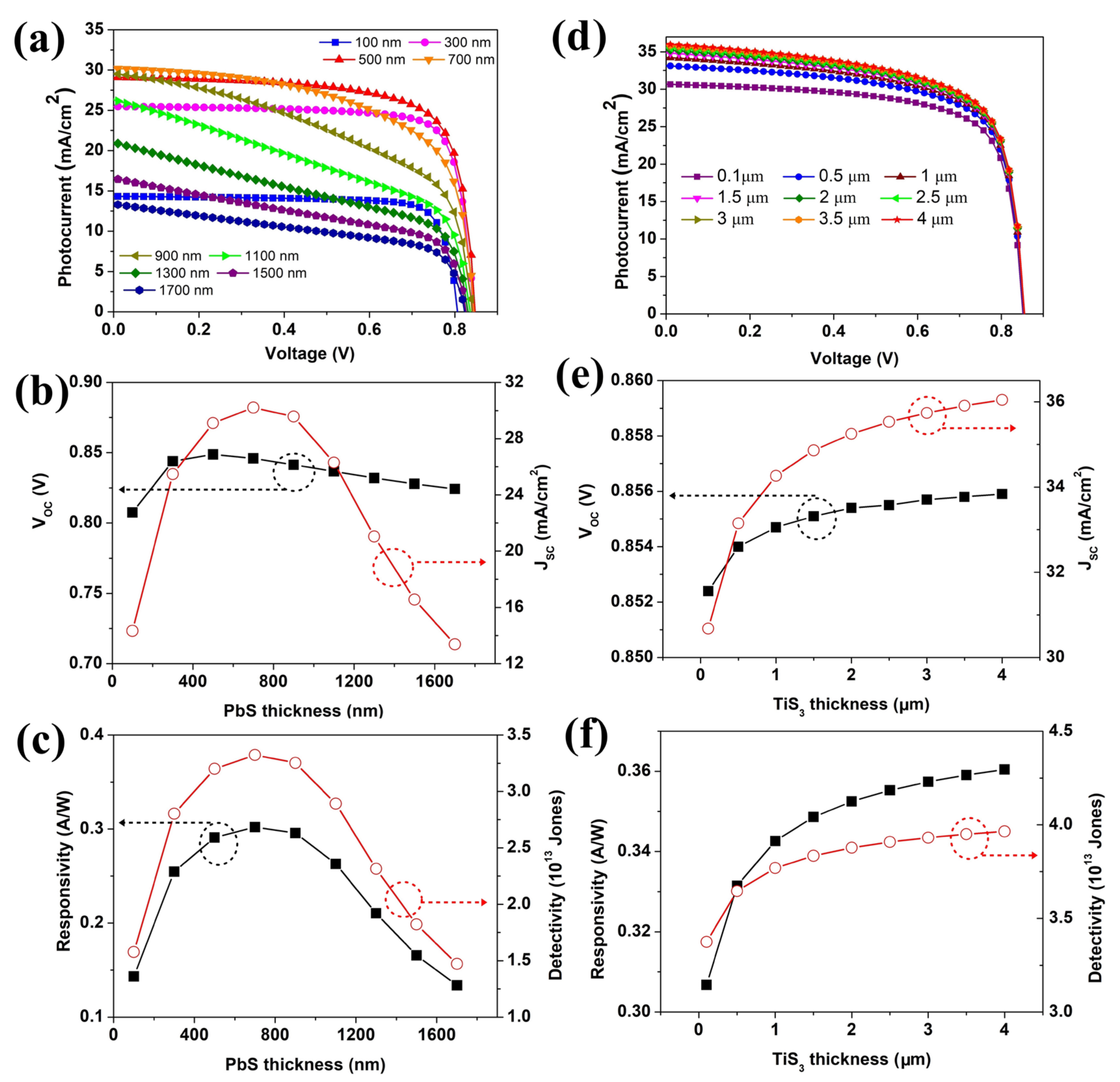
3.1. Influence of p-PbS and n-TiS3 Layer Thickness on Device Performance

The thicknesses of n-TiS3 and p-PbS layers are a key parameter to determine the performance of the detector. Optimizing the factor is in favor of obtaining optimal device performance. Figure 2 depicts the effect of the PbS and TiS3 layer thickness on the suggested photodetector performance. The PbS layer thickness was modified between 0.1–1.7 μm, while keeping the thickness of the TiS3 layer constant at 0.5 μm. As shown in Figure 2a,b, with the thickness of the PbS layer increasing from 0.1 μm to 0.7 μm, the short circuit photocurrent (JSC) obviously increased from 14.33 to 30.21 mA/cm2. This is attributed to the fact that the ultra-thin PbS layer leads to a large leakage current. However, as the thickness continues to rise to 900 nm, the JSC begins to decrease. When the thickness of the PbS layer was 1.7 μm, the JSC sharply reduced to 13.21 mA/cm2. This resulted from a large number of photons being absorbed by the PbS layer and, thus, a smaller number of photons being able to reach the junction between PbS and TiS3, which, in turn, reduced the generation of photogenerated carriers. Figure 2b shows that the variation trend of open circuit voltage (VOC) is similar to that of JSC. The appropriate thickness of the PbS layer means a higher carriers concentration, which can expand the depleted region of TiS3 and enhance the performance. When the thickness of the PbS layer was 0.7 μm, the responsitivity and detectivity were 0.3 A/W and 3.3 × 10¹³ Jones (shown in Figure 2c), respectively. The results indicate that the optimum thickness of the PbS layer is 0.7 μm.
To investigate the effect of TiS3 layer thickness, the simulation study was carried out with a thickness range from 0.1 μm to 4 μm as displayed in Figure 2d–f. It has been observed that the VOC and JSC of the simulated device were enhanced with increasing thickness of the TiS3 layer. When the thickness of the TiS3 layer was 0.1 μm, the photocurrent was 30.68 mA/cm2. The thin TiS3 layer could not fully absorb the incoming light resulting in low photocurrent while almost all of the photogenerated electron-hole could reach the corresponding electrode. As the thickness of the TiS3 layer rises, more photons are captured, resulting in a rise in JSC. The photocurrent increased to 35.53 mA/cm2 with the thickness of the TiS3 layer at 2.5 μm. Nevertheless, there was no significant change in the performance parameters when continuing to increase the thickness, resulting from the light absorption being saturated. The propagation path for the photo-generated carriers is long, leading to an increasing carrier recombination rate in the inner of TiS3 layer. The simulated device can produce a highly efficient performance when the TiS3 layer thickness is equal to 2.5 μm. The J–V characteristic curves for varying the PbS layer thickness with the constant optimized TiS3 layer at 2.5 μm are also given in Figure S1 (Supporting Information). The tendency is similar to that in Figure 2a, which verifies our conclusion. The responsivity and detectivity are 0.36 A/W and 3.9 × 10¹³ Jones (shown in Figure 2f), respectively.

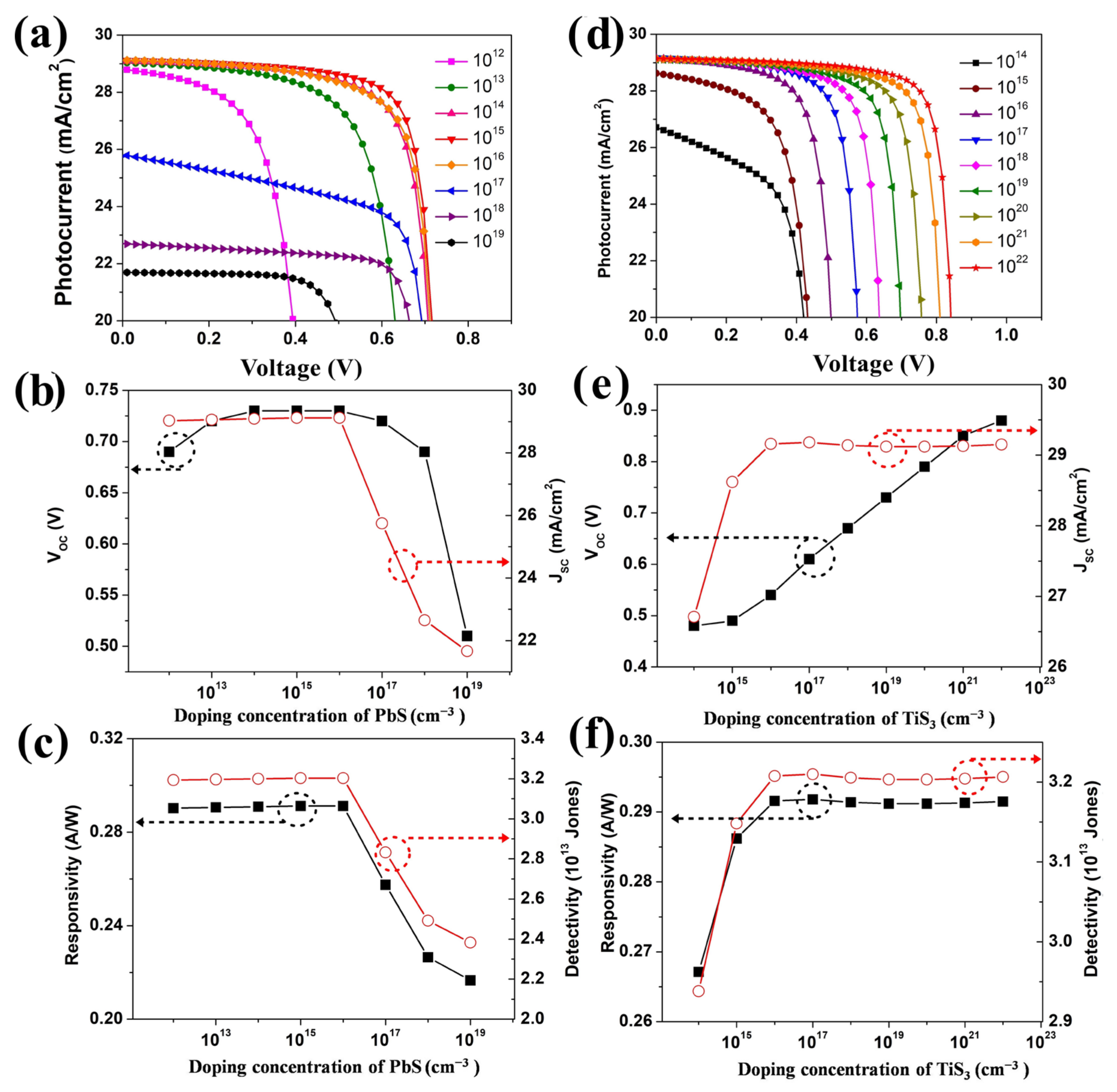
3.2. Influence of Doping Concentration of p-PbS Layer and n-TiS3 Layer

Shallow acceptor density (NA) plays an important role in improving the performance of photodetectors. In the simulation study, the doping concentration of the PbS layer was varied from 1012 cm−3 to 1019 cm−3, while other parameters remained the same. It is shown in Figure 3a,b that the VOC and JSC improves with the concentration of the PbS carrier concentration rising but below 1015 cm−3, indicating that the minority charge carrier recombination was reducing. When the doping density of the PbS layer continually increased to 1017 cm−3, the overall performance of the photodetector including JSC, VOC, responsitivity, and detectivity were quenched enormously due to the increased carriers recombination, as shown in Figure S2 (Supporting Information). It is observed in Figure 3c that the maximum responsivity and detectivity are 0.29 A/W and 3.2 × 10¹³ Jones when the acceptor density is at 1015 cm−3. The results suggest that the proper doping of the PbS layer results in a more efficient performance. As shown in Figure 3d,e, the donor density (ND) of the TiS3 layer is ranging from 1014 to 1022 cm−3. It can be observed that all the performances of the simulated photodetector were enhanced with the increasing doping density of the TiS3 layer. It is concluded that the high doping density results in a large built-in potential at the PbS/TiS3 interface. Consequently, the photo-generated carrier recombination is observably inhibited. In the numerical study, the doping concentration of 1022 cm−3 is chosen to obtain the best responsivity and detectivity (as shown in Figure 3f) of the designed photodetector.

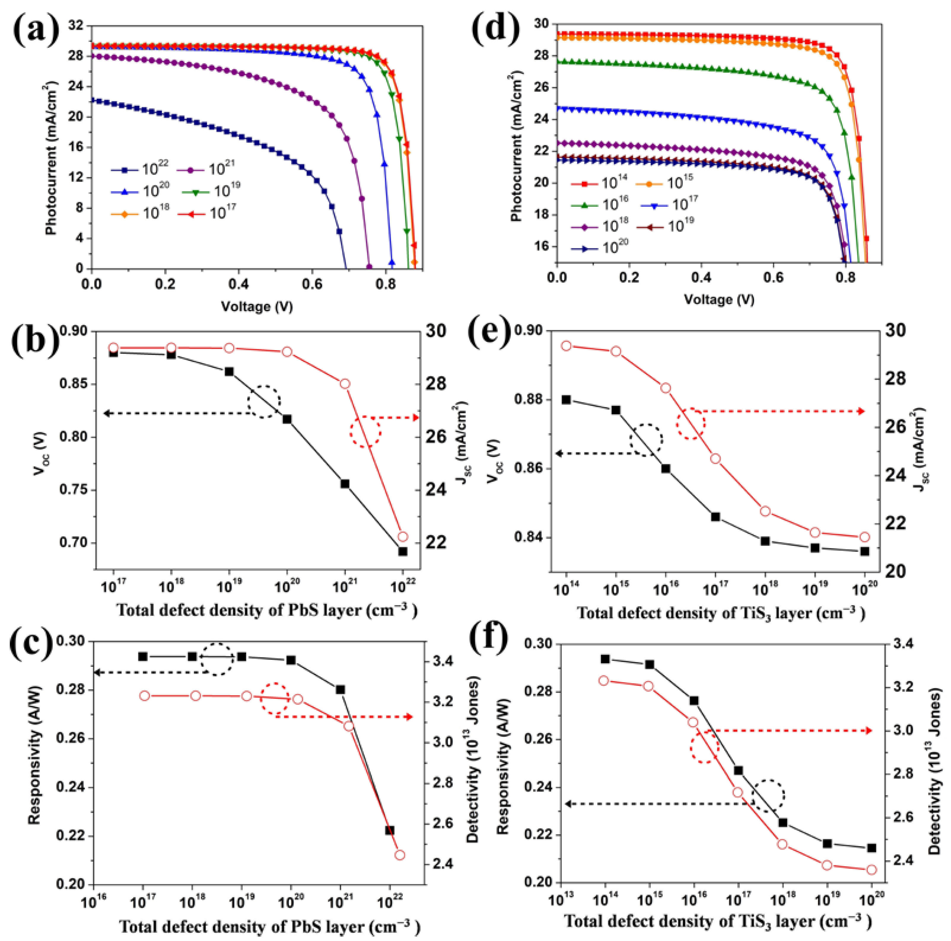
3.3. Influence of the Concentration of Defect Density

The performance of the device is also dependent on the defect density of each layer. The increase in defect density results in more photo-generated carrier recombination, which seriously reduces the efficiency of the device. In the study, the defect density of the PbS layer and TiS3 layer are varied in the range of 1012–1022 cm−3 and 1012–1020 cm−3, respectively. When the defect density of PbS was set from 1012 to 1017, shown in Figure S3 (Supporting Information), the photoelectric performance of the simulated photodetector had little change. It is seen from Figure 4a,b that, given a continuous augment in the defect density of the PbS layer, VOC and JSC are degraded. When the defect density of the PbS layer increased to 1022 cm−3, the JSC reduced to 22.24 mA/cm2 and the corresponding responsivity quenched to 0.22 A/W, as shown in Figure 4c. This is attributed to the raised carrier recombination rate with the localized energy levels created by the defects. The results show that only a mass concentration of defects in the PbS layer quenched the performance of the device. The optimal defect density of the PbS layer is ranged from 1012 to 1017. As shown in Figure S4 (Supporting Information), when the defect density of the TiS3 is ranged from 1012 to 1014, the photocurrent is kept at around 29.38 mA/cm2. When the defect density was magnified from 1014 cm−3 to 1020 cm−3, shown in Figure 4d,e, JSC varied from 29.38 mA/cm2 to 21.45 mA/cm2. It is observed from Figure 4f that responsivity and detectivity had a similar downtrend. The optimal responsivity and detectivity are 0.29 A/W and 3.2 × 10¹³ Jones, when the defect density of the PbS layer and TiS3 layer are ranged from 1012 cm−3 to 1017 cm−3 and from 1012 to 1014 cm−3.

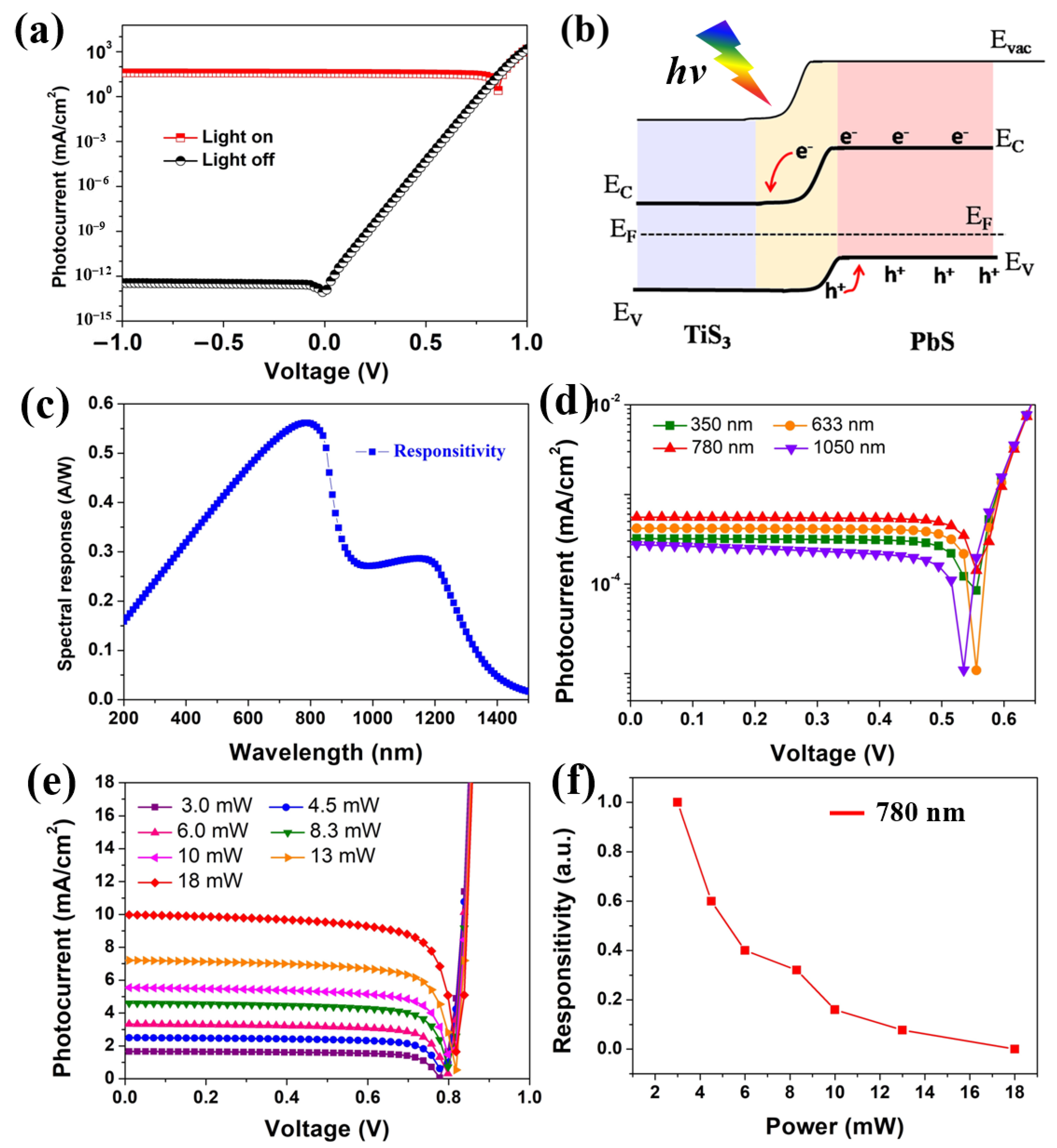
3.4. Self-Powered n-TiS3/p-PbS Heterostructure Photodetector

Through simulated optimizing, the thickness of the TiS3 layer and PbS layer are 2.5 μm and 700 nm, respectively. The density of the acceptor or donor is set at 1015 or 1022 cm−3. The high quality TiS3 film is required to have a defect density of about 1014 cm−3. For the PbS layer, the maximum defect density is 1017 cm−3. The optoelectronic performances of the simulated n-TiS3/p-PbS heterostructure devices in dark and AM 1.5G standard illuminations are shown in Figure 5a. In the dark, the photodetector displays a typical rectifying I–V characteristic due to the heterostructure formed at the interface between the n-TiS3 and the p-PbS. Under AM 1.5G illuminations, an enhanced photocurrent is observed. The photocurrent of the simulated photodetector after majorization is 35.57 mA/cm2. The optimal photoresponsivity of the proposed heterostructure device is about 0.36 A W−1 and the corresponding detectivity is 3.9 × 10¹³ Jones, which is comparable with the photodetector based on nanostructured silicon [46,47]. The ratio of light and dark current (Ilight/Idark) is about 1014 at bias voltages of 0 V. This phenomenon suggests that the photodetector can be triggered by itself. The built-in electric field which formed at the TiS3 and PbS interface can separate the photogenerated carriers even at zero bias. The photoelectrical properties displayed by the TiS3–PbS device can be clarified by the band scheme of the PbS and TiS3 materials, as displayed in Figure 5b. The band gap energies of TiS3 and PbS semiconductors are about 1.0 and 1.4 eV, respectively. As for the insulate layer, the different inherent nature leads to a different position of the Fermi levels (Supporting Information Figure S5). The electrons at the interface will be transported from the high level to the lower and, in turn, produce a potential difference at the contact interface. This phenomenon is displayed in the band scheme by the bending of the conduction and the valence band at the interface (as shown in Figure 5b). The rectifying I−V characteristics and the photovoltaic effect noticed in the proposed photodetector resulted from the type-II band mechanism. Figure 5c shows the photoresponsivity of the simulated PbS/TiS3 photodetector device. The device shows different light response characteristics under different light wavelengths. A distinct responsivity ranged from the UV to the near-infrared region is observed, which indicates the excellent broadband performance of the photodetector. With 780 nm illumination, the photodetector shows superior responsibility, as shown in Figure 5d. Figure 5e shows the I−V characteristics of the simulated device upon illumination (with 780 nm of wavelength) with enhanced optical power. It is noted that the photocurrent enhances monotonically with the augmenting light power density. This phenomenon can be a result of the growing number of photogenerated carriers as the light intensity increases. On the contrary, the responsivity decreases (Figure 5f). The R values of the photodetectors are large under low light power density, indicating that the simulated photodetectors are very sensitive to weak light.

4. Conclusions

In summary, a self-powered PbS/TiS3 heterostructure photodetector is numerically investigated. Herein, the PbS/TiS3 photodetector is modeled and optimized using SCAPS-1D software. The important parameters, including the energy bands, electron-holes generation or recombination rate, current density–voltage (J–V), and spectral response properties of the proposed device, have been explored. The influence of thickness, shallow acceptor or donor density, and defect density are also investigated. As a result, the photodetector based on the heterojunction with optimal parameters exhibits a good photoresponse from 300 nm to 1300 nm. Under AM 1.5G illuminations, the optimal short-circuit current reaches 35.57 mA/cm2 and the open circuit voltage is about 870 mV. The responsivity and a detectivity of the simulated photodetector are 0.36 A W−1 and 3.9 × 10¹³ Jones, respectively. The simulation result paves a promising way for further broadening the applicability of the TiS3-based optoelectronic device.

Supplementary Materials

The following supporting information can be downloaded at: https://www.mdpi.com/article/10.3390/nano12030325/s1, Figure S1: J–V characteristic curves for varying the PbS layer thickness with constant optimized TiS3 layer at 2.5 μm, Figure S2: Total recombination of photo carriers in the TiS3-based photodetector with varied shallow acceptor density of PbS layer, Figure S3: J–V characteristic curves for varying the PbS defect density from 1012 to 1017 cm−3, Figure S4: J–V characteristic curves for varying the TiS3 defect density from 1012 to 1014 cm−3, Figure S5: Schematic band diagram before TiS3 and PbS contacting.

Author Contributions

H.Y.: formal analysis, investigation, data curation, writing—original draft preparation. L.L.: writing—review and editing, software, visualization, supervision. All authors have read and agreed to the published version of the manuscript.

Funding

This work was financially supported by the National Natural Science Foundation of China (Grant No. 12004257) and by the Fundamental Research Program of Shanxi Province (Grant No: 20210302124397).

Acknowledgments

The authors gratefully acknowledge Marc Bargeman, University of Gent, Belgium, for providing the SCAPS simulation software.

Conflicts of Interest

The authors declare that there is no conflict of interests regarding the publication of this paper.

References

  1. Wu, Z.; Zhai, C.; Kim, H.; Azoulay, D.; Ng, N. Emerging Design and Characterization Guidelines for Polymer-Based Infrared Photodetectors. Acc. Chem. Res. 2018, 51, 3144–3153. [Google Scholar] [CrossRef] [PubMed] [Green Version]
  2. Liu, S.; Tian, J.; Wu, S.; Zhang, W.; Luo, M. A bioinspired broadband self-powered photodetector based on photo-pyroelectric-thermoelectric effect able to detect human radiation. Nano Energy 2021, 93, 106812. [Google Scholar] [CrossRef]
  3. Jiao, Y.; Lu, G.; Feng, Y.; Zhang, C.; Wang, W.; Wu, Y.; Chen, M.; Ma, M.; Li, J.; Yang, L.; et al. Towards high sensitivity infrared detector using Cu2CdxZn1-xSnSe4 thin film by SCAPS simulation. Sol. Energy 2021, 225, 375–381. [Google Scholar] [CrossRef]
  4. Clark, J.; Lanzani, G. Organic photonics for communications. Nat. Photon. 2010, 4, 438–446. [Google Scholar] [CrossRef]
  5. Zhang, J.; Itzler, M.A.; Zbinden, H.; Pan, J.-W. Advances in InGaAs/InP single-photon detector systems for quantum communication. Light Sci. Appl. 2015, 4, e286. [Google Scholar] [CrossRef] [Green Version]
  6. Tan, L.; Mohseni, H. Emerging technologies for high performance infrared detectors. Nanophotonics 2018, 7, 169–197. [Google Scholar] [CrossRef] [Green Version]
  7. Tian, W.; Wang, D.; Chen, L.; Li, L. Self-Powered Nanoscale Photodetectors. Small 2017, 13, 1701848. [Google Scholar] [CrossRef] [Green Version]
  8. Zhang, Z.; Zhang, W.; Wei, Z.; Jiang, Q.; Deng, M.; Chai, W.; Zhu, D.; Zhang, F.; You, L.; Zhang, J. Dipole-templated homogeneous grain growth of CsPbIBr2 films for efficient self-powered, all-inorganic photodetectors. Sol. Energy 2020, 209, 371–378. [Google Scholar] [CrossRef]
  9. Long, M.; Wang, P.; Fang, H.; Hu, W. Progress, challenges, and opportunities for 2D material based photodetectors. Adv. Funct. Mater. 2019, 29, 1803807. [Google Scholar] [CrossRef]
  10. Finkman, E.; Fisher, B. Electrical transport measurements in TiS3. Solid State Commun. 1984, 50, 25–28. [Google Scholar] [CrossRef]
  11. Ferrer, J.; Ares, R.; Clamagirand, M.; Barawi, M.; Sánchez, C. Optical properties of titanium trisulphide (TiS3) thin films. Thin Solid Film. 2013, 535, 398–401. [Google Scholar] [CrossRef]
  12. Dai, J.; Zeng, X. Titanium trisulfide monolayer: Theoretical prediction of a new direct-gap semiconductor with high and anisotropic carrier mobility. Angew. Chem. 2015, 127, 7682–7686. [Google Scholar] [CrossRef] [Green Version]
  13. Tripathi, N.; Pavelyev, V.; Sharma, P.; Kumar, S.; Rymzhina, A.; Mishra, P. Review of titanium trisulfide (TiS3): A novel material for next generation electronic and optical devices. Mater. Sci. Semicon. Proc. 2021, 127, 105699. [Google Scholar] [CrossRef]
  14. Li, L.; Lu, Y.; Zhang, Q.; Zhao, S.; Hu, Z.; Chou, S.L. Recent progress on layered cathode materials for nonaqueous rechargeable magnesium batteries. Small 2021, 17, 1902767. [Google Scholar] [CrossRef]
  15. Holleck, L.; Driscoll, R. Transition metal sulfides as cathodes for secondary lithium batteries—II. titanium sulfides. Electrochim. Acta 1977, 22, 647–655. [Google Scholar] [CrossRef]
  16. Ferrer, J.; Maciá, D.; Carcelén, V.; Ares, R.; Sánchez, C. On the photoelectrochemical properties of TiS3 films. Energy Procedia 2012, 22, 48–52. [Google Scholar] [CrossRef] [Green Version]
  17. Barawi, M.; Flores, E.; Ferrer, I.J.; Ares, J.R.; Sánchez, C. Titanium trisulphide (TiS3) nanoribbons for easy hydrogen photogeneration under visible light. J. Mater. Chem. A 2015, 3, 7959–7965. [Google Scholar] [CrossRef]
  18. Zhang, J.; Liu, X.; Wen, Y.; Shi, L.; Chen, R.; Liu, H.; Shan, B. Titanium trisulfide monolayer as a potential thermoelectric material: A first-principles-based boltzmann transport study. ACS Appl. Mater. Interfaces 2017, 9, 2509–2515. [Google Scholar] [CrossRef]
  19. Morozova, V.; Korobeinikov, V.; Kurochka, V.; Titov, N.; Ovsyannikov, V. Thermoelectric properties of compressed titanium and zirconium trichalcogenides. J. Phys. Chem. C 2018, 122, 14362–14372. [Google Scholar] [CrossRef]
  20. Molina-Mendoza, A.J.; Barawi, M.; Biele, R.; Flores, E.; Ares, J.R.; Sánchez, C.; Rubio-Bollinger, G.; Agraït, N.; D’Agosta, R.; Ferrer, I.J. Electronic bandgap and exciton binding energy of layered semiconductor TiS3. Adv. Electron. Mater. 2015, 1, 1500126. [Google Scholar] [CrossRef] [Green Version]
  21. Island, O.; Buscema, M.; Barawi, M.; Clamagirand, M.; Ares, R.; Sánchez, C.; Ferrer, J.; Steele, A.; Zant, J.; Castellanos-Gomez, A. Ultrahigh photoresponse of few-layer TiS3 nanoribbon transistors. Adv. Opt. Mater. 2014, 2, 641–645. [Google Scholar] [CrossRef] [Green Version]
  22. Silva-Guillén, J.A.; Canadell, E.; Guinea, F.; Roldán, R. Strain tuning of the anisotropy in the optoelectronic properties of TiS3. ACS Photon. 2018, 5, 3231–3237. [Google Scholar] [CrossRef]
  23. Liu, L.; Cheng, Z.; Jiang, B.; Liu, Y.; Zhang, Y.; Yang, F.; Wang, H.; Yu, F.; Chu, K.; Ye, C. Optoelectronic Artificial Synapses Based on Two-Dimensional Transitional-Metal Trichalcogenide. ACS Appl. Mater. Interfaces 2021, 13, 30797–30805. [Google Scholar] [CrossRef] [PubMed]
  24. Talib, M.; Tabassum, R.; Abid; Islam, S.S.; Mishra, P. Improvements in the performance of a visible–NIR photodetector using horizontally aligned TiS3 nanoribbons. ACS Omega 2019, 4, 6180–6191. [Google Scholar] [CrossRef] [Green Version]
  25. Niu, Y.; Frisenda, R.; Flores, E.; Ares, J.R.; Jiao, W.; Perez de Lara, D.; Sánchez, C.; Wang, G.; Ferrer, J.; Castellanos-Gomez, A. Polarization-Sensitive and Broadband Photodetection Based on a Mixed-Dimensionality TiS3/Si p–n Junction. Adv. Opt. Mater. 2018, 6, 1800351. [Google Scholar] [CrossRef] [Green Version]
  26. Lipatov, A.; Wilson, P.M.; Shekhirev, M.; Teeter, J.D.; Netusil, R.; Sinitskii, A. Few-layered titanium trisulfide (TiS3) field-effect transistors. Nanoscale 2015, 7, 12291–12296. [Google Scholar] [CrossRef] [Green Version]
  27. Tian, Z.; Guo, X.; Wang, D.; Sun, D.; Zhang, S.; Bu, K.; Zhao, W.; Huang, F. Enhanced charge carrier lifetime of TiS3 photoanode by introduction of S22− vacancies for efficient photoelectrochemical hydrogen evolution. Adv. Funct. Mater. 2020, 30, 2001286. [Google Scholar] [CrossRef]
  28. Soedergren, S.; Hagfeldt, A.; Olsson, J.; Lindquist, S.-E. Theoretical models for theaction spectrum and the current-voltage characteristics of microporous semiconductor films in photoelectrochemical cells. J. Phys. Chem. 1994, 98, 5552–5556. [Google Scholar] [CrossRef]
  29. Burgelman, M.; Nollet, P.; Degrave, S. Modelling polycrystalline semiconductor solar cells. Thin Solid Films 2000, 361, 527–532. [Google Scholar] [CrossRef]
  30. Huang, L.; Sun, X.; Li, C.; Xu, R.; Xu, J.; Du, Y.; Wu, X.; Ni, J.; Cai, K.; Li, J.; et al. Electron transport layer-free planar perovskite solar cells: Further performance enhancement perspective from device simulation. Sol. Energy Mater. Sol. Cells 2016, 157, 1038–1047. [Google Scholar] [CrossRef]
  31. Decock, K.; Zabierowski, P.; Burgelman, M. Modeling metastabilities in chalcopyrite-based thin film solar cells. J. Appl. Phys. 2012, 111, 43703. [Google Scholar] [CrossRef] [Green Version]
  32. He, Y.; Xu, L.; Yang, C.; Guo, X.; Li, S. Design and Numerical Investigation of a Lead-Free Inorganic Layered Double Perovskite Cs4CuSb2Cl12 Nanocrystal Solar Cell by SCAPS-1D. Nanomaterials 2021, 11, 2321. [Google Scholar] [CrossRef] [PubMed]
  33. Karthick, S.; Velumani, S.; Bouclé, J. Experimental and SCAPS simulated formamidinium perovskite solar cells: A comparison of device performance. Sol. Energy 2020, 205, 349–357. [Google Scholar] [CrossRef]
  34. Huang, C.H.; Chuang, W.J. Dependence of performance parameters of CdTe solar cells on semiconductor properties studied by using SCAPS-1D. Vacuum 2015, 118, 32–37. [Google Scholar] [CrossRef]
  35. Basak, A.; Singh, U.P. Numerical modelling and analysis of earth abundant Sb2S3 and Sb2Se3 based solar cells using SCAPS-1D. Sol. Energy Mater. Sol. Cells 2021, 230, 111184. [Google Scholar] [CrossRef]
  36. Islam, S.; Sobayel, K.; Al-Kahtani, A.; Islam, M.A.; Muhammad, G.; Amin, N.; Shahiduzzaman, M.; Akhtaruzzaman, M. Defect Study and Modelling of SnX3-Based Perovskite Solar Cells with SCAPS-1D. Nanomaterials 2021, 11, 1218. [Google Scholar] [CrossRef]
  37. Kanoun, A.; Kanoun, B.; Merad, E.; Goumri-Said, S. Toward development of high-performance perovskite solar cells based on CH3NH3GeI3 using computational approach. Sol. Energy 2019, 182, 237–244. [Google Scholar] [CrossRef]
  38. Sobayel, K.; Shahinuzzaman, M.; Amin, N.; Karim, M.R.; Dar, M.A.; Gul, R.; Alghoulg, M.A.; Sopiana, K.; Hasan, A.K.M.; Akhtaruzzaman, M. Efficiency enhancement of CIGS solar cell by WS2 as window layer through numerical modelling tool. Sol. Energy 2020, 207, 479–485. [Google Scholar] [CrossRef]
  39. Minbashi, M.; Ghobadi, A.; Ehsani, M.H.; Dizaji, H.R.; Memarian, N. Simulation of high efficiency SnS-based solar cells with SCAPS. Sol. Energy 2018, 176, 520–525. [Google Scholar] [CrossRef]
  40. Buffière, M.; Harel, S.; Guillot-Deudon, C.; Arzel, L.; Barreau, N.; Kessler, J. Effect of the chemical composition of co-sputtered Zn (O, S) buffer layers on Cu (In, Ga) Se2 solar cell performance. Phys. Stat. Solidi 2015, 212, 282–290. [Google Scholar] [CrossRef]
  41. Agarwal, A.; Qin, Y.; Chen, B.; Blei, M.; Wu, K.; Liu, L.; Shen, X.; Wright, D.D.; Green, M.D.; Zhuang, L.; et al. Anomalous isoelectronic chalcogen rejection in 2D anisotropic vdW TiS3(1−x)Se3x trichalcogenides. Nanoscale 2018, 10, 15654–15660. [Google Scholar] [CrossRef]
  42. Torun, E.; Sahin, H.; Chaves, A.; Wirtz, L.; Peeters, F.M. Ab initio and semiempirical modeling of excitons and trions in monolayer TiS3. Phys. Rev. B 2018, 98, 075419. [Google Scholar] [CrossRef] [Green Version]
  43. Chen, C.; Wang, L.; Gao, L.; Nam, D.; Li, D.; Li, K.; Zhao, Y.; Ge, C.; Cheong, H.; Song, H.; et al. 6.5% certified efficiency Sb2Se3 solar cells using PbS colloidal quantum dot film as hole-transporting layer. ACS Energy Lett. 2017, 2, 2125–2132. [Google Scholar] [CrossRef]
  44. Choi, W.; Cho, M.Y.; Konar, A.; Lee, J.H.; Cha, G.B.; Hong, S.C.; Kim, S.; Kim, Y.; Jena, D.; Joo, J.; et al. High-detectivity multilayer MoS2 phototransistors with spectral response from ultraviolet to infrared. Adv. Mater. 2012, 24, 5832–5836. [Google Scholar] [CrossRef]
  45. Binda, M.; Iacchetti, A.; Natali, D.; Beverina, L.; Sassi, M.; Sampietro, M. High detectivity squaraine-based near infrared photodetector with nA/cm2 dark current. Appl. Phys. Lett. 2011, 98, 073303. [Google Scholar] [CrossRef]
  46. Yu, H.; Shu, S.; Xiong, X.; Xie, Q. Simulation design and performance study of Graphene/Mg2Si/Si heterojunction photodetector. Appl. Phys. A 2021, 127, 548. [Google Scholar] [CrossRef]
  47. Wu, E.; Wu, D.; Jia, C.; Wang, Y.; Yuan, H.; Zeng, L.; Xu, T.; Shi, Z.; Tian, Y.; Li, X. In situ fabrication of 2D WS2/Si type-II heterojunction for self-powered broadband photodetector with response up to mid-infrared. ACS Photon. 2019, 6, 565–572. [Google Scholar] [CrossRef] [Green Version]
Figure 1. (a) Schematic n-TiS3/p-PbS heterostructure photodetector, (b) energy band scheme of PbS/TiS3 heterojunction.
Nanomaterials 12 00325 g001
Figure 2. (a) J–V characteristic curves for varying the PbS layer thickness, (b) VOC and JSC variation, (c) R and D* variation with respect to the thickness of the PbS layer, (d) J–V characteristic curves for varying the TiS3 layer thickness, (e) VOC and JSC variation, (f) R and D* variation with respect to the thickness of the TiS3 layer.
Nanomaterials 12 00325 g002
Figure 3. (a) J–V characteristic curves, (b) VOC and JSC variation, (c) R and D* variation for varying the PbS shallow acceptor density, (d) J–V characteristic curves, (e) VOC and JSC variation, (f) R and D* variation for varying the TiS3 shallow donor density.
Nanomaterials 12 00325 g003
Figure 4. (a) J–V characteristic curves for varying the PbS defect density, (b) VOC and JSC variation, (c) R and D* variation with respect to the PbS defect density of the PbS layer, (d) J–V characteristic curves for varying the TiS3 defect density, (e) VOC and JSC variation, (f) R and D* variation with respect to the defect density of the TiS3 layer.
Nanomaterials 12 00325 g004
Figure 5. (a) I–V curves of the simulated photodetector with and without light illumination, (b) schematic band diagram after contacting, (c) responsivity with different illumination wavelengths at a power of 100 mW/cm2, (d) I−V characteristics of simulated PbS/TiS3 under different wavelengths of illumination and (e) illuminated with a 780 nm wavelength at different powers, (f) dependence of responsitivity of the photodetector versus the light illumination power.
Nanomaterials 12 00325 g005
Table 1. Parameters set for the simulation of TiS3-based photodetector.
PropertiesFTOPbSTiS3
Thickness (nm)300200500
Band gap (eV)3.61.41.0
Electron affinity (eV)4.04.354.8
Dielectric permittivity (relative)9.0109.98
Electron thermal velocity (cm/s)1 × 1071 × 1071 × 107
Hole thermal velocity (cm/s)1 × 1071 × 1071 × 107
CB effective DOS (cm−3)2.2 × 10181 × 10181 × 1018
VB effective DOS (cm−3)1.8 × 10191 × 10181.8 × 1019
Donor density ND (cm−3)1 × 101701 × 1018
Acceptor density NA (cm−3)01 × 10170
Electron Mobility (cm2/Vs)10050200
Hole mobility (cm2/Vs)251094
Publisher’s Note: MDPI stays neutral with regard to jurisdictional claims in published maps and institutional affiliations.

