Article

Study on the Electrical Conduction Mechanism of Unipolar Resistive Switching Prussian White Thin Films

by
Lindiomar B. Avila
1,*,
Pablo C. Serrano Arambulo
1,
Adriana Dantas
2,
Edy E. Cuevas-Arizaca
3,
Dinesh Kumar
4 and
Christian K. Müller
5,*
1
Departamento de Física, Universidade Federal de Santa Catarina, Florianópolis 88040-900, Santa Catarina, Brazil
2
Department of Chemical and Food Engineering, Federal University of Santa Catarina, Florianopolis 88040-900, Santa Catarina, Brazil
3
Universidad Católica de Santa Maria, Arequipa 04000, Perú
4
Shoolini University of Biotechnology and Management Sciences, Solan 173229, India
5
Faculty of Physical Engineering/Computer Sciences, University of Applied Sciences Zwickau, 08056 Zwickau, Germany
*
Authors to whom correspondence should be addressed.
Nanomaterials 2022, 12(16), 2881; https://doi.org/10.3390/nano12162881
Submission received: 8 July 2022 / Revised: 4 August 2022 / Accepted: 10 August 2022 / Published: 22 August 2022
(This article belongs to the Section Nanoelectronics, Nanosensors and Devices)

Abstract

:
The electrical conduction mechanism of resistive switching Prussian white (PW) thin films obtained by the electrodeposition method was examined by AC impedance spectroscopy and DC current–voltage measurements. Using an electrode tip to contact PW grown over Au, robust unipolar resistive switching was observed with a current change of up to three orders of magnitude, high repeatability, and reproducibility. Moreover, electrical impedance spectroscopy showed that the resistive switching comes from small conductive filaments formed by potassium ions before the establishment of larger conductive channels. Both voltammetry and EIS measurements suggest that the electrical properties and conductive filament formation are influenced by defects and ions present in the grain boundaries. Thus, PW is a potential material for the next generation of ReRAM devices.

Graphical Abstract

1. Introduction

One of the biggest challenges that the electronic devices industry is facing is the requirements of less power consumption, less latency, higher density, higher bandwidth, and lower cost, leading to the development of alternatives such as ReRAMs [1,2]. ReRAMs are considered potential candidates for the next generation of non-volatile memories since they offer high switching speed, simple cell structure, small cell size, high durability, and multistate switching [3,4]. Various types of materials for ReRAM have been proposed, such as transition-metal oxides, perovskite-structured ceramics, and highly insulating oxides including N i O , T i O 2 , Z n O , C r -doped S r Z O 3 , and S r T i O 3 [5,6,7]. In this sense, finding new materials that are environmentally friendly and have low cost is an important challenge.
Generally, ReRAMs are simple two-terminal devices, forming a metal–insulator–metal (MIM) structure that shows resistive switching, referred as a memristor. Although resistive switching was observed in the mid-1960s on several devices built in the MIM format [8,9], the theoretical modeling of memristors was described in the 1970s [10], and only in 2008, devices were reported [11].
Regarding the RS effect, the switching can be classified into two types: bipolar (BRS) and unipolar (URS). In addition to the intricate parameters of each material, other factors that can determine the type are the current and potential limitation window [12,13].
Prussian blue analogs (PBAs) are a class of materials with high potential for ReRAMs. The growth of Prussian blue analog (PBA) films has been successfully achieved by electrodeposition [14], liquid-phase epitaxy [15], and spin coating [16]. Among them, electrodeposition is a very effective method for the growth of thin PBA films on a solid substrate due to its high reproducibility, low cost, and ease of controlling deposition parameters (e.g., deposition rate, film thickness, morphology) [14]. Prussian blue (PB) and Prussian white (PW) belong to PBAs. PW is a ferrocyanide complex K x F e 2 + [ F e 2 + ( C N ) y ] ; the differences between PB and PW are the oxidation state of Fe ions bound to nitrogen atoms and the insertion of potassium atoms in the structure [17,18,19,20,21].
However, the electrical properties of PBA films are rarely investigated. In previous works, characterizations were presented for Prussian blue (PB) and Prussian white (PW) thin films that showed the behavior of bipolar resistive switching (BRS) and unipolar resistive switching (URS) types, respectively. The samples showed excellent stability of up to 500 cycles and an ON/OFF ratio of three orders of magnitude, with strong evidence that the conductive mechanism occurs in metallic filaments due to the migration of K ions to one of the interfaces [22,23].
The present work shows that electrodeposited PW films can have unipolar resistive switching behavior. By the defined variation of electrical parameters and by studying the PW films with electrical impedance spectroscopy, a deeper analysis of the unipolar resistive switching characteristics and the underlying conduction mechanism is obtained.

2. Experimental Section

2.1. Material Preparation

The electrochemical deposition of the PW films was performed in potentiostatic mode using an electrochemical workstation (Ivium CompactStat, Eindhoven, Netherlands), at room temperature by using Au/Cr/Si substrates as working electrodes, a Pt foil as a counter electrode, and a saturated calomel electrode (SCE) as reference (Figure 1a). All the voltages in the text refer to this reference electrode. The working electrode was prepared by evaporating 50   n m Au on 5   n m   C r on (100) Si substrates with a size of 1   c m × 1   c m at a base pressure of 10 5 Pa (Figure 1b). The deposition of PW occurred in a circular area of 0.5   c m 2 defined by a mask of adhesive tape on the surface of the working electrode. As electrolyte for the electrochemical synthesis, a solution of 0.25   m M   K 3 F e ( C N ) 6 , 0.25   m M   F e C l 3 , 1.0   M   K C l , and 5.0   m M   H C l   at pH 2 was used [24]. All chemicals used were of high purity, >99%, (Sigma Aldrich, Darmstadt, Germany). The PW layers were deposited by applying a constant potential of 0.1   V at 25 °C and limiting the electrodeposited charge to 30   m C .

2.2. Characterization

The morphology of the PW films was investigated with a TESCAN field emission scanning electron microscope (FEG-SEM, TESCAN CLARA, Brünn, Czech Republic) at 10 kV.
Electrical characterization (current vs. voltage ( I × V )), was performed on electrodeposited samples using an electrochemical workstation (Ivium CompactStat, Eindhoven, Netherlands) with a d c voltage ranging from 1   t o + 1   V . For the electrical measurements, a 2-point probe was used with one contact at the top of the PW film using a metallic tip with surface area of 0.5   m m 2 and the Au on bottom layer (Figure 1b). Electrochemical impedance spectroscopy (EIS) was performed in an impedance analyzer (Agilent 4294A, Santa Clara, CA, USA) operating in the frequency range between 40   H z and 100   M H z . The applied potentials were AC V R M S   of 100 mV and fixed DC bias voltages of 0.5   V ,   1.5   V , and 2.0   V .

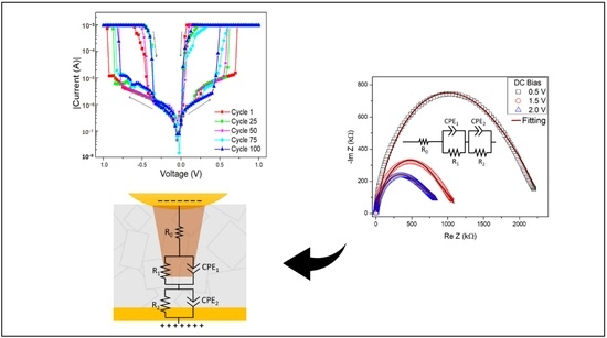
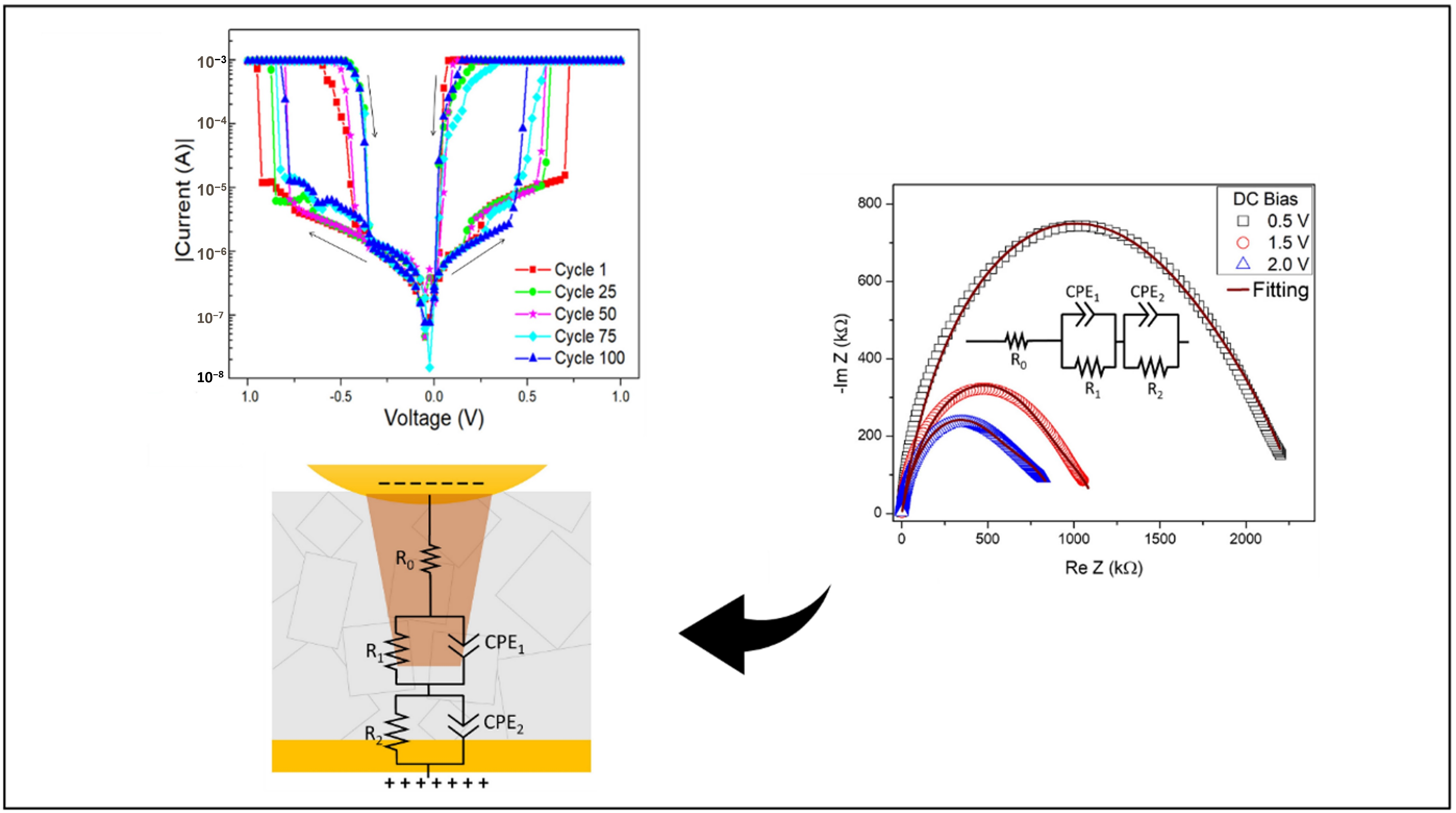
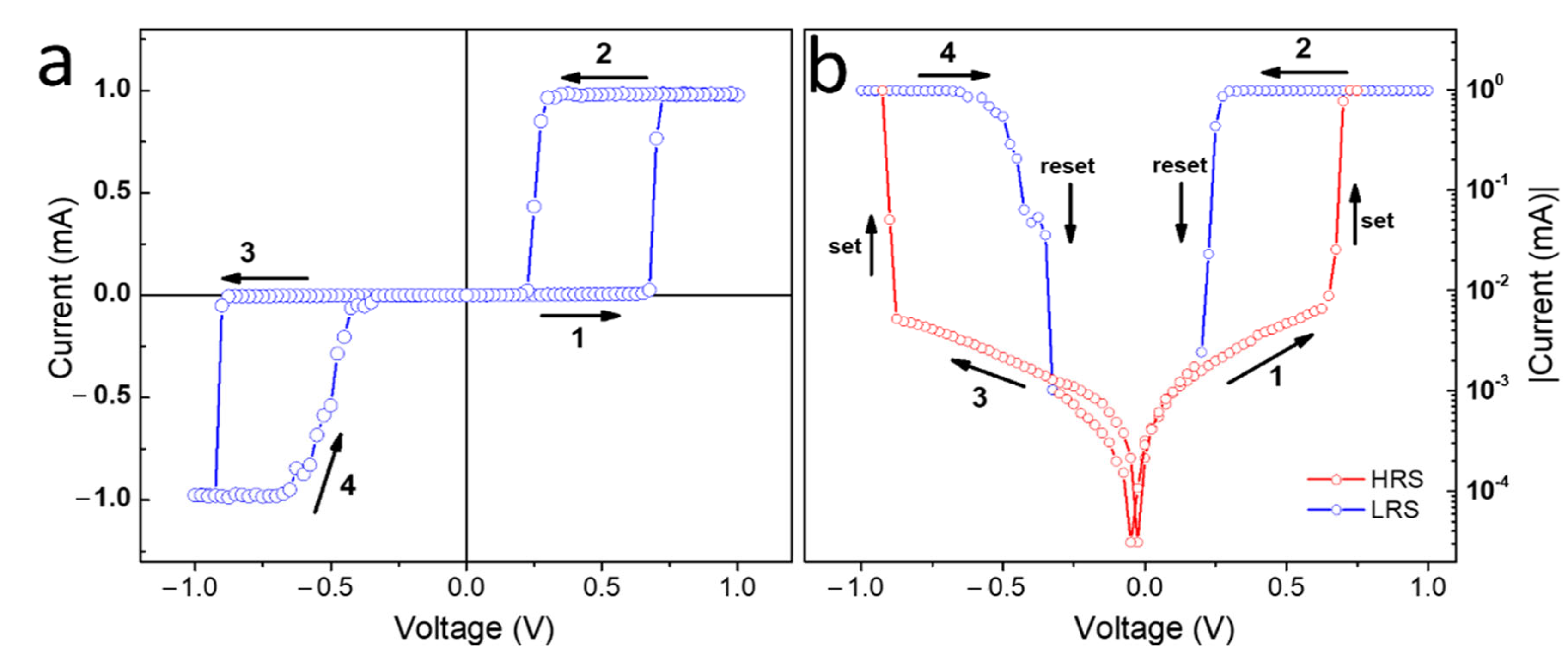
3. Results and Discussion

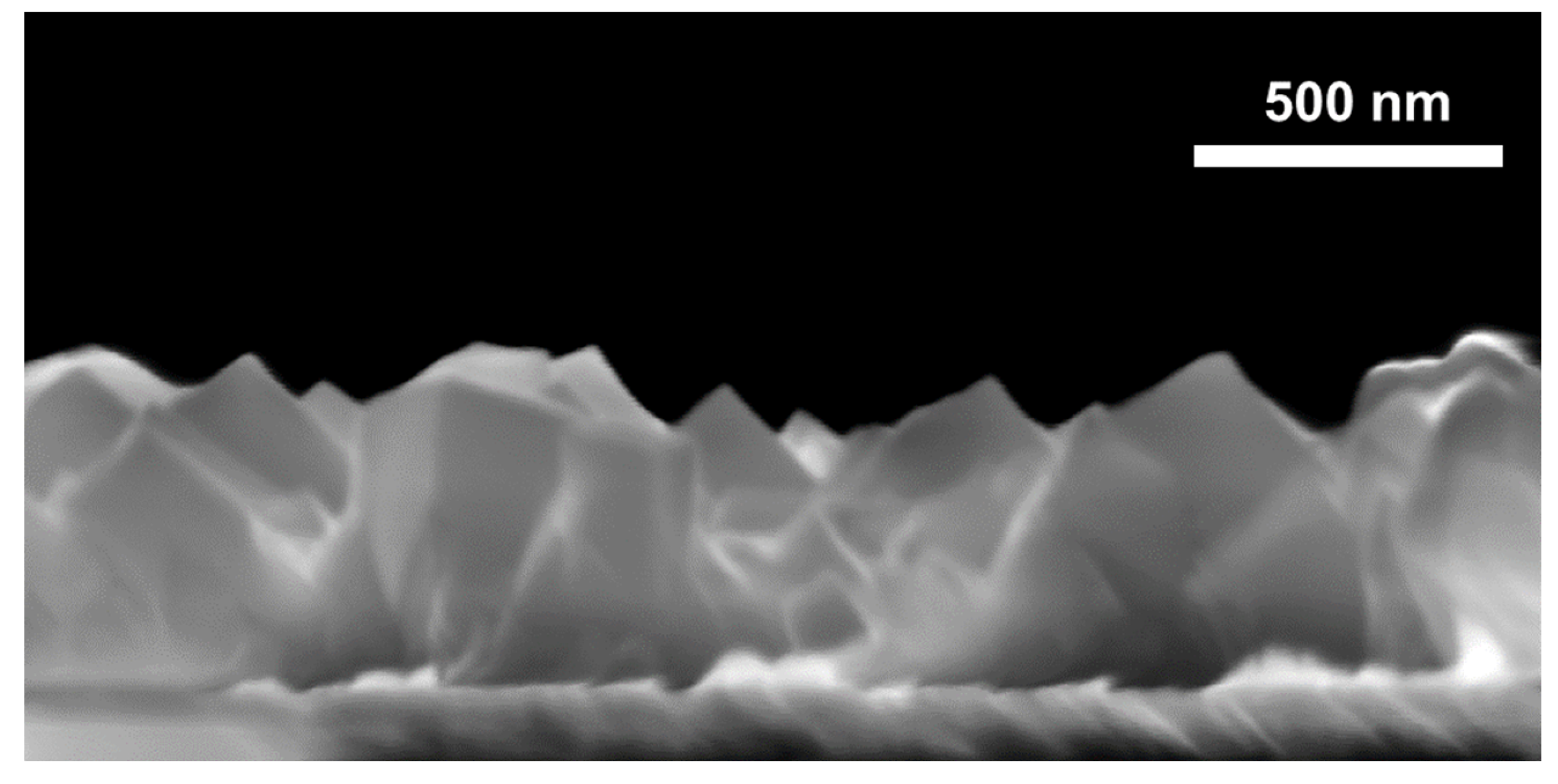
3.1. Morphological Characterization

Figure 2 shows a cross-section image of the PW film. From the electron microscopy image, an average film thickness of about 500 nm can be determined. Surface analysis of the PW film with atomic force microscopy (not shown) gave an average peak-to-valley height of approximately 100 nm. The morphology with different grains is visible along the whole layer and shows cubes along the layer thickness. The preferential growth direction of the majority of the cubes is [111]. Generally, the grains near the bottom are significantly smaller in size than the grains at the top. Such a grain distribution and the appearance of cubes typically occurs by the Volmer–Weber growth process, where three-dimensional islands are formed on the substrate surface and then grow in sequence until they coalesce into a continuous film. Our films prove that a good control of film thickness, morphology, and structure can be achieved by electrodeposition. This result makes electrodeposition attractive against other film deposition methods, such as spin coating or liquid-phase epitaxy.

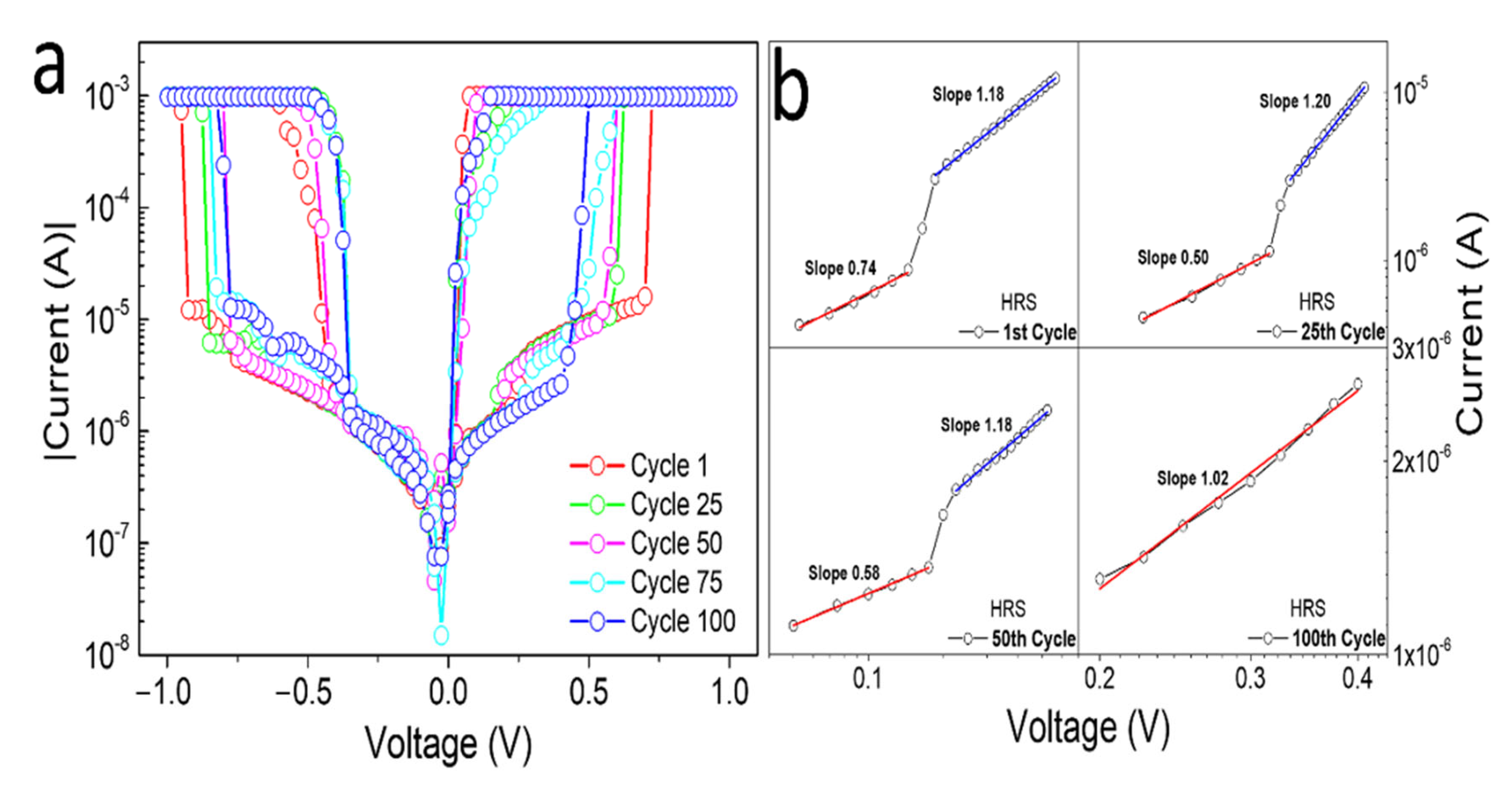
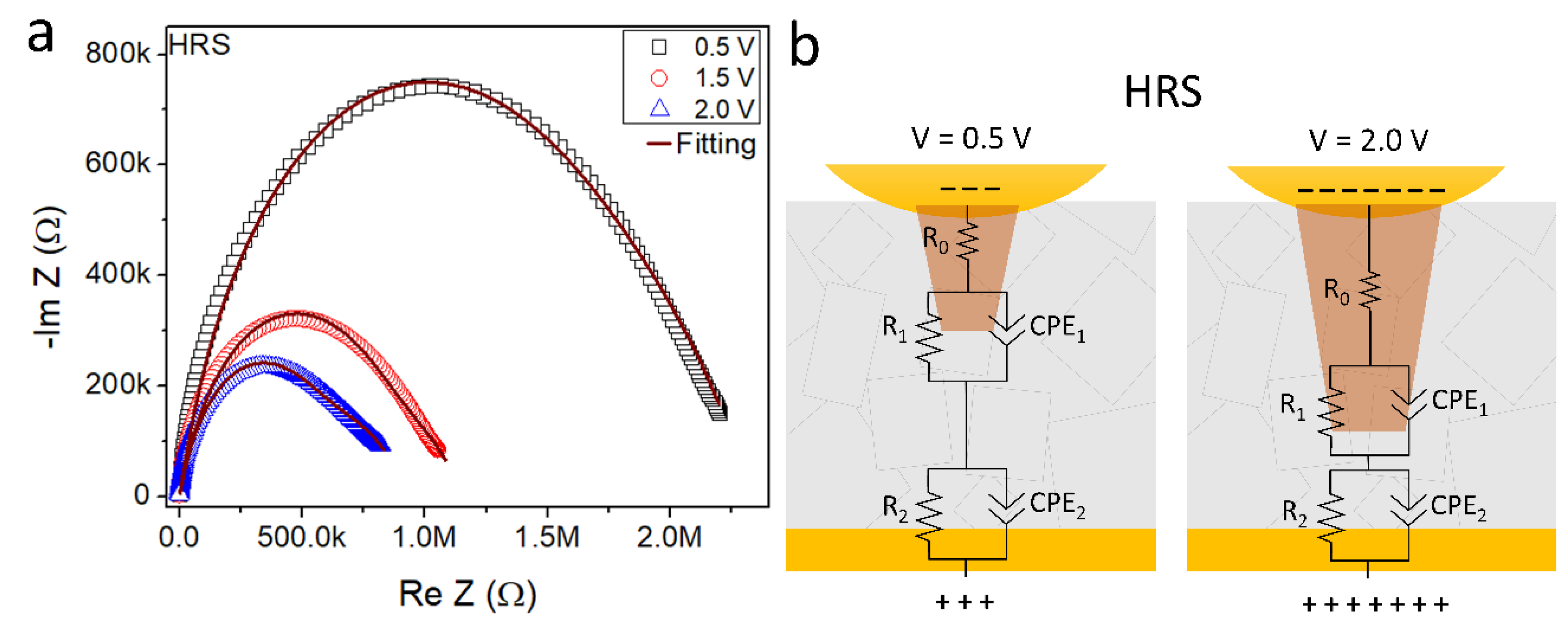
3.2. Electrical Characterization

Figure 3a shows the result of the electrical measurement in a sandwich structure with the Au layer as bottom contact and a metallic tip as top contact. The voltammetry was performed between 1   and   1   V . The current was limited to 1   m A to avoid damage [25,26,27]. In the bias voltage between 0 and 1.0   V , the high-resistance state (HRS), off state, switches at 0.7   V (step 1 ) to the low-resistance state (LRS), the on state. The LRS is maintained up to 1.0   V and is reset into HRS at 0.3   V when the current abruptly decreases (step 2 ), back to the off state. Similar behavior is observed in the negative-bias region, where the switch occurs at around 0.9   V (step 3 ) and the resetting at 0.4   V (step 4 ). The resistive switching at the same potential that occurs in the PW films is characteristic for unipolar resistive switching (URS) [28]. Figure 3b presents the same I × V curve on a semi-logarithmic scale showing a current switch greater than three orders of magnitude for both polarities. The curve clearly exhibits a characteristic butterfly shape or the pinched hysteresis characteristics of resistive switching devices [28,29].
The repeatability of the working resistive switching over one hundred cycles is shown in Figure 4a. The on/off ratio between the LRS and HRS states remained around three orders of magnitude in current even after 100 cycles, and the URS effect was preserved for both polarities. This result confirms the reversibility and reproducibility of the PW films required for applications in ReRAM memory devices. In comparison with other materials showing the resistive switching effect reported in the literature (in most cases oxides), we found typical switching ratios in the range from 10 to 106 and endurances in the range from 1 up to 107 [30]. However, it is important to note that most of the studied materials show values comparable with our PW samples. The conduction mechanism that occurs in the PW thin film was analyzed in the HRS (off state) and positive-bias region, as shown in Figure 4b. The   I × V   curves of the 1 st ,   25 th ,   50 th , and 100 th scans were plotted with a log–log scale and the data were fitted. For the lower applied field at HRS region, up to around 0.3 V , the slope values varied between 0.5 and 0.74 indicating a high resistive state. Further increment in the applied electric field caused a gradual increment in the slopes close to one with increasing number of cycles, indicating a linear ohmic behavior (I ∝ V) and the formation of small conductive metallic filaments between the top and down electrodes, still in the HRS region [31,32,33,34,35]. Higher slopes with values closer to two can be an indication for a space charge limited current (SCLC) mechanism following a quadratic relationship between voltage and current [36]. However, in our samples, SCLC was not the dominating effect in the investigated voltage range.
To elucidate the electrical response of our samples to the electric field, different voltage scan rates were applied, without increasing the potential range to avoid damage to the PW film. Figure 5a shows the electrical response in the positive-bias range for the system with voltage scan rates of 100 , 50 , 15 , and 0.5   m V / s . Notice that the resistivity switching effect is preserved, but a shift of the setting potential ( V s e t ) occurs. As expected, when the scan speed decreases, the V s e t also decreases due to the increased time in which the PW is stimulated by the external potential. The inset in Figure 3a shows the relation of V s e t and voltage scan rate.
Figure 5b presents the HRS state for different scan rates on the log–log scale. The angular coefficients for the different voltage scan rates were around 1.17   ±   0.07 , indicating an ohmic behavior for the high-resistance state at lower scan rates. At higher potentials, larger filaments are formed, which are responsible for the strong change in the electrical current observed in the film. The filament model suggests that the filaments are composed and formed from defects such as vacancies or metal ions [31]. PW films are rich in potassium ions, and our data strongly support a mechanism based on the generation of filaments induced by the migration of these cations during the formation process, as indicated in Figure 5c. When applying a bias voltage, the positively charged potassium ions can move to the negative pole (top or bottom depending on the polarity). At applied voltages larger than V s e t , the formation of a conductive path can occur, and the resistance drops. According to the filament model [32], the defect lines form tiny conductive filaments in the HRS, and these filaments come together to form larger and more conductive filaments, leading to the transition to the LRS. Defects, grain boundaries, and lattice distortion provide easy diffusion paths for ions, thus forming conduction paths. The results presented here agree with earlier findings obtained from Prussian blue (PB) and Prussian white (PW) thin films [22,23], which indicated that the filamentary conduction mechanism can explain the huge resistance change in those films.
Thus far, the conductive channels formed by the migration of potassium have not been proven, but the results presented in this work show strong evidence of how and where changes in the material arise upon the application of an external electric field. This hypothesis is due to the fact that thin PW films are potassium rich and these ions are the only free ions in the crystalline lattice and grain boundaries to cause the RS effect.
For further clarification of the underlying electrical transport mechanism in the PW film, electrical impedance spectroscopy was used. Figure 6 shows the Nyquist plot as well as a schematic diagram of the intermediary filament formation and the respective equivalent circuits used to fit the curves.
The three Nyquist diagrams show single semicircles fitted by two constant-phase elements ( C P E 1 and C P E 2 ) in parallel with the resistances R 1 and R 2 . C P E s are assigned to the interfaces filament/PW film and PW film/Au electrode that behave as double layers, as shown in Figure 6b. At high frequencies, R 2 / / C P E 2 is assigned to interface the Au/PW film and the charge transport in the PW crystals, while at lower frequencies, R 1 / / C P E 1 is assigned to charge transport on the interface filament/grain boundary defects with traps and charge accumulation [37,38,39,40,41,42,43].
The curves show that lower impedances at high frequencies (left end of the curves) may be explained by Koop’s theory, which assumes that the conductive grains are separated by resistive layers of grain boundaries [44]. In our case, the PW crystals are the grains involved by grain boundaries. The high impedances at lower frequencies (right end of the curves) are related to grain boundaries.
The series resistance ( R 0 ) present in all circuits shows larger values for higher DC biases: R0 = 173.8, 270.2, and 331.3 Ω for bias 0.5, 1.5, and 2.0 V, respectively. These results strongly indicate the formation/increment of small metallic conductive filaments between both electrodes [45]. On the other hand, as the impedance module is reduced for larger DC bias, and the parallels R / C P E s under 1.5 and   2.0   V present lower impedance values, compared to ones from 0.5 V bias.
The impedance results suggest that the electrical responses are mainly influenced by the formation of conductive filaments, most possibly at the grain boundaries and different interfaces (film/electrodes), in agreement with literature results [22,37,38,39,40,41,42,43] and electrical characterization at DC measurements. The interfaces and respective R / / C P E circuits are hypotheses as the physico-chemical origin of such C P E behavior at these interfaces is not yet fully understood [46]. Heterogeneities on the interface have been suggested to lead to a distribution of charge accumulation time scales, due to different times of charge carrier relaxation in these materials, as given by the Maxwell–Wagner two-layer model, in agreement with Koop’s phenomenological theory [37].

4. Conclusions

We observed the resistive switching mechanism in electrodeposited layers of Prussian white. The PW films showed a unipolar switching effect with an on/off current ratio of up to three orders of magnitude and good reproducibility of 100 cycles. The electrical measurements show the rise of the ohmic conduction model in the HRS region that suggests the formation of small conductive filaments before the establishment of larger conductive channels for setting the film into the LRS. Both voltammetry and EIS measurements suggest that the electrical properties and conductive filaments formed in the films are determined by the influence of defects and ions present on the grain boundaries. This recent discovery strongly indicates that the conduction channels are formed by potassium ions, the most credible for the resistive switching effect in PW films. This result opens further possibilities such as ionic control in the interstices of PW by using an external electric field and ensuring that the material does not degrade with time and use. However, to access practical applications of PW as next-generation ReRAM devices, the electrical switching characteristics, influence of fabrication parameters, long-time behavior, and impact of environmental conditions need to be carefully studied in future works.

Author Contributions

Validation—L.B.A., P.C.S.A., A.D. and C.K.M.; formal analysis—L.B.A., P.C.S.A., A.D. and C.K.M.; investigation—L.B.A. and C.K.M.; writing—original draft preparation—L.B.A., E.E.C.-A. and C.K.M.; writing—review and editing—L.B.A. and C.K.M.; funding—D.K. and C.K.M.; conceptualization, methodology, supervison—C.K.M. All authors have read and agreed to the published version of the manuscript.

Funding

L.B.A. thanks DAAD for funding (project 249302).

Acknowledgments

L.B.A. acknowledge Miguel Boratto for the initial guidance on the effect of RS.

Conflicts of Interest

The authors declare that they have no known competing financial interest or personal relationships that could have appeared to influence the work reported in this paper.

References

  1. Ling, Q.; Song, Y.; Ding, S.J.; Zhu, C.; Chan, D.S.H.; Kwong, D.-L.; Kang, E.-T.; Neoh, K.G. Non-Volatile Polymer Memory Device Based on a Novel Copolymer ofN-Vinylcarbazole and Eu-Complexed Vinylbenzoate. Adv. Mater. 2005, 17, 455–459. [Google Scholar] [CrossRef]
  2. Hamann, H.F.; O’Boyle, M.; Martin, Y.C.; Rooks, M.; Wickramasinghe, H.K. Wickramasinghe Ultra-high-density phase-change storage and memory. Nat. Mater. 2006, 5, 383–387. [Google Scholar] [CrossRef]
  3. Gaba, S.; Knag, P.; Zhang, Z.; Lu, W. Memristive devices for stochastic computing. In Proceedings of the 2014 IEEE International Symposium on Circuits and Systems (ISCAS), Melbourne, Australia, 1—5 June 2014; Volume 8, pp. 2592–2595. [Google Scholar] [CrossRef]
  4. Prezioso, M.; Hoskins, B.D.; Adam, G.C.; Likharev, K.K.; Strukov, D.B. Training and operation of an integrated neuromorphic network based on metal-oxide memristors. Nature 2015, 521, 61–64. [Google Scholar] [CrossRef] [Green Version]
  5. Choi, J.S.; Park, B.H. Reproducible resistance switching in polycrystalline NiO films. Appl. Phys. Lett. 2006, 85, 5655–5657. [Google Scholar] [CrossRef]
  6. Choi, D.; Lee, D.; Sim, H.; Chang, M.; Hwang, H. Reversible resistive switching of thin films for nonvolatile memory applications. Appl. Phys. Lett. 2005, 88, 082904. [Google Scholar] [CrossRef]
  7. Song, S.J.; Kim, K.M.; Kim, G.H.; Lee, M.H.; Seok, J.Y.; Jung, R.; Hwang, C.S. Identification of the controlling parameter for the set-state resistance of a TiO2 resistive switching cell. Appl. Phys. Lett. 2010, 96, 112904. [Google Scholar] [CrossRef]
  8. Simmons, J.G.; Verderber, R.R. New Thin-film Resistive Memory. Radio Electron. Eng. 1967, 34, 81–89. [Google Scholar] [CrossRef]
  9. Hickmott, T.W. Low-Frequency Negative Resistance in Thin Anodic Oxide Films. J. Appl. Phys. 1962, 33, 2669–2682. [Google Scholar] [CrossRef]
  10. Chua, L. Memristor-The missing circuit element. IEEE Trans. Circuit Theory 1971, 18, 507–519. [Google Scholar] [CrossRef]
  11. Strukov, D.B.; Snider, G.S.; Stewart, D.R.; Williams, R.S. The missing memristor found. Nature 2008, 453, 80–83. [Google Scholar] [CrossRef]
  12. Luo, J.M.; Lin, S.P.; Zheng, Y.; Wang, B. Nonpolar resistive switching in Mn-doped BiFeO3 thin films by chemical solution deposition. Appl. Phys. Lett. 2012, 101, 062902. [Google Scholar] [CrossRef]
  13. Boratto, M.H.; Ramos, R.A.; Congiu, M.; Graeff, C.F.; Scalvi, L.V. Memristive behavior of the SnO2/TiO2 interface deposited by sol—gel. Appl. Surf. Sci. 2017, 410, 278–281. [Google Scholar] [CrossRef]
  14. Baggio, B.F.; Vicente, C.; Pelegrini, S.; Cid, C.C.P.; Brandt, I.S.; Tumelero, M.A.; Pasa, A.A. Morphology and Structure of Electrodeposited Prussian Blue and Prussian White Thin Films. Materials 2019, 12, 1103. [Google Scholar] [CrossRef] [Green Version]
  15. Lei, S.; Li, Q.-.Q.; Kang, Y.; Gu, Z.-.; Zhang, J. Epitaxial growth of oriented prussian blue analogue derived well-aligned CoFe2O4 thin film for efficient oxygen evolution reaction. Appl. Catal. B Environ. 2019, 245, 1–9. [Google Scholar] [CrossRef]
  16. Wang, Z.; Nminibapiel, D.; Shrestha, P.; Liu, J.; Guo, W.; Weidler, P.G.; Baumgart, H.; Wöll, C.; Redel, E. Resistive Switching Nanodevices Based on Metal—Organic Frameworks. ChemNanoMat 2016, 2, 67–73. [Google Scholar] [CrossRef]
  17. Tang, X.; Liu, H.; Su, D.; Notten, P.H.L.; Wang, G. Hierarchical sodium-rich Prussian blue hollow nanospheres as high-performance cathode for sodium-ion batteries. Nano Res. 2018, 11, 3979–3990. [Google Scholar] [CrossRef]
  18. Wu, X.; Wu, C.; Wei, C.; Hu, L.; Qian, J.; Cao, Y.; Ai, X.; Wang, J.; Yang, H. Highly Crystallized Na2CoFe(CN)6 with Suppressed Lattice Defects as Superior Cathode Material for Sodium-Ion Batteries. ACS Appl. Mater. Interfaces 2016, 8, 5393–5399. [Google Scholar] [CrossRef]
  19. Su, D.; Mcdonagh, A.; Qiao, S.; Wang, G. High-Capacity Aqueous Potassium-Ion Batteries for Large-Scale Energy Storage. Adv. Mater. 2017, 29, 1604007. [Google Scholar] [CrossRef]
  20. Moritomo, Y.; Takachi, M.; Moritomo, Y. A sodium manganese ferrocyanide thin film for Na-ion batteries. Chem. Commun. 2013, 49, 2750–2752. [Google Scholar] [CrossRef]
  21. Christensen, P.A.; Higgins, S.J. Analysis of Electrogenerated Films by Ellipsometry and Infrared Spectrometry. Analyst 1994, 119, 735–747. [Google Scholar] [CrossRef]
  22. Avila, L.B.; Müller, C.K.; Hildebrand, D.; Faita, F.L.; Baggio, B.F.; Cid, C.C.P.; Pasa, A.A. Resistive switching in electrodeposited Prussian blue layers. Materials 2020, 13, 5618. [Google Scholar] [CrossRef]
  23. Faita, F.L.; Avila, L.B.; Silva, J.P.; Boratto, M.H.; Cid, C.P.; Graeff, C.F.; Gomes, M.J.; Müller, C.K.; Pasa, A.A. Abnormal resistive switching in electrodeposited Prussian White thin films. J. Alloys Compd. 2022, 896, 162971. [Google Scholar] [CrossRef]
  24. Alamini, M.F.; da Silva, R.C.; Zoldan, V.C.; Isoppo, E.A.; Rodrigues Filho, U.P.; Reis, F.A.; Klein, A.N.; Pasa, A.A. Normal versus anomalous roughening in electrodeposited Prussian Blue layers. Electrochem. Commun. 2011, 13, 1455–1458. [Google Scholar] [CrossRef]
  25. Prakash, A.; Jana, D.; Maikap, S. TaO x -based resistive switching memories: Prospective and challenges. Nanoscale Res. Lett. 2013, 8, 418. [Google Scholar] [CrossRef] [PubMed] [Green Version]
  26. Chiu, F. Resistance Switching Characteristics in ZnO-Based Nonvolatile Memory Devices. Adv. Mater. Sci. Eng. 2013, 2013, 362053. [Google Scholar] [CrossRef] [Green Version]
  27. Valov, I.; Linn, E.; Tappertzhofen, S.; Schmelzer, S.; van den Hurk, J.; Lentz, F.; Waser, R. Nanobatteries in redox-based resistive switches require extension of memristor theory. Nat. Commun. 2013, 4, 1771. [Google Scholar] [CrossRef] [PubMed] [Green Version]
  28. Chang, W.-Y.; Lai, Y.-C.; Wu, T.-B.; Wang, S.-F.; Chen, F.; Tsai, M.-J. Unipolar resistive switching characteristics of ZnO thin films for nonvolatile memory applications for nonvolatile memory applications. Appl. Phys. Lett. 2017, 92, 022110. [Google Scholar] [CrossRef]
  29. Yu, X.; Shen, T.; Zhu, C.; Zeng, Q.; Yu, A.; Liu, S.; Yi, R.; Weng, Z.; Zhan, Y.; Hou, X.; et al. Memory Devices via Unipolar Resistive Switching in Symmetric Organic—Inorganic Perovskite Nanoscale Heterolayers. ACS Appl. Nano Mater. 2020, 3, 11889–11896. [Google Scholar] [CrossRef]
  30. Rehman, M.M.; Rheman, H.M.M.U.; Gul, J.Z.; Kim, W.Y.; Karimov, K.S.; Ahmed, N. Decade of 2D materials-based RRAM devices: A review. Sci. Technol. Adv. Mater. 2020, 21, 147–186. [Google Scholar] [CrossRef] [Green Version]
  31. Choi, B.J.; Jeong, D.S.; Kim, S.K.; Rohde, C.; Choi, S.; Oh, J.H.; Kim, H.J.; Hwang, C.S.; Szot, K.; Waser, R.; et al. Resistive switching mechanism of TiO2 thin films grown by atomic-layer deposition. J. Appl. Phys. 2005, 98, 033715. [Google Scholar] [CrossRef] [Green Version]
  32. Peng, H.Y.; Li, G.P.; Ye, J.Y.; Wei, Z.P.; Zhang, Z.; Wang, D.D.; Xing, G.Z.; Wu, T. Electrode dependence of resistive switching in Mn-doped ZnO: Filamentary versus interfacial mechanisms. Appl. Phys. Lett. 2010, 96, 192113. [Google Scholar] [CrossRef]
  33. Chiu, F.-C. A Review on Conduction Mechanisms in Dielectric Films. Adv. Mater. Sci. Eng. 2014, 2014, 578168. [Google Scholar] [CrossRef] [Green Version]
  34. Kumar, S.; Wang, Z.; Huang, X.; Kumari, N.; Davila, N.; Strachan, J.P.; Vine, D.; Kilcoyne, A.D.; Nishi, Y.; Williams, R.S. Conduction Channel Formation and Dissolution Due to Oxygen Thermophoresis/Diffusion in Hafnium Oxide Memristors. ACS Nano 2016, 10, 11205–11210. [Google Scholar] [CrossRef] [PubMed] [Green Version]
  35. Chiu, F.-C. Conduction Mechanisms in Resistance Switching Memory Devices Using Transparent Boron Doped Zinc Oxide Films. Materials 2014, 7, 7339–7348. [Google Scholar] [CrossRef] [PubMed] [Green Version]
  36. Chang, S.T.; Lee, Y.Y. Electrical conduction mechanism in high-dielectric-constant Ba0.5Sr0.5TiO3 thin films. Appl. Phys. Lett. 2002, 80, 655. [Google Scholar] [CrossRef] [Green Version]
  37. Koops, C.G. On the dispersion of resistivity and dielectric constant of some semiconductors at audiofrequencies. Phys. Rev. 1951, 83, 121–124. [Google Scholar] [CrossRef]
  38. Prokhorov, E.; Trapaga, G.; González-Hernández, J. Structural and electrical properties of Ge1Sb2Te4 face centered cubic phase. J. Appl. Phys. 2008, 104, 103712. [Google Scholar] [CrossRef]
  39. Tong, H.; Miao, X.S.; Yang, Z.; Cheng, X.M. Insulator-metal transition in GeTe/Sb2Te3 multilayer induced by grain growth and interface barrier. Appl. Phys. Lett. 2011, 99, 212105. [Google Scholar] [CrossRef]
  40. Chang, B.Y.; Park, S.M. Electrochemical impedance spectroscopy. Annu. Rev. Anal. Chem. 2010, 3, 207–229. [Google Scholar] [CrossRef]
  41. Jang, M.H.; Park, S.J.; Lim, D.H.; Park, S.J.; Cho, M.H.; Cho, S.J.; Cho, Y.H.; Lee, J.H. Effects of oxygen incorporation in GeSbTe films on electrical properties and thermal stability. Appl. Phys. Lett. 2010, 96, 092108. [Google Scholar] [CrossRef]
  42. Gervacio-Arciniega, J.J.; Prokhorov, E.; Espinoza-Beltrán, F.J.; Trapaga, G.; Prokhorov, E.; Espinoza-Beltr, F.J. Dielectric properties of Ge2Sb2Te5 phase-change films. J. Appl. Phys. 2013, 113, 113705. [Google Scholar]
  43. Huang, Y.H.; Huang, Y.J.; Hsieh, T.E. A study of phase transition behaviors of chalcogenide layers using in situ alternative-current impedance spectroscopy. J. Appl. Phys. 2012, 111, 123706. [Google Scholar] [CrossRef] [Green Version]
  44. Chaudhari, S.; Patil, R. Dielectric behavior and A. C. Conductivity in Cu-Ti Ferrites. Adv. Appl. Sci. Res. 2012, 3, 3848–3854. [Google Scholar]
  45. Rocha, P.R.; Schlett, P.; Kintzel, U.; Mailänder, V.; Vandamme, L.K.; Zeck, G.; Gomes, H.L.; Biscarini, F.; De Leeuw, D.M. Electrochemical noise and impedance of Au electrode/electrolyte interfaces enabling extracellular detection of glioma cell populations. Sci. Rep. 2016, 6, 34843. [Google Scholar] [CrossRef] [Green Version]
  46. Jiang, X.L.; Zhao, Y.G.; Chen, Y.S.; Li, D.; Luo, Y.X.; Zhao, D.Y.; Sun, Z.; Sun, J.R.; Zhao, H.W. Characteristics of different types of filaments in resistive switching memories investigated by complex impedance spectroscopy. Appl. Phys. Lett. 2013, 102, 253507. [Google Scholar] [CrossRef]
Figure 1. (a) Experimental setup for the electrochemical deposition of PW. (b) Layer sequence of the samples and applied electrode configuration for electrical measurements.
Nanomaterials 12 02881 g001
Figure 2. Cross-section electron microscopy image of the PW film.
Nanomaterials 12 02881 g002
Figure 3. (a) I × V hysteresis showing unipolar resistive switching characteristics for the PW thin film. (b) Logarithmic plot of absolute current over voltage. The red curve represents HRS and the blue curve LRS.
Nanomaterials 12 02881 g003
Figure 4. (a) I × V curves of PW samples during 100 cycles. (b) Log—log scale of I × V curves in the HRS region in the positive bias voltage for 1st, 25th, 50th, and 100th cycles.
Nanomaterials 12 02881 g004
Figure 5. (a) I × V curves in the positive bias voltage range measured with different potential scan rates. The inset shows the V s e t as a function of the potential scan rate. (b) Log—log scale curves of the HRS state, below V s e t (c) Schematic diagram of metallic filament formation of defects among crystals and free ions dispersed in the PW film.
Nanomaterials 12 02881 g005
Figure 6. (a) Nyquist diagrams of PW/Au sample in HRS (off state) at 0.5 ,   1.5 , and   2.0   V DC bias. (b) The corresponding equivalent circuit and schematic diagram of the main interfaces and transport mechanisms.
Nanomaterials 12 02881 g006
Publisher’s Note: MDPI stays neutral with regard to jurisdictional claims in published maps and institutional affiliations.

