Article

Water-Induced Nanometer-Thin Crystalline Indium-Praseodymium Oxide Channel Layers for Thin-Film Transistors

1
Department of Physics, School of Science, Jimei University, Xiamen 361021, China
2
College of Materials Science and Engineering, Shenzhen University, Shenzhen 518000, China
3
Shenzhen Key Laboratory of Ultraintense Laser and Advanced Material Technology, Center for Advanced Material Diagnostic Technology, and College of Engineering Physics, Shenzhen Technology University, Shenzhen 518118, China
4
Department of Electrical and Electronic Engineering, Xi’an Jiaotong-Liverpool University, Suzhou 215123, China
*
Authors to whom correspondence should be addressed.
Nanomaterials 2022, 12(16), 2880; https://doi.org/10.3390/nano12162880
Submission received: 7 August 2022 / Revised: 15 August 2022 / Accepted: 18 August 2022 / Published: 22 August 2022

Abstract

:
We report water-induced nanometer-thin crystalline indium praseodymium oxide (In-Pr-O) thin-film transistors (TFTs) for the first time. This aqueous route enables the formation of dense ultrathin (~6 nm) In-Pr-O thin films with near-atomic smoothness (~0.2 nm). The role of Pr doping is investigated by a battery of experimental techniques. It is revealed that as the Pr doping ratio increases from 0 to 10%, the oxygen vacancy-related defects could be greatly suppressed, leading to the improvement of TFT device characteristics and durability. The optimized In-Pr-O TFT demonstrates state-of-the-art electrical performance with mobility of 17.03 ± 1.19 cm2/Vs and on/off current ratio of ~106 based on Si/SiO2 substrate. This achievement is due to the low electronegativity and standard electrode potential of Pr, the high bond strength of Pr-O, same bixbyite structure of Pr2O3 and In2O3, and In-Pr-O channel’s nanometer-thin and ultrasmooth nature. Therefore, the designed In-Pr-O channel holds great promise for next-generation transistors.

1. Introduction

Metal oxide thin-film transistors (TFTs) are gradually becoming a key technology for applications in flat-panel displays including AMLCD and AMOLED [1,2,3,4,5,6,7,8,9]. Among a variety of metal oxides, indium oxide (In2O3) stands out due to its extraordinarily high field effect mobility (20–50 cm2/Vs) and optical transparency [10,11,12]. Moreover, previous studies indicate that In2O3 thin film could be grown from a novel aqueous solution route, providing great potential for cost-effective and high throughput green manufacturing [13,14]. Despite these remarkable assets, however, pristine In2O3 TFTs still suffer from high leakage current, large negative threshold voltage, as well as poor operational stability [1]. It is revealed that the intrinsic drawbacks of In2O3 channel are attributed to the oxygen vacancy-related defects. Consequently, metal cation is introduced to suppress oxygen vacancy defects and yield ternary oxide with enhanced electrical performance [15,16,17,18].
Previous investigations suggested that low electronegativity, a low standard electrode potential, and a strong dopant–oxygen bond strength are necessary for a viable dopant [19]. Among the potential doping candidates, praseodymium (Pr) holds a low standard electrode potential (−2.353 V), low electronegativity (1.1), as well as high Pr-O bonding (740 kJ/mol) [15]. Besides, the substitution of In with Pr will not bring in additional electrons since they share the same valence [16,17]. Pr2O3 and In2O3 hold the same bixbyite structure, meaning the incorporation of Pr will maintain low defect states [16]. Consequently, Pr is considered to be a superior candidate to suppress oxygen vacancy-related defects and enhance the electrical performance of pristine In2O3 TFTs. However, In-Pr-O TFTs has not been reported yet.
Here, we demonstrate, using aqueous solution processing, the synthesis of ultrathin (~6 nm) near-atomic smoothness (RMS: ~0.2 nm) crystalline Pr-doped In2O3 (In-Pr-O) layers for the first time. The aqueous precursors are insensitive to ambient moisture and hence are easy to handle. In addition, the Pr doping ratio can be tuned simply by changing the ratios between In and Pr precursors. The microstructural, chemical, and electrical analyses confirm that the incorporation of Pr could effectively suppress the oxygen vacancy-related defects, hence enhancing the performance and bias stress stability of the device. The optimized In-Pr-O TFT demonstrates state-of-the-art electrical performance.

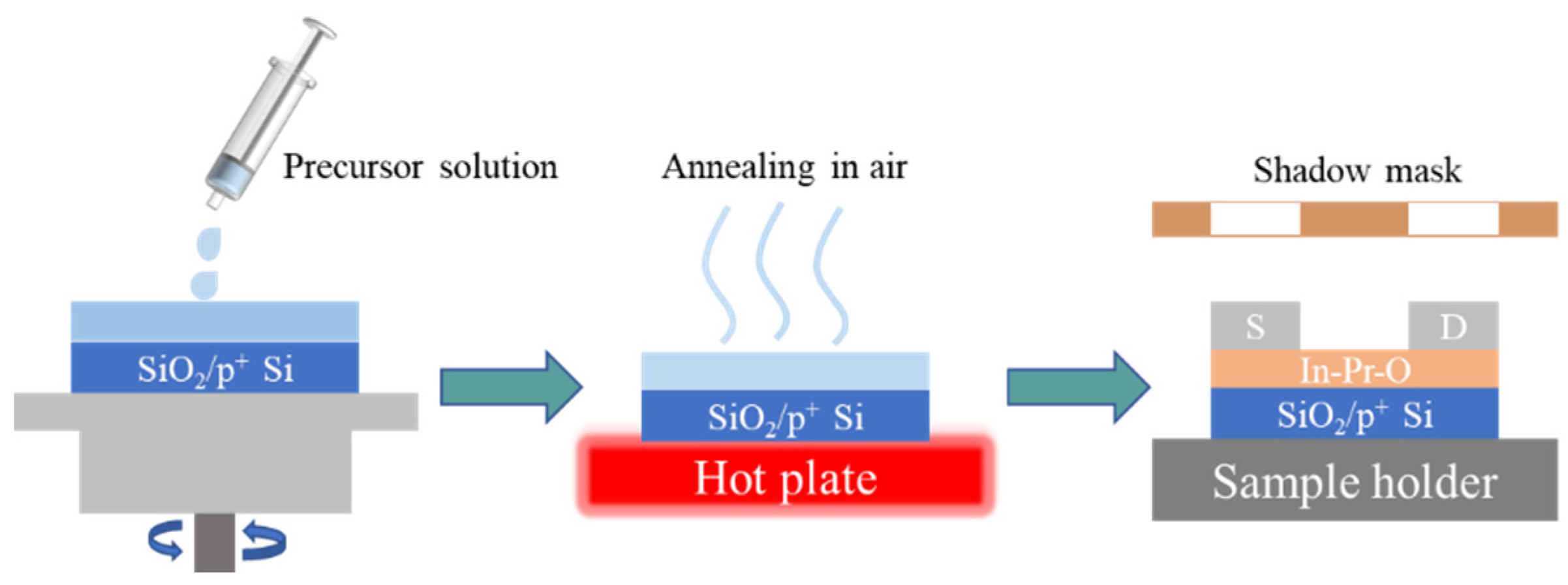
2. Experimental Section

The 0.2 M In-Pr-O precursor solutions for spin-casting were prepared by mixing InN3O9∙xH2O and PrN3O9∙xH2O in DI water with Pr ratios of 0, 2, 5, and 10 mol%. The as-prepared In-Pr-O solutions were stirred rigorously at room temperature and then filtered before spin-casting. The In-Pr-O layers (~6 nm) were deposited by spin coating the precursor solutions on pre-cleaned SiO2 (100 nm)/p+-Si substrates and pre-baked at 150 ℃ and then annealed at 350 ℃ for 1 h. Finally, Al source and drain electrodes (100 nm-thick) were deposited and patterned by shadow masks with a width of 1500 μm and a length of 100 μm to finish manufacturing the In-Pr-O devices. A simple schematic diagram of the In-Pr-O TFTs preparation process is shown in Figure 1.
The crystallinities of the In-Pr-O layers were revealed by grazing incident X-ray diffraction. By using X-ray reflectivity, the thicknesses of the In-Pr-O thin films were verified. The morphologies of the In-Pr-O thin films were observed by Atomic force microscopy. X-ray photoelectron spectroscopy analysis was performed to determine the chemical properties of In-Pr-O thin films. Ultraviolet-visible and photoluminescence spectra of In-Pr-O thin films were also recorded. The typical device performances of In-Pr-O TFTs were measured by a semiconductor parameter in ambient environment at room temperature.

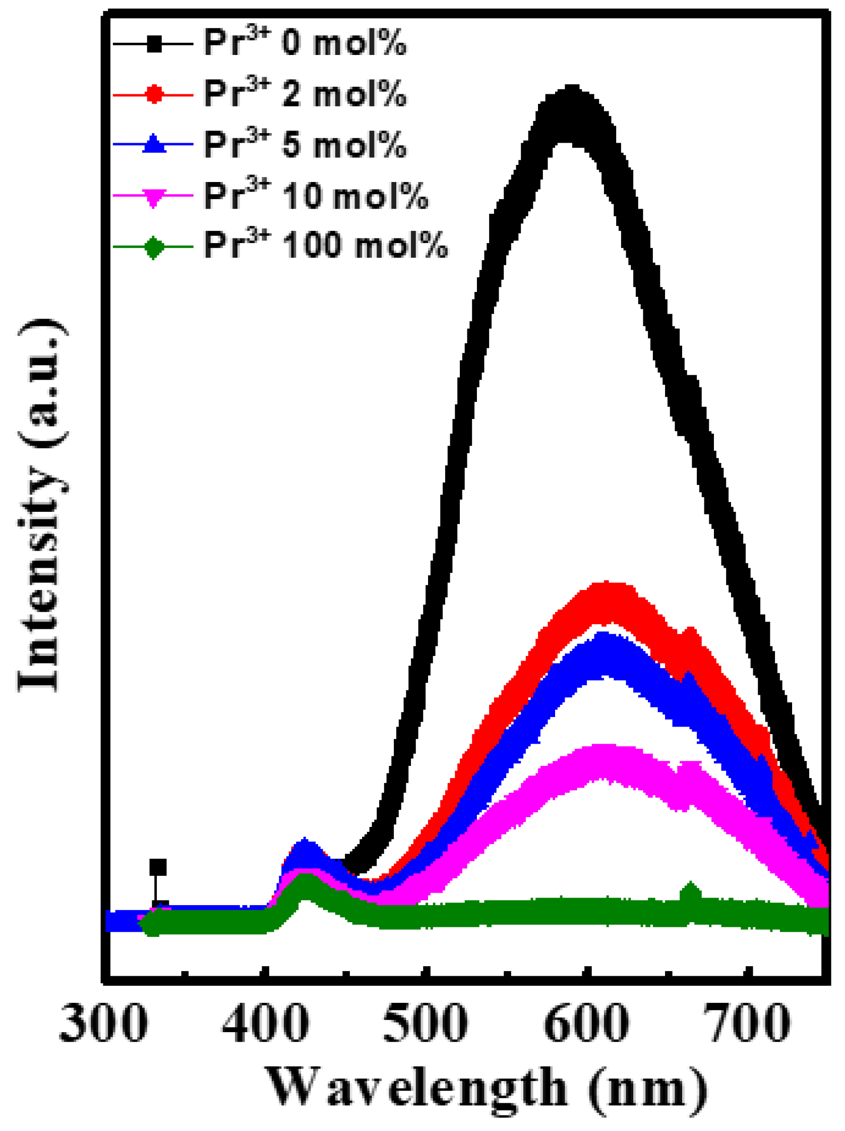
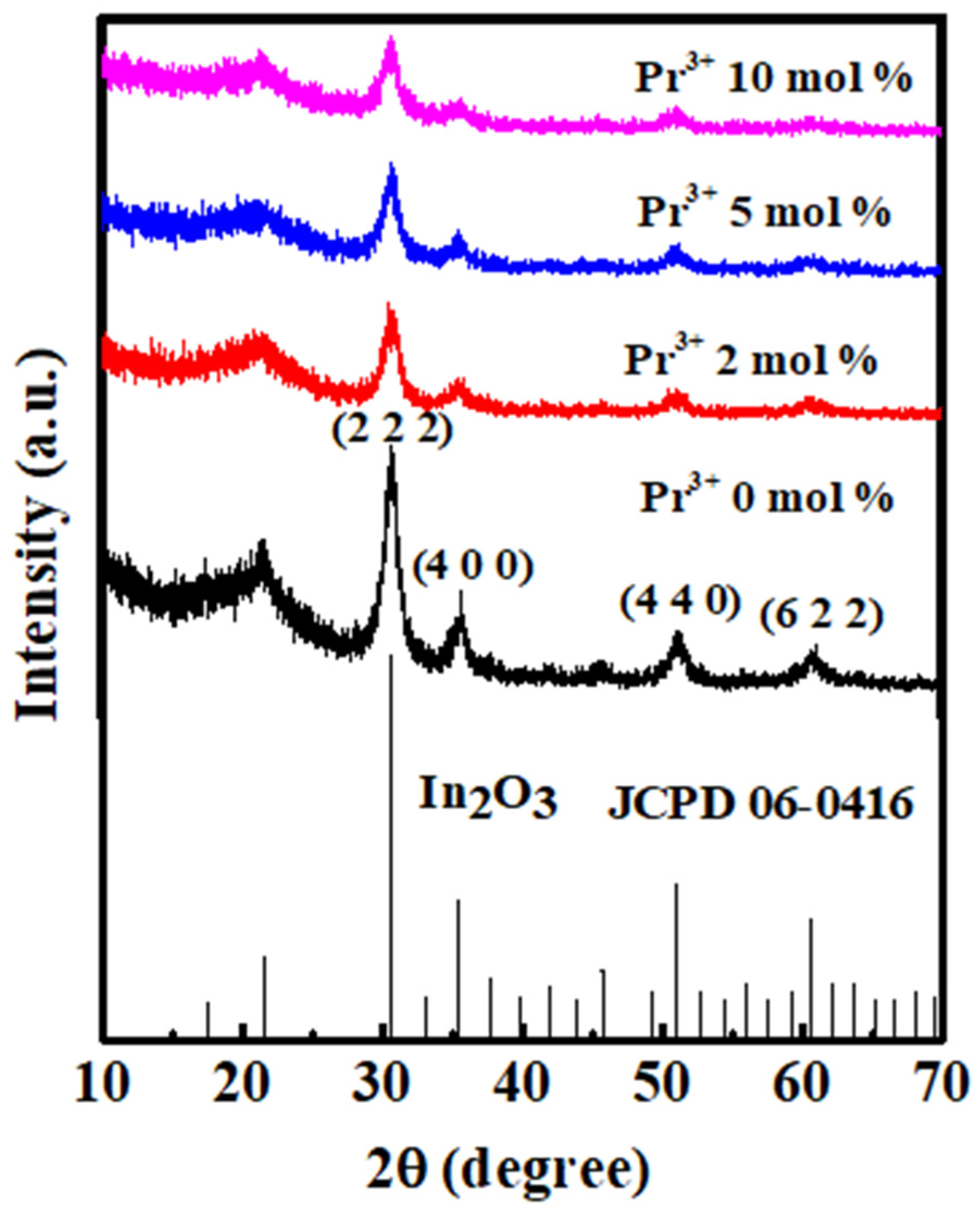
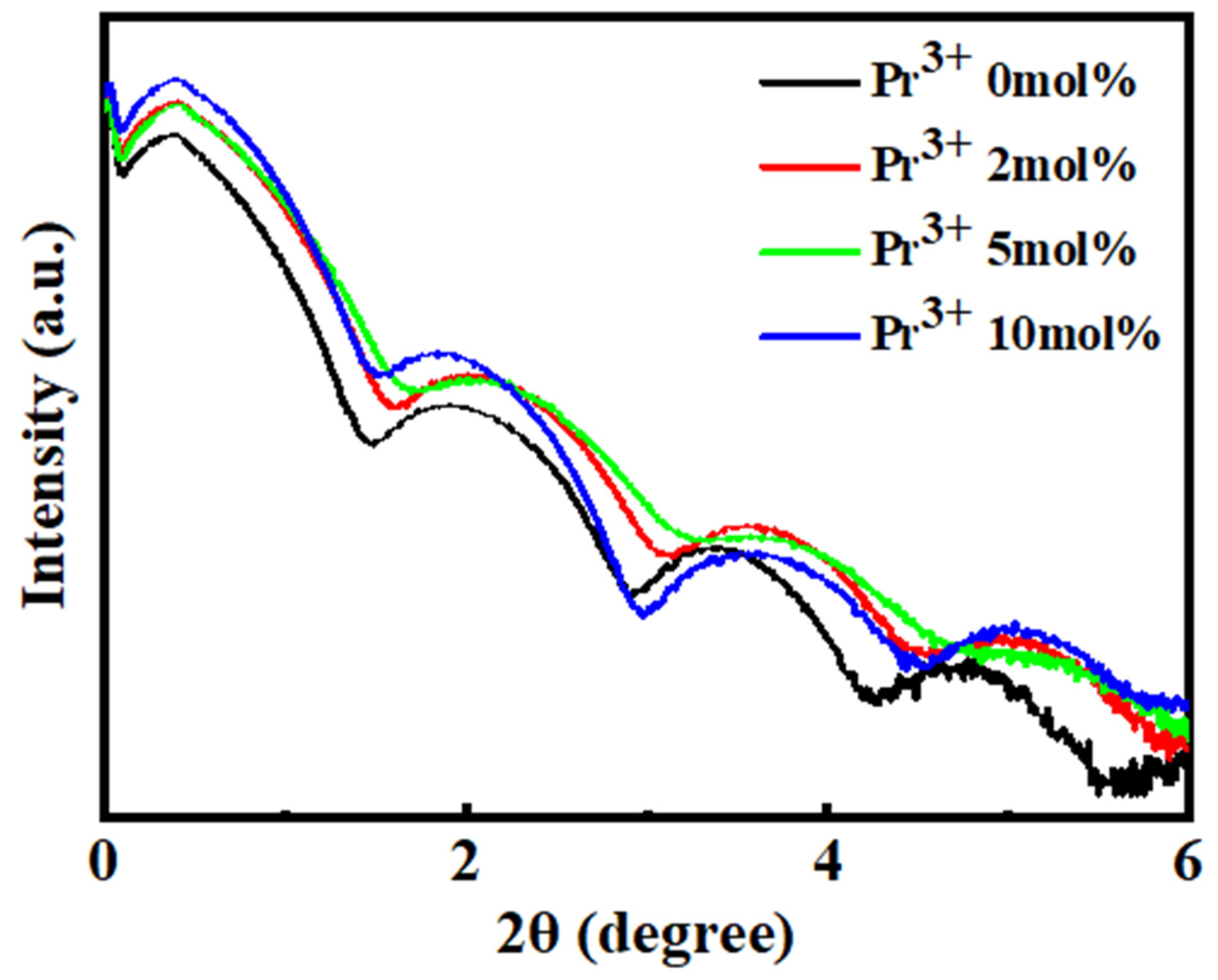
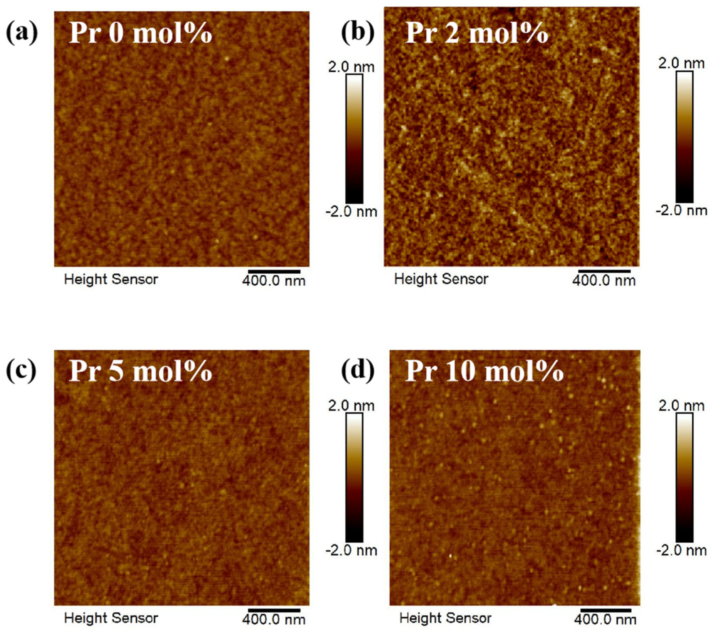
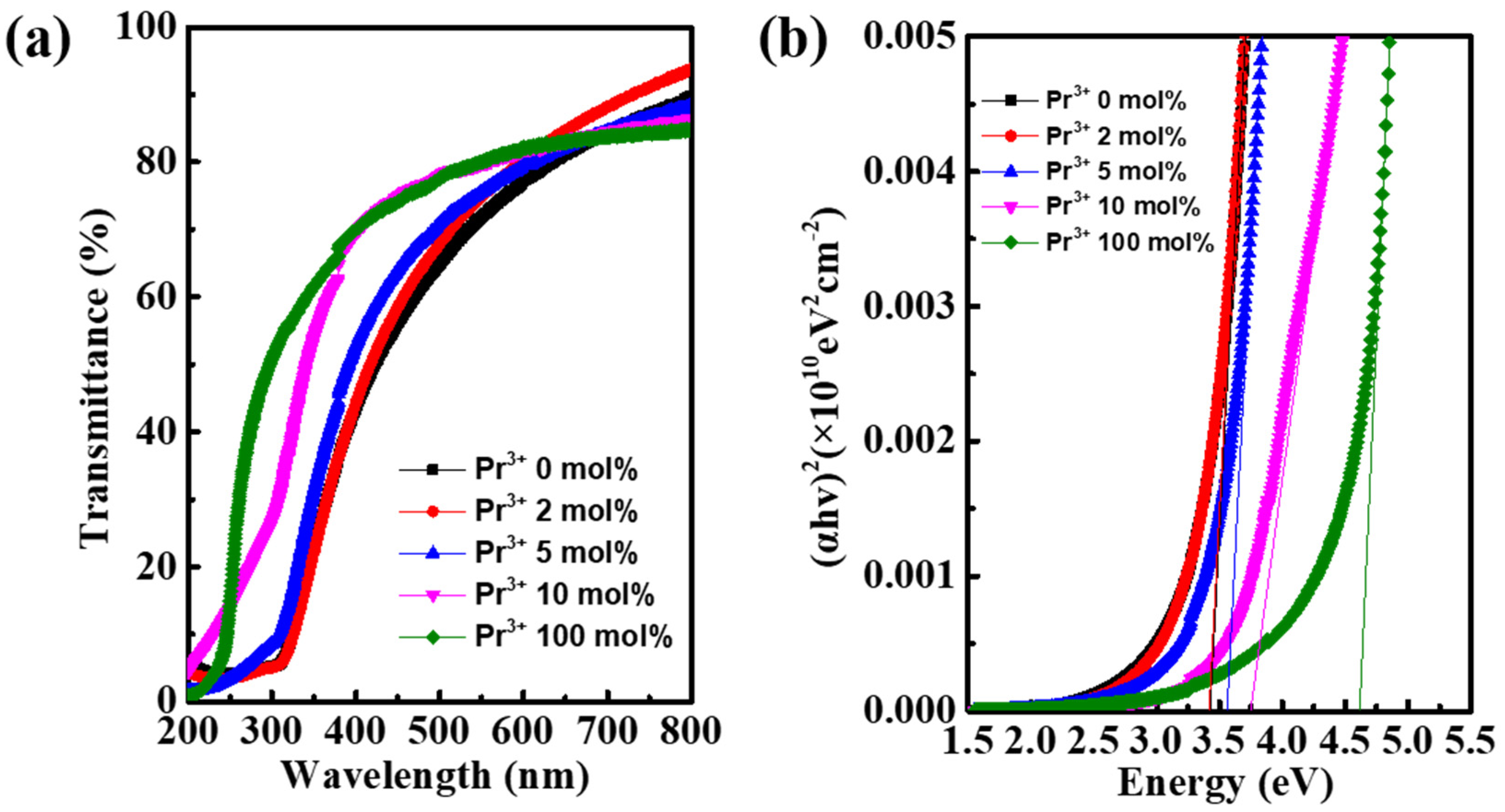
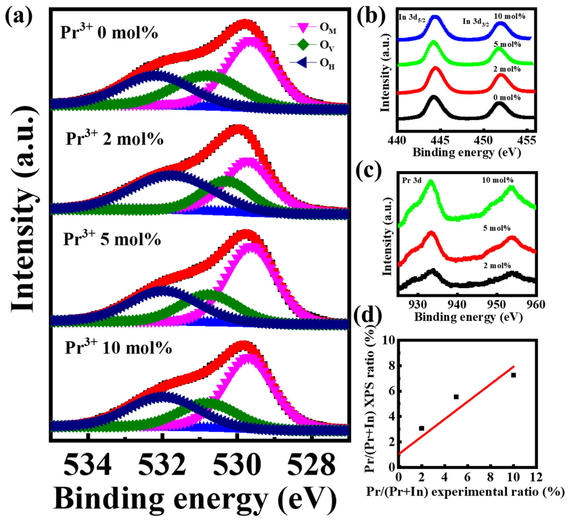
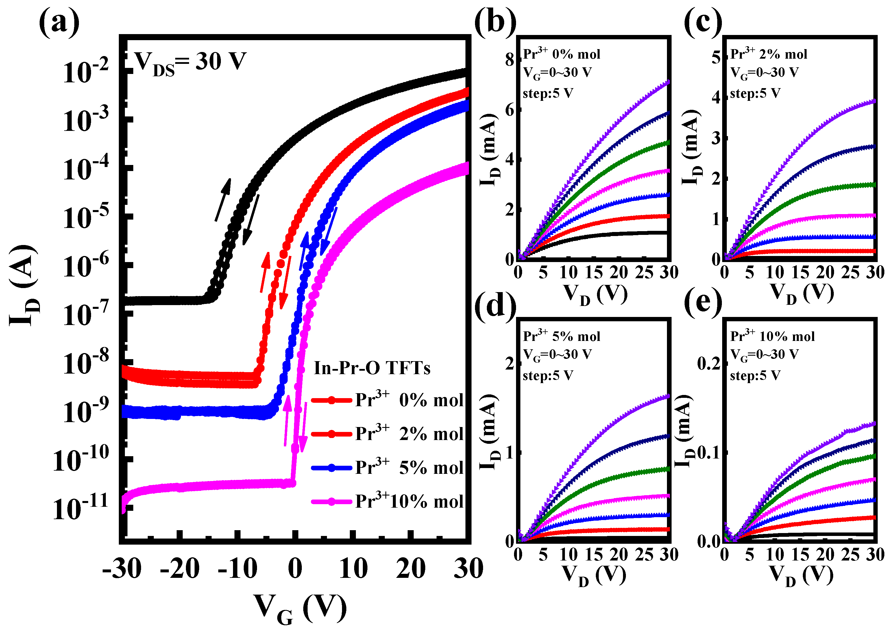
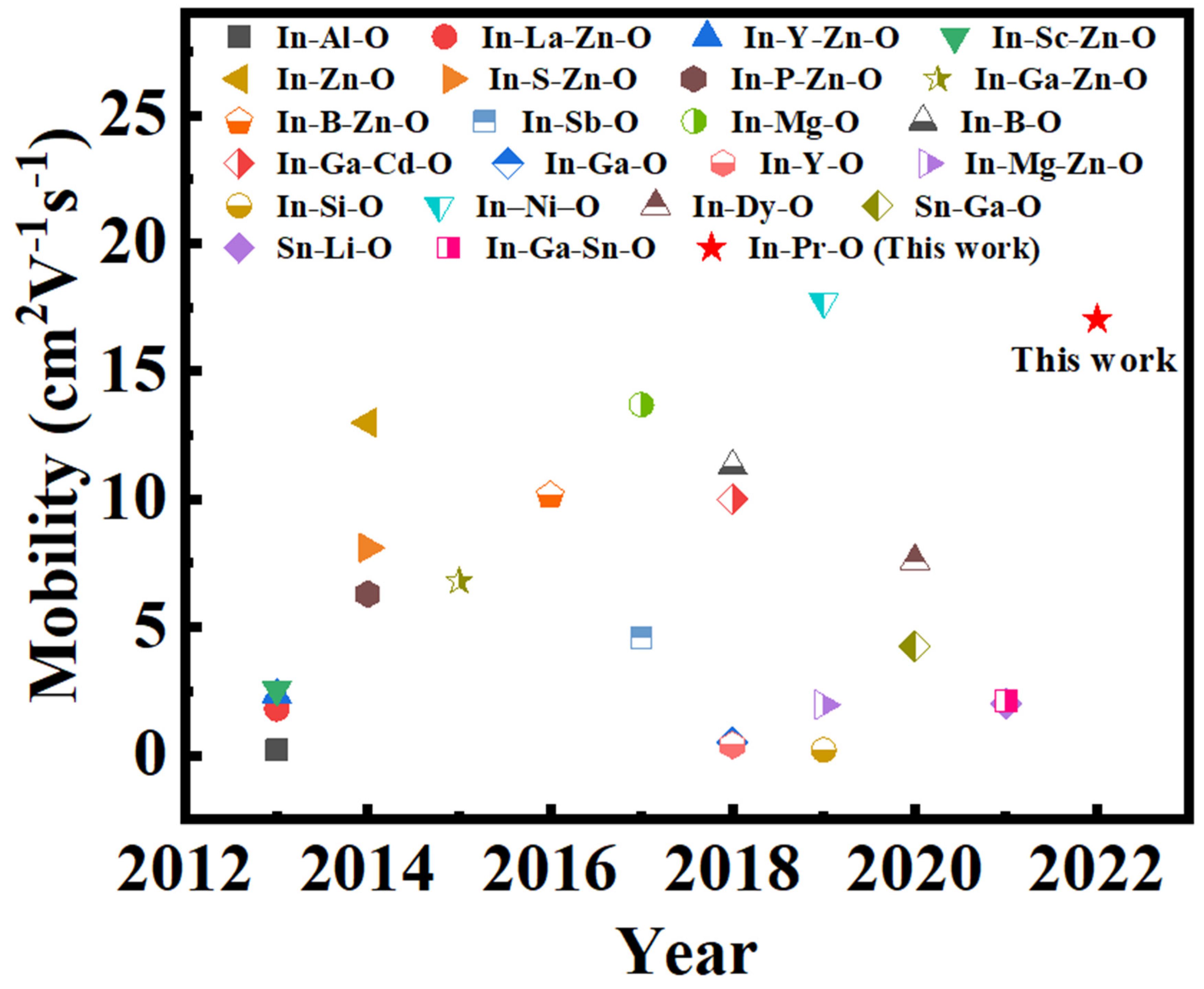
3. Results and Discussion

The grazing incidence X-ray diffraction data of In-Pr-O layers with indicated Pr ratios are displayed in Figure 2. X-ray diffraction analysis reveals that the aqueous solution-processed In-Pr-O films are polycrystalline with (222) the dominant peak as well as weaker (400), (440), and (622) reflections, all belonging to the pristine In2O3 lattice [11]. Therefore, the incorporation of Pr does not break the In2O3 structure. The lattice constants of the In-Pr-O films could be extracted from the prominent peak positions of (222). Hence, the lattice constants of 0, 2, 5, and 10 mol% Pr-doped In2O3 are calculated to be 10.098 ± 0.003, 10.111 ± 0.009, 10.124 ± 0.005, and 10.129 ± 0.002 Å, respectively [10]. Since the Pr3+ has a lager ionic radius (0.1013 Å) than In3+ (0.0800 Å), the substitution of Pr3+ for In3+ will expand the lattice and leads to the increase of the lattice constant. Similar phenomena also appeared in previous research [16,19,20]. Furthermore, the (222) peak intensity becomes weaker after Pr incorporation, suggesting the decrease of crystallinity.
To evaluate the thicknesses of the In-Pr-O thin films, we performed X-ray reflectivity characterization, as shown in Figure 3. The observed thickness of the In-Pr-O films with 0, 2, 5, and 10% Pr contents were 5.74 ± 0.24, 5.78 ± 0.21, 5.83 ± 0.17, and 6.15 ± 0.19 nm, respectively. The thickness of the In-Pr-O film gradually increases with the increase of Pr doping, but it is well maintained at around 6 nm. The slight increase of thickness may be due to the relatively higher viscosity of Pr precursor than that of In.
To access the morphology information, atomic force microscopy was performed. All of the In-Pr-O films exhibit smooth morphologies, as depicted in Figure 4. The In-Pr-O films that were 0, 2, 5, and 10% Pr-doped had a root mean square (RMS) roughness of 0.175 ± 0.036, 0.172 ± 0.029, 0.161 ± 0.034, and 0.202 ± 0.059 nm, respectively. It is an interesting observation that atomically smooth crystalline ternary oxides could be grown from simple aqueous solution. The ultrasmooth semiconductor morphology is indispensable for TFT, since it guarantees low interface trap states as well as good ohmic contacts with the electrodes. Consequently, the near-atomic smoothness of In-Pr-O thin film shows great potential for electronic devices, as will be discussed later.
Figure 5a demonstrates the optical transmittance for In-Pr-O layers with various Pr ratios. All the In-Pr-O films exhibit transmittance higher than 80%, indicating the availability for transparent electronics. Besides, the absorption edge shifts to the shorter wavelength region with the rise of Pr contents. The optical bandgap of In-Pr-O could be deduced using the Tauc formula, as illustrated in Figure 5b. As the Pr ratio increases from 0 to 10 mol%, the optical bandgap shifts from ~3.416 to ~3.747 eV. Additionally, the optical bandgap of pristine Pr2O3 was also measured to be ~4.615 eV. Therefore, the enlarged optical bandgap after Pr doping is due to the lager bandgap of Pr2O3, which would lead to the reduction of electron concentration. Figure 6 shows the photoluminescence spectra of In-Pr-O with different Pr concentrations. According to previous studies, the dominant broad peak centered at around 600 nm is ascribed to oxygen vacancy-related defects [10,18]. Consequently, the decrease of peak intensity after Pr incorporation suggests the reduction of oxygen vacancy-related defects.
X-ray photoelectron spectroscopy was performed to analyze the electronic structure of In-Pr-O thin films. Figure 7a plots the O 1s peaks for In-Pr-O films with indicated Pr doping contents. The O 1s peak could be decomposed into three subpeaks centered at ~529.7 eV for the M-O-M, ~530.7 eV for the oxygen vacancies, and ~532.1 eV for the OH groups. It turns out that the ratio of oxygen vacancies decreases from ~26.16% to ~19.23% as the Pr ratio increases from 0% to 10%. This result supports the PL and UV-visible transmittance analyses’ findings that the addition of Pr could prevent the formation of oxygen vacancies and lower the carrier concentration. The standard electrode potential of Pr (−2.353 V) is lower than In (−0.34 V), the electronegativity of Pr (1.1) is lower than In (1.78), and bond strength of Pr-O (740 kJ/mol) is stronger than that of In-O (320 kJ/mol). Therefore, Pr doping could greatly reduce the oxygen vacancies in pristine In2O3. The In 3d and Pr 3d peaks are plotted in Figure 7b,c, confirming the presence of In-O and Pr-O bonding. As shown in Figure 7d, the Pr doping content in the In-Pr-O thin film is similar to that of the precursor solution.
Figure 8 shows the typical transfer (VD = 30 V) and output curves for Pr doped In2O3 TFTs. We measured at least 10 TFT devices for each Pr doping ratio, and obtained the corresponding statistical deviations, relevant electrical parameters were summarized in Table 1. The undoped In2O3 device has high mobility (μ) of 28.15 ± 1.27 cm2/Vs; however, it encounters high off-state current (Ioff) and large negative threshold voltage (VT). The Ioff decreases from ~10−7 A to ~10−11 A as the Pr ratio rises from 0 mol% to 10 mol%, and the VT shifts from −6.88 ± 0.27 V to 5.77 ± 0.48 V. The improvement of Ioff and VT is due to the reduction of carrier concentration, and originated from the suppression of oxygen vacancy-related defects. Furthermore, the subthreshold slope (S) also improves after Pr doping. Note that S value reflects the channel/dielectric interface trap states. The improved performance of S indicates the lowering of interface trap states also associated with oxygen vacancy-related defects. However, after Pr introduction, the In 5 s orbitals overlap decreases, resulting in the reduction of device mobility. The hysteresis of the In-Pr-O TFTs with 0, 2, 5, and 10% Pr ratios are around 1.32, 0.69, 0.44, 0.15 V, respectively. Note that as the doping amount of Pr increases, the hysteresis of In-Pr-O TFTs gradually weakens. Pr incorporation could suppress the oxygen vacancy-related defects and reduce the channel/dielectric interface trap states, leading to the improvement of hysteresis. The In-Pr-O TFTs with 5 mol% Pr demonstrate the best overall electrical characteristics, including μ of 17.03 ± 1.19 cm2/Vs, Ion/Ioff of ~106, S of 1.32 ± 0.06 V/dec, and VT of 4.86 ± 0.32 V, respectively.
Figure 9 plots the fluctuations in the transfer curves for In-Pr-O TFTs under positive bias stress (PBS, VG = 20 V) for 30 min with 5 min intervals. When subjected to PBS for 30 min, the 0, 2, 5, and 10 mol% Pr-doped In2O3 TFTs show VT shifts of around 13.96, 3.31, 1.86, and 1.43 V, respectively. According to previous research, the positive VT shift under PBS is usually due to several factors [16,18,21]. First, the positive VT shift is attributed to electrons trapping phenomena at the at the In-Pr-O channel or channel/dielectric interface [16,18,21]. The undoped In2O3 has high interface trap states (as reflected by the large subthreshold swing), which is related to the high oxygen vacancy-related defects. Under PBS, these defects can screen applied gate bias by capturing electron carriers from the conduction band, necessitating a greater positive gate bias in order to turn on the devices [21]. This leads to serious positive VT shift under PBS. The Pr incorporation could suppress the oxygen vacancy-related defects and reduce the channel/dielectric interface trap states, leading to the improvement of PBS durability. Secondly, negatively charged species (O2(s)) can be produced by the oxygen species absorbed from the ambient atmosphere capturing electrons in the conducting channel, expressed by O2(g) + e↔O2(s) [22,23], where e denotes electrons, O2(g) and O2(s) represent the neutral and charged oxygen molecules in the back channel. As the electrons concentration increased under PBS, the reaction moved toward the right side of the equation [22,23]. Therefore, the positive VT shift also arises from the consequent accumulation of O2(s) negative charges [18,22,23]. Considering that all the channel layers are extremely thin (~6 nm), the surface adsorption of O2 molecules may also seriously affect the PBS stability. The undoped In2O3 contains a large amount of oxygen-vacancy defects, which tend to absorb more O2 molecules than the Pr-doped samples, causing a larger positive VT shift. Additionally, we note that the shift between 0 and 5 min is large under PBS especially for the pristine In2O3 TFTs, meaning there is a possibility that characteristic degradation has occurred at the beginning of the shift. Therefore, the defect creation may also occur in the undoped In2O3 sample [21]. As shown in Figure 9e, the incorporation of Pr could greatly enhance the PBS stability of the In2O3 devices, in good agreement with the hysteresis characteristics improvement shown in Figure 8 above.
Figure 10 plots the fluctuations in the transfer curves for In-Pr-O devices under negative bias stress (NBS, VG = −20 V) for 30 min with 5 min intervals. When subjected to PBS for 30 min, the 0, 2, 5, and 10 mol% Pr-doped In2O3 TFTs show VT shifts of around −6.14, −5.09, −2.09, −1.39 V, respectively. It is reported that NBS increases the number of holes in the channel layer, causing the adsorbed H2O(g) from the atmosphere to form positively charged H2O+(s) [22,23]. This is described by the following chemical reaction: H2O(g)+h+↔H2O+(s) [22,23], where h+ is a hole. H2O(g) and H2O+(s) represent the neutral and positively charged water molecules in the back channel, respectively. This results in a negative VT shift [18,22,23]. On the other hand, occupied oxygen-vacancy generates deep trap states that are widely distributed above the VBM. Under NBS, a negative gate bias will induce hole trapping at the deep level traps and a larger negative VG is required for turning-on TFTs [21]. This results in the negative shift of VT. Pr incorporation could reduce the level of oxygen-related defects and hence improve the NBS stability [21].
We summarize the recent advances of solution-derived oxide TFTs based on conventional Si/SiO2, as illustrated in Figure 11 and Table S1. Our novel In-Pr-O device presents state-of-the-art mobility. This achievement is due to the low electronegativity and standard electrode potential of Pr, high bond strength of Pr-O, the same bixbyite structure of Pr2O3 and In2O3, as well as the In-Pr-O channel’s atomic smooth nature. It is suggested that reducing the thickness of semiconductors to a few nanometers thick could improve short-channel immunity in scaled devices [10,24]. Therefore, our ultra-thin body In-Pr-O channel also holds great promise for next-generation scaled transistors. Moreover, reducing the thickness is known to substantially increase the flexibility of the material; thus, the In-Pr-O channel with nanoscale thicknesses could withstand high mechanical strain and thus favors flexible electronics [25].

4. Conclusions

We first report the synthesis and characterization of water-induced nanometer-thin (~6 nm) and near atomically smooth (~0.2 nm) crystalline In-Pr-O channel layer. Through various physical and chemical characterizations, the role of Pr doping could be summarized as follows: (1) decrease the crystallinity; (2) enlarge the bandgap of In2O3; (3) suppress the oxygen vacancy-related defects of In2O3. The incorporation of Pr has weakened the mobility of In2O3 TFT s to a certain extent. However, the other electrical parameters including on/off current ratio, subthreshold swing, threshold voltage, hysteresis, and stabilities under PBS and NBS are greatly improved after Pr doping. The optimized In-Pr-O TFT has state-of-the-art electrical performance with mobility of 17.03 ± 1.19 cm2/Vs and on/off current ratio of ~106. The water-induced ultrathin In-Pr-O channel enables future large-scale advanced electronics with green manufacturing.

Supplementary Materials

The following supporting information can be downloaded at: https://www.mdpi.com/article/10.3390/nano12162880/s1, Table S1: Recent advances of solution-processed oxide TFTs based on Si/SiO2 substrate. The references [26,27,28,29,30,31,32,33,34,35,36,37,38,39] are cited in the supplementary materials.

Author Contributions

Conceptualization, W.X.; Formal analysis, W.X.; Funding acquisition, W.X., F.X. and C.Z.; Investigation, W.X., C.X. and Z.Z.; Project administration, W.X.; Supervision, W.X.; Writing—original draft, W.X.; Writing—review & editing, W.X., W.H., Q.L., S.Z., F.X., X.L., D.Z. and C.Z. All authors have read and agreed to the published version of the manuscript.

Funding

This work is supported by the National Natural Science Foundation of China (61704111, 62001308 and 12074263), Shenzhen Science and Technology Program (20200803151643007) and the Pearl River Talents Plan of Guangdong Province (2017GC010092). Fang Xu gratefully acknowledges support from Natural Science Foundation of Top Talent of SZTU (20200219) and Shenzhen Outstanding Scientific and Technological Innovation Talent Training Project (RCBS20210609103736094).

Conflicts of Interest

The authors declare no conflict of interest.

References

  1. Fortunato, E.; Barquinha, P.; Martins, R. Oxide Semiconductor Thin-Film Transistors: A Review of Recent Advances. Adv. Mater. 2012, 24, 2945–2986. [Google Scholar] [CrossRef] [PubMed]
  2. Xu, W.; Li, H.; Xu, J.-B.; Wang, L. Recent Advances of Solution-Processed Metal Oxide Thin-Film Transistors. ACS Appl. Mater. Interfaces 2018, 10, 25878–25901. [Google Scholar] [CrossRef] [PubMed]
  3. Chen, R.; Lan, L. Solution-processed metal-oxide thin-film transistors: A review of recent developments. Nanotechnology 2019, 30, 312001. [Google Scholar] [CrossRef]
  4. Zhu, L.; He, G.; Li, W.; Yang, B.; Fortunato, E.; Martins, R. Nontoxic, Eco-friendly Fully Water-Induced Ternary Zr-Gd-O Dielectric for High-Performance Transistors and Unipolar Inverters. Adv. Electron. Mater. 2018, 4, 1800100. [Google Scholar] [CrossRef]
  5. Yu, X.; Marks, T.J.; Facchetti, A. Metal oxides for optoelectronic applications. Nat. Mater. 2016, 15, 383–396. [Google Scholar] [CrossRef]
  6. Xu, W.; Wang, H.; Xie, F.; Chen, J.; Cao, H.; Xu, J.-B. Facile and Environmentally Friendly Solution-Processed Aluminum Oxide Dielectric for Low-Temperature, High-Performance Oxide Thin-Film Transistors. ACS Appl. Mater. Interfaces 2015, 7, 5803–5810. [Google Scholar] [CrossRef]
  7. Thomas, S.R.; Pattanasattayavong, P.; Anthopoulos, T.D. Solution-processable metal oxide semiconductors for thin-film transistor applications. Chem. Soc. Rev. 2013, 42, 6910–6923. [Google Scholar] [CrossRef]
  8. Kamiya, T.; Hosono, H. Material characteristics and applications of transparent amorphous oxide semiconductors. NPG Asia Mater. 2010, 2, 15–22. [Google Scholar] [CrossRef] [Green Version]
  9. Park, S.; Kim, C.H.; Lee, W.J.; Sung, S.; Yoon, M.-H. Sol-gel metal oxide dielectrics for all-solution-processed electronics. Mater. Sci. Eng. R Rep. 2017, 114, 1–22. [Google Scholar] [CrossRef]
  10. Li, S.; Tian, M.; Gao, Q.; Wang, M.; Li, T.; Hu, Q.; Li, X.; Wu, Y. Nanometre-thin indium tin oxide for advanced high-performance electronics. Nat. Mater. 2019, 18, 1091–1097. [Google Scholar] [CrossRef]
  11. Zhang, X.; Wang, B.; Huang, W.; Chen, Y.; Wang, G.; Zeng, L.; Zhu, W.; Bedzyk, M.J.; Zhang, W.; Medvedeva, J.E.; et al. Synergistic Boron Doping of Semiconductor and Dielectric Layers for High-Performance Metal Oxide Transistors: Interplay of Experiment and Theory. J. Am. Chem. Soc. 2018, 140, 12501–12510. [Google Scholar] [CrossRef] [PubMed]
  12. Kirmani, A.R.; Chen, H.; Stafford, C.M.; Bittle, E.G.; Richter, L.J. Coating Thickness Controls Crystallinity and Enables Homoepitaxial Growth of Ultra-Thin-Channel Blade-Coated In2O3 Transistors. Adv. Electron. Mater. 2020, 6, 2000354. [Google Scholar] [CrossRef]
  13. Liu, G.; Liu, A.; Zhu, H.; Shin, B.; Fortunato, E.; Martins, R.; Wang, Y.; Shan, F. Low-Temperature, Nontoxic Water-Induced Metal-Oxide Thin Films and Their Application in Thin-Film Transistors. Adv. Funct. Mater. 2015, 25, 2564–2572. [Google Scholar] [CrossRef]
  14. Hwang, Y.H.; Seo, J.-S.; Yun, J.M.; Park, H.; Yang, S.; Park, S.-H.K.; Bae, B.-S. An ‘aqueous route’ for the fabrication of low-temperature-processable oxide flexible transparent thin-film transistors on plastic substrates. NPG Asia Mater. 2013, 5, e45. [Google Scholar] [CrossRef] [Green Version]
  15. Parthiban, S.; Kwon, J.-Y. Role of dopants as a carrier suppressor and strong oxygen binder in amorphous indium-oxide-based field effect transistor. J. Mater. Res. 2014, 29, 1585–1596. [Google Scholar] [CrossRef] [Green Version]
  16. Li, Y.; Zhu, D.; Xu, W.; Han, S.; Fang, M.; Liu, W.; Cao, P.; Lu, Y. High-mobility nanometer-thick crystalline In–Sm–O thin-film transistors via aqueous solution processing. J. Mater. Chem. C 2020, 8, 310–318. [Google Scholar] [CrossRef]
  17. Lin, Z.; Lan, L.; Sun, S.; Li, Y.; Song, W.; Gao, P.; Song, E.; Zhang, P.; Li, M.; Wang, L.; et al. Solution-processed high-mobility neodymium-substituted indium oxide thin-film transistors formed by facile patterning based on aqueous precursors. Appl. Phys. Lett. 2017, 110, 133502. [Google Scholar] [CrossRef]
  18. Li, Y.; Xu, W.; Liu, W.; Han, S.; Cao, P.; Fang, M.; Zhu, D.; Lu, Y. High-Performance Thin-Film Transistors with Aqueous Solution-Processed NiInO Channel Layer. ACS Appl. Electron. Mater. 2019, 1, 1842–1851. [Google Scholar] [CrossRef]
  19. Lee, S.-H.; Kim, T.; Lee, J.; Avis, C.; Jang, J. Solution-processed gadolinium doped indium-oxide thin-film transistors with oxide passivation. Appl. Phys. Lett. 2017, 110, 122102. [Google Scholar] [CrossRef]
  20. Kim, J.-S.; Na, C.; Kwak, C.-H.; Li, H.-Y.; Yoon, J.; Kim, J.-H.; Jeong, S.-Y.; Lee, J.-H. Humidity-Independent Gas Sensors Using Pr-Doped In2O3 Macroporous Spheres: Role of Cyclic Pr3+/Pr4+ Redox Reactions in Suppression of Water-Poisoning Effect. ACS Appl. Mater. Interfaces 2019, 11, 25322–25329. [Google Scholar] [CrossRef]
  21. Park, H.; Nam, Y.; Jin, J.; Bae, B.-S. Improvement of bias stability of oxyanion-incorporated aqueous sol–gel processed indium zinc oxide TFTs. J. Mater. Chem. C 2014, 2, 5998–6003. [Google Scholar] [CrossRef]
  22. Jeong, J.K.; Yang, H.W.; Jeong, J.H.; Mo, Y.-G.; Kim, H.D. Origin of threshold voltage instability in indium-gallium-zinc oxide thin film transistors. Appl. Phys. Lett. 2008, 93, 123508. [Google Scholar] [CrossRef]
  23. Liu, P.-T.; Chou, Y.-T.; Teng, L.-F. Environment-dependent metastability of passivation-free indium zinc oxide thin film transistor after gate bias stress. Appl. Phys. Lett. 2009, 95, 233504. [Google Scholar] [CrossRef] [Green Version]
  24. Si, M.; Lin, Z.; Chen, Z.; Sun, X.; Wang, H.; Ye, P.D. Scaled indium oxide transistors fabricated using atomic layer deposition. Nat. Electron. 2022, 5, 164–170. [Google Scholar] [CrossRef]
  25. Datta, R.S.; Syed, N.; Zavabeti, A.; Jannat, A.; Mohiuddin, M.; Rokunuzzaman, M.; Zhang, B.Y.; Rahman, A.; Atkin, P.; Messalea, K.A.; et al. Flexible two-dimensional indium tin oxide fabricated using a liquid metal printing technique. Nat. Electron. 2020, 3, 51–58. [Google Scholar] [CrossRef]
  26. Hwang, Y.H.; Bae, B.S. Effect of Aluminum and Gallium Doping on the Performance of Solution-Processed Indium Oxide Thin-Film Transistors. J. Disp. Technol. 2013, 9, 704–709. [Google Scholar] [CrossRef]
  27. Hennek, J.W.; Jeremy, S.; Aiming, Y.; Myung-Gil, K.; Wei, Z.; Dravid, V.P.; Antonio, F.; Marks, T.J. Oxygen “getter” effects on microstructure and carrier transport in low temperature combustion-processed a-InXZnO (X = Ga, Sc, Y, La) transistors. J. Am. Chem. Soc. 2013, 135, 10729–10741. [Google Scholar] [CrossRef]
  28. Yu, X.; Smith, J.; Zhou, N.; Zeng, L.; Guo, P.; Xia, Y.; Alvarez, A.; Aghion, S.; Lin, H.; Yu, J.; et al. Spray-combustion synthesis: Efficient solution route to high-performance oxide transistors. Proc. Natl. Acad. Sci. USA 2015, 112, 3217–3222. [Google Scholar] [CrossRef] [Green Version]
  29. Zhong, D.Y.; Li, J.; Zhao, C.Y.; Huang, C.X.; Zhang, J.H.; Li, X.F.; Jiang, X.Y.; Zhang, Z.L. Enhanced Electrical Performance and Negative Bias Illumination Stability of Solution-Processed InZnO Thin-Film Transistor by Boron Addition. IEEE Trans. Electron Devices 2018, 65, 520–525. [Google Scholar] [CrossRef]
  30. Kim, T.; Jang, B.; Bae, J.H.; Park, H.; Cho, C.S.; Kwon, H.J.; Jang, J. Improvement in the Performance of Sol–Gel Processed In2O3 Thin-Film Transistor Depending on Sb Dopant Concentration. IEEE Electron Device Lett. 2017, 38, 1027. [Google Scholar] [CrossRef]
  31. Zhao, C.Y.; Li, J.; Zhong, D.Y.; Huang, C.X.; Zhang, J.H.; Li, X.F.; Jiang, X.Y.; Zhang, Z.L. Mg Doping to Simultaneously Improve the Electrical Performance and Stability of MgInO Thin-Film Transistors. IEEE Trans. Electron Devices 2017, 64, 2216. [Google Scholar] [CrossRef]
  32. Song, A.; Javaid, K.; Yu, L.; Wu, W.; Yu, J.; Liang, L.; Zhang, H.; Lan, L.; Chang, T.C.; Cao, H. Design, Properties, and TFT Application of Solution-Processed In-Ga-Cd-O Thin Films. Phys. Status Solidi (RRL)—Rapid Res. Lett. 2018, 12, 1800034. [Google Scholar] [CrossRef]
  33. Jaehnike, F.; Pham, D.V.; Bock, C.; Kunze, U. Role of gallium and yttrium dopants on the stability and performance of solution processed indium oxide thin-film transistors. J. Mater. Chem. C 2019, 7, 7627–7635. [Google Scholar] [CrossRef]
  34. Cheng, J.; Li, X.Y.; Guo, J.; Xu, H.F.; Chen, Y.H.; He, Y.F.; Xue, J.S.; Zhang, T.; Yu, Z.N. The role of the sequence of plasma treatment and high temperature annealing on solution-processed a-IMZO thin film transistor. J. Alloys Compd. 2019, 793, 369–374. [Google Scholar] [CrossRef]
  35. Hoang, H.; Hori, T.; Yasuda, T.-o.; Kizu, T.; Tsukagoshi, K.; Nabatame, T.; Trinh, B.; Fujiwara, A. Erratum: Si-doping effect on solution-processed In-O thin-film transistors (2019 Mater. Res. Express 6 026410). Mater. Res. Express 2019, 6, 039601. [Google Scholar] [CrossRef]
  36. Hong, L.; Xu, W.; Liu, W.; Han, S.; Cao, P.; Fang, M.; Zhu, D.; Lu, Y. High performance indium dysprosium oxide thin-film transistors grown from aqueous solution. Appl. Surf. Sci. 2020, 504, 144499. [Google Scholar] [CrossRef]
  37. Zhang, L.; Zhu, D.; Han, S.; Lu, Y.; Fang, M.; Liu, W.; Cao, P.; Xu, W. Aqueous solution deposition of amorphous gallium tin oxide for thin-film transistors applications. Ceram. Int. 2020, 46, 19557–19563. [Google Scholar] [CrossRef]
  38. Kim, H.-J.; Kim, D.-W.; Lee, W.-Y.; Lee, S.-H.; Bae, J.-H.; Kang, I.-M.; Jang, J. Improved Negative Bias Stress Stability of Sol–Gel-Processed Li-Doped SnO2 Thin-Film Transistors. Electronics 2021, 10, 1629. [Google Scholar] [CrossRef]
  39. Kim, H.; Maeng, S.; Lee, S.; Kim, J. Improved Performance and Operational Stability of Solution-Processed InGaSnO (IGTO) Thin Film Transistors by the Formation of Sn–O Complexes. ACS Appl. Electron. Mater. 2021, 3, 1199–1210. [Google Scholar] [CrossRef]
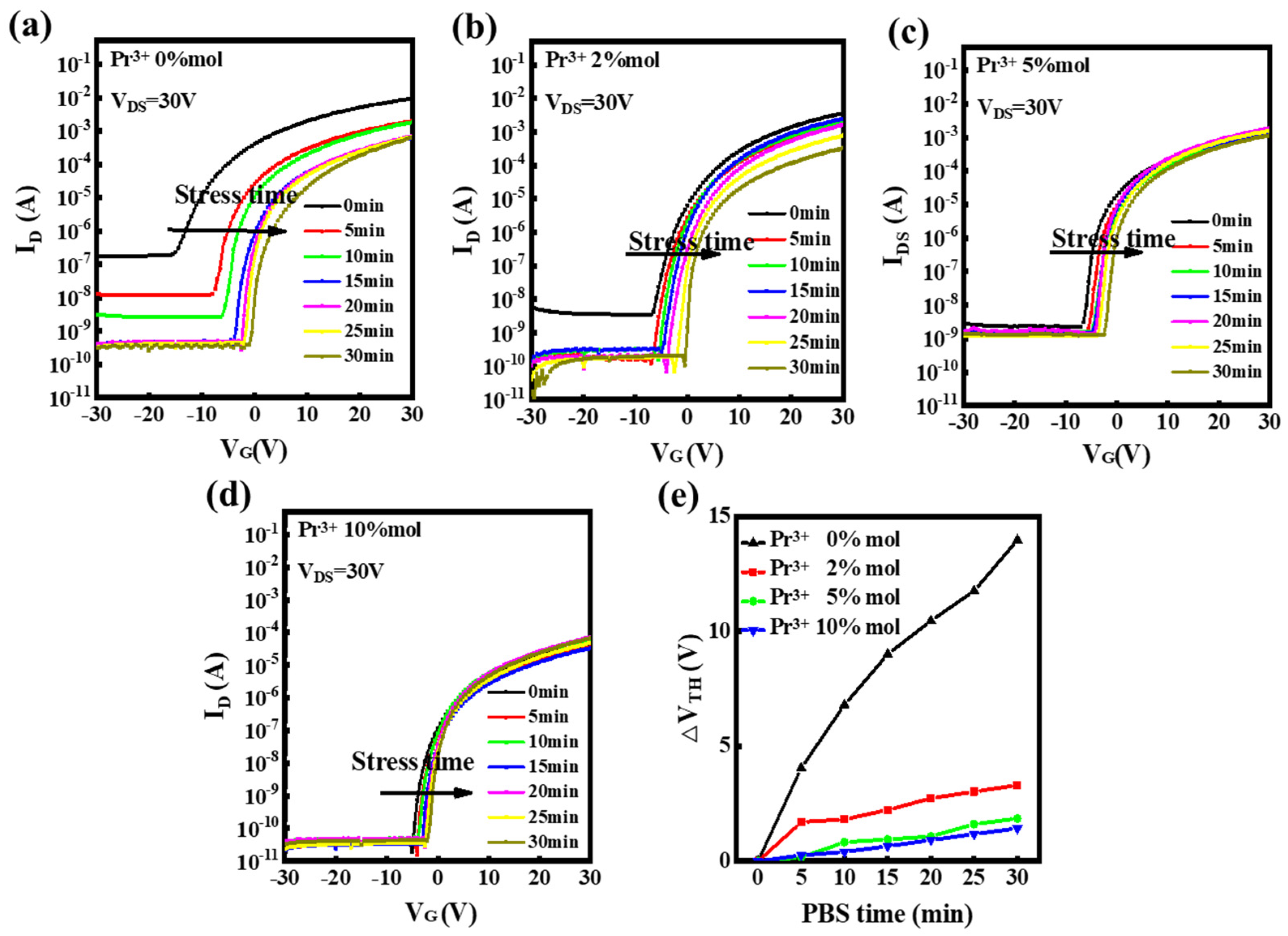
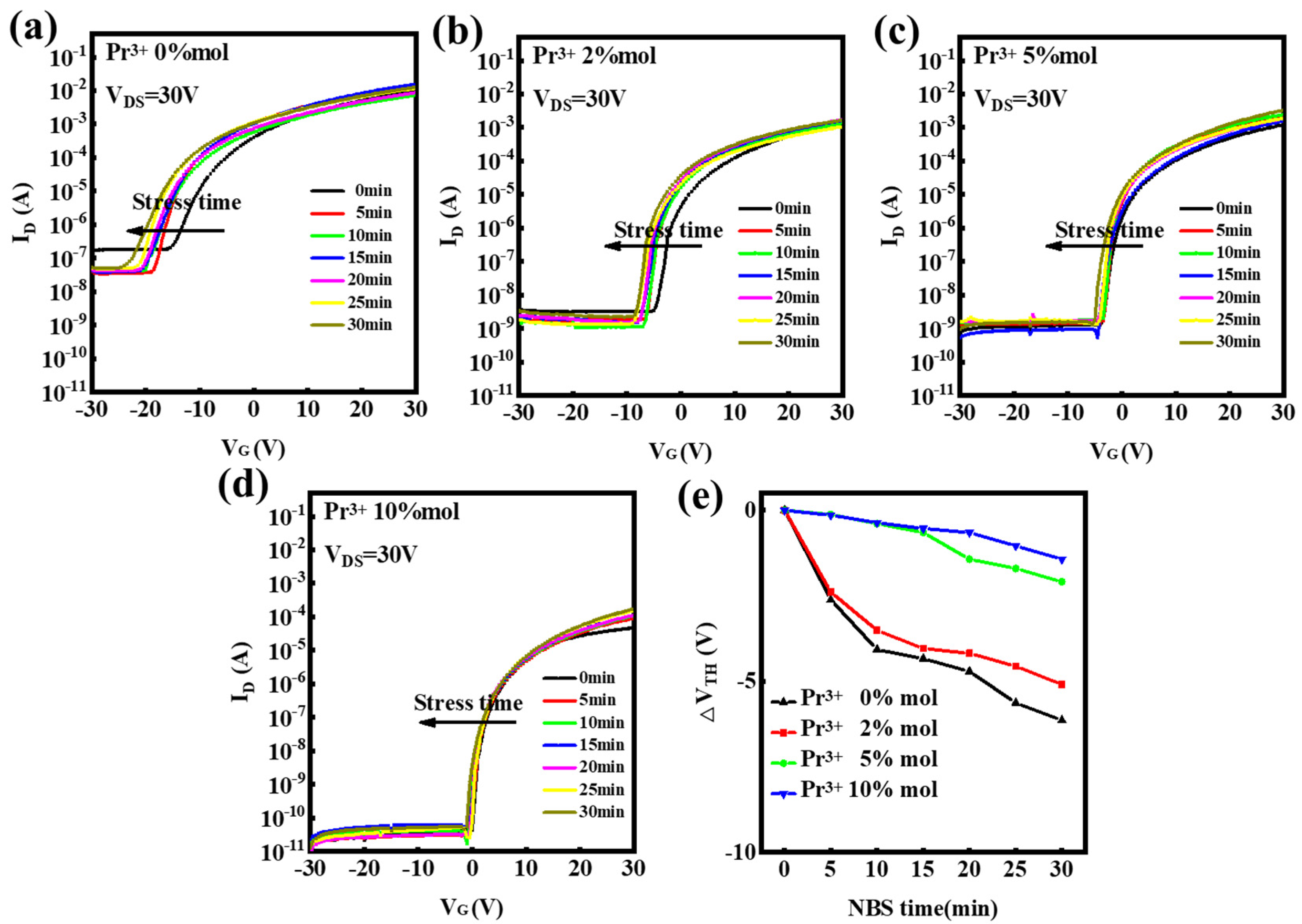
Figure 1. Schematic showing the fabricated In-Pr-O TFTs.
Nanomaterials 12 02880 g001
Figure 2. Grazing incidence X-ray diffraction patterns for In-Pr-O layers with 0, 2, 5, and 10 mol% Pr concentration.
Nanomaterials 12 02880 g002
Figure 3. X-ray reflectivity patterns of In-Pr-O films with various Pr contents.
Nanomaterials 12 02880 g003
Figure 4. Images of In-Pr-O films with with Pr ratios of (a) 0, (b) 2, (c) 5, and (d) 10 mol% by atomic force microscopy.
Nanomaterials 12 02880 g004
Figure 5. (a) Transmittance spectra and (b) evaluation of optical bandgap for In-Pr-O layer with different Pr ratios.
Nanomaterials 12 02880 g005
Figure 6. Photoluminescence spectra for In-Pr-O with indicated Pr concentrations.
Nanomaterials 12 02880 g006
Figure 7. X-ray photoelectron spectroscopy spectra for In-Pr-O films with indicated Pr concentrations. (a) O 1s, (b) In 3d, (c) Pr 3d, and (d) Pr doping ratio between solution and thin film.
Nanomaterials 12 02880 g007
Figure 8. (a) Transfer and (be) output curves for In-Pr-O TFTs with 0, 2, 5, and 10 mol% Pr concentrations.
Nanomaterials 12 02880 g008
Figure 9. Transfer curves variations under positive bias stress for In-Pr-O TFTs with Pr mol% ratios of (a) 0 mol%, (b) 2 mol%, (c) 5 mol%, (d) 10 mol%, and (e) summary of VT shifts.
Nanomaterials 12 02880 g009
Figure 10. Transfer curves variations under negative bias stress for In-Pr-O TFTs with Pr mol% ratios of (a) 0 %, (b) 2 %, (c) 5 %, (d) 10 %, and (e) summary of VT shifts.
Nanomaterials 12 02880 g010
Figure 11. Recent advances of sol–gel oxide TFTs on Si/SiO2 substrate.
Nanomaterials 12 02880 g011
Table 1. Electrical characteristics of In-Pr-O TFTs.
Pr Ratio (%)μ
(cm2V−1s−1)
Ion/IoffS
(V/dec)
VT
(V)
Hysteresis
(V)
VT Shift under PBS
for 30 min (V)
VT Shift under NBS
for 30 min (V)
028.15 ± 1.275.30 × 1042.50 ± 0.13−6.88 ± 0.271.3213.96−6.14
221.87 ± 1.457.05 × 1051.46 ± 0.092.37 ± 0.410.963.31−5.09
517.03 ± 1.192.15×1061.32 ± 0.064.86 ± 0.320.441.86−2.09
100.76 ± 0.141.26 × 1070.51 ± 0.115.77 ± 0.480.151.43−1.39
Publisher’s Note: MDPI stays neutral with regard to jurisdictional claims in published maps and institutional affiliations.

