
Geometric Optimization of Perovskite Solar Cells with Metal Oxide Charge Transport Layers

 ,
,  ,
,  ,
, 
Abstract
:1. Introduction
2. Materials and Methods
2.1. Simulation
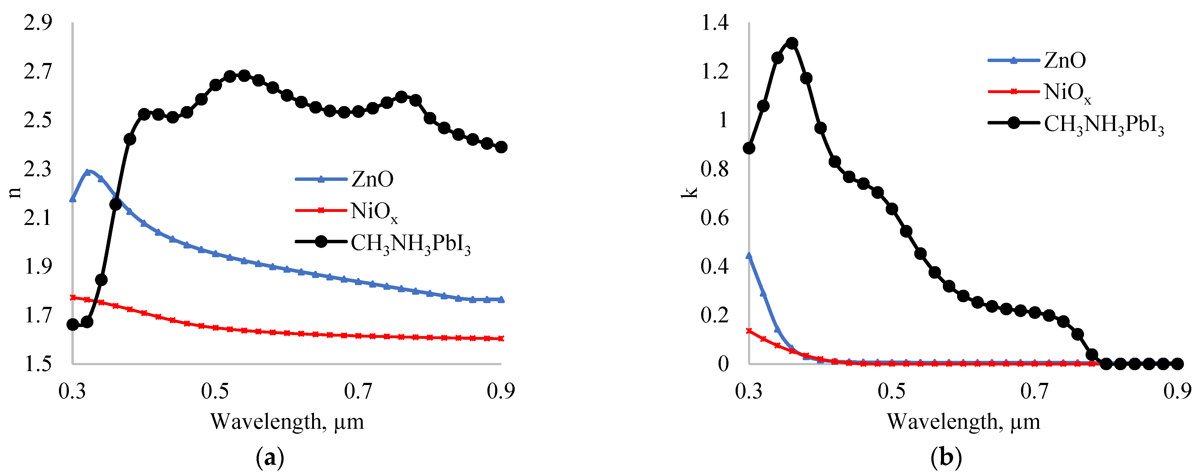
2.2. Physical Parameters of Materials
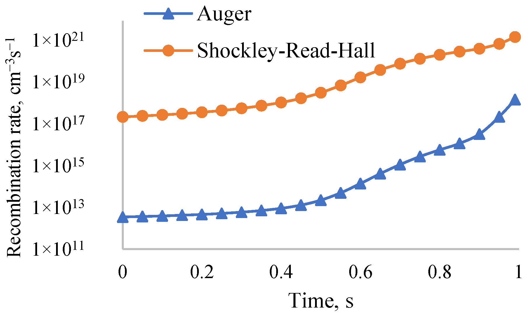
2.3. Physical Background of Simulation
3. Results and Discussion
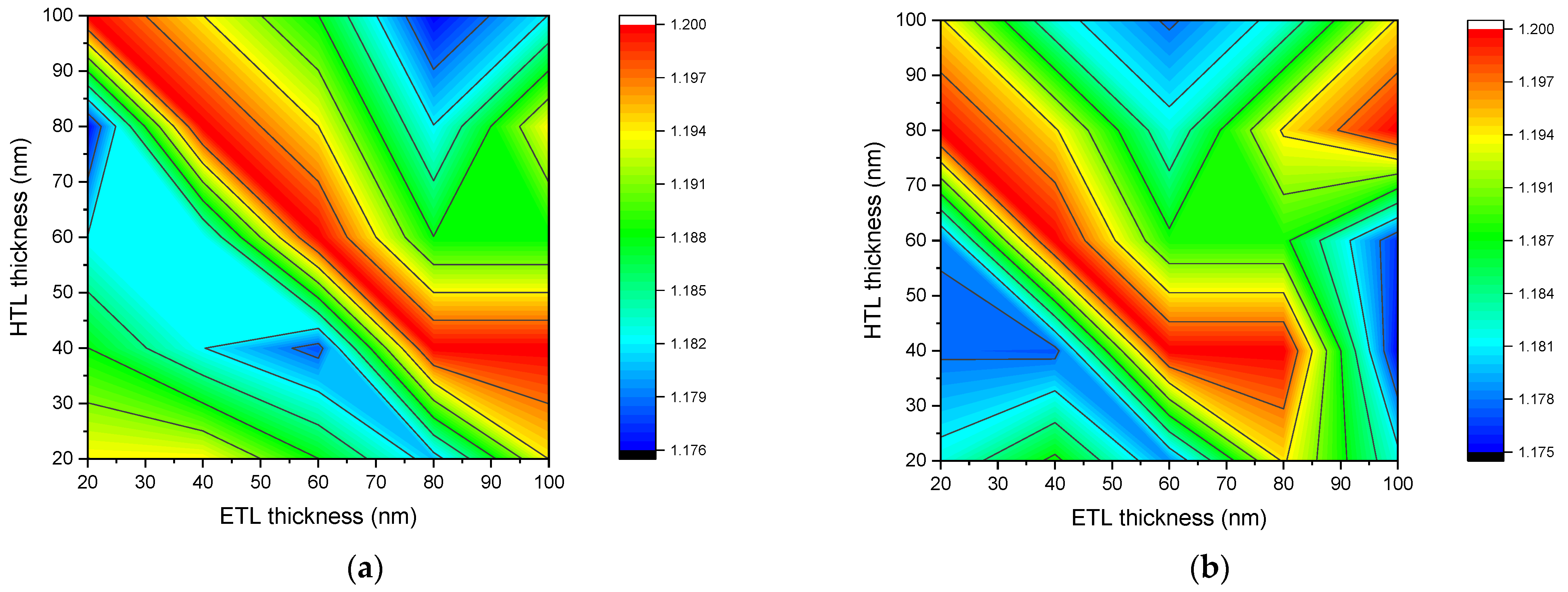
3.1. Open-Circuit Voltage
3.2. Short-Circuit Current
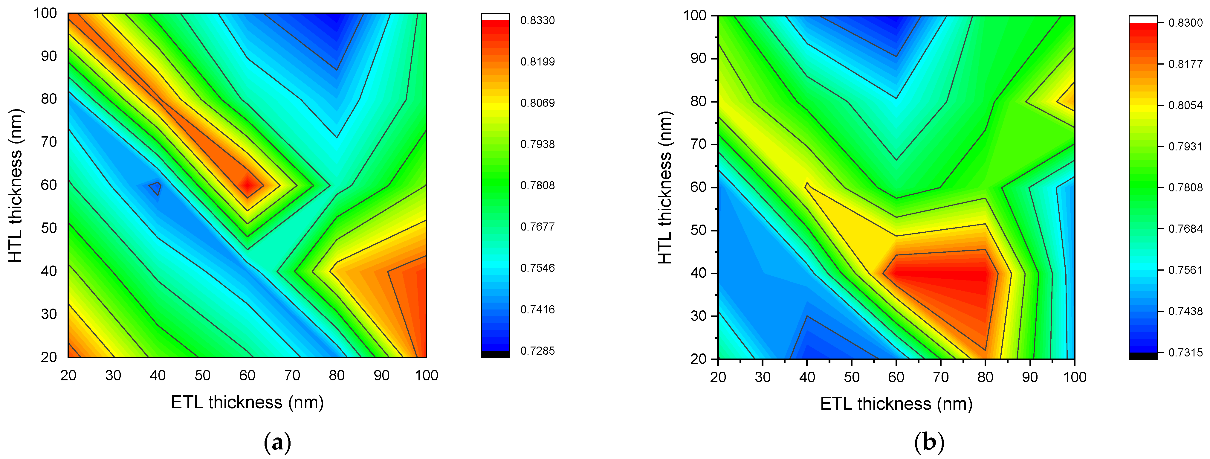
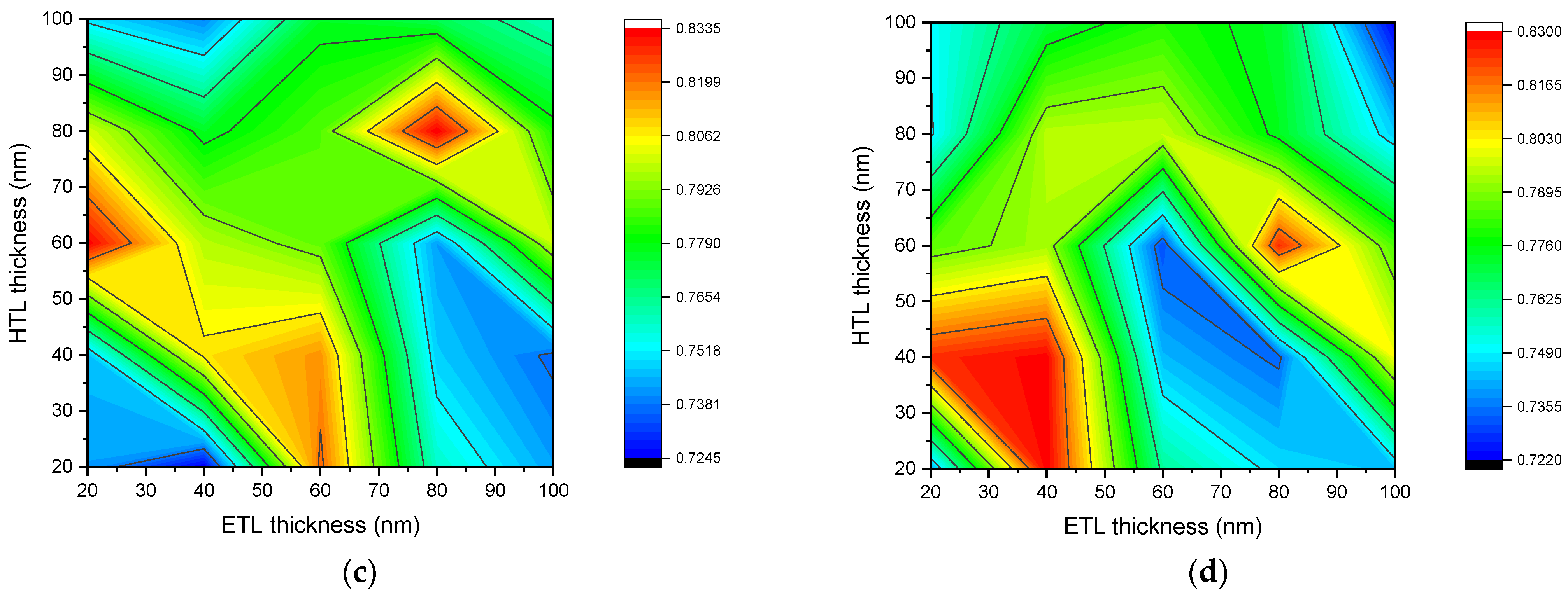
3.3. Fill Factor
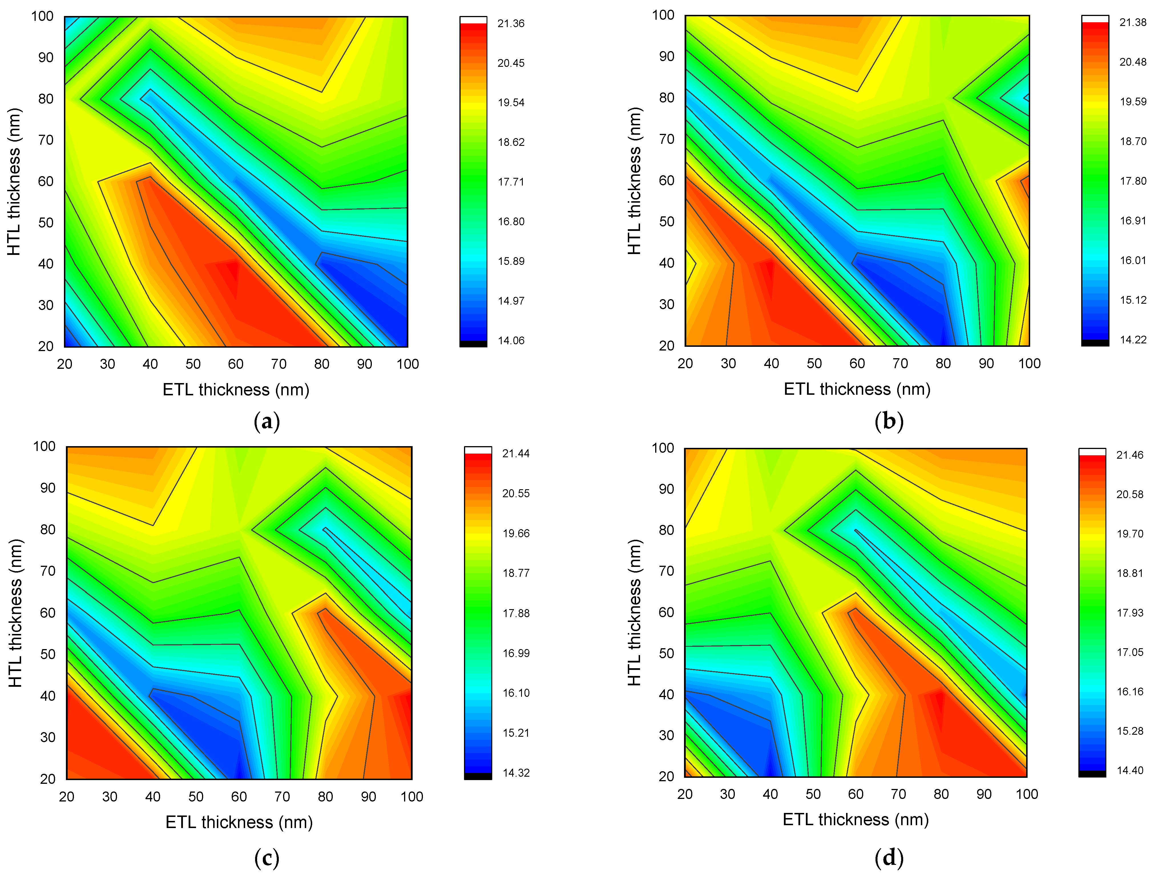
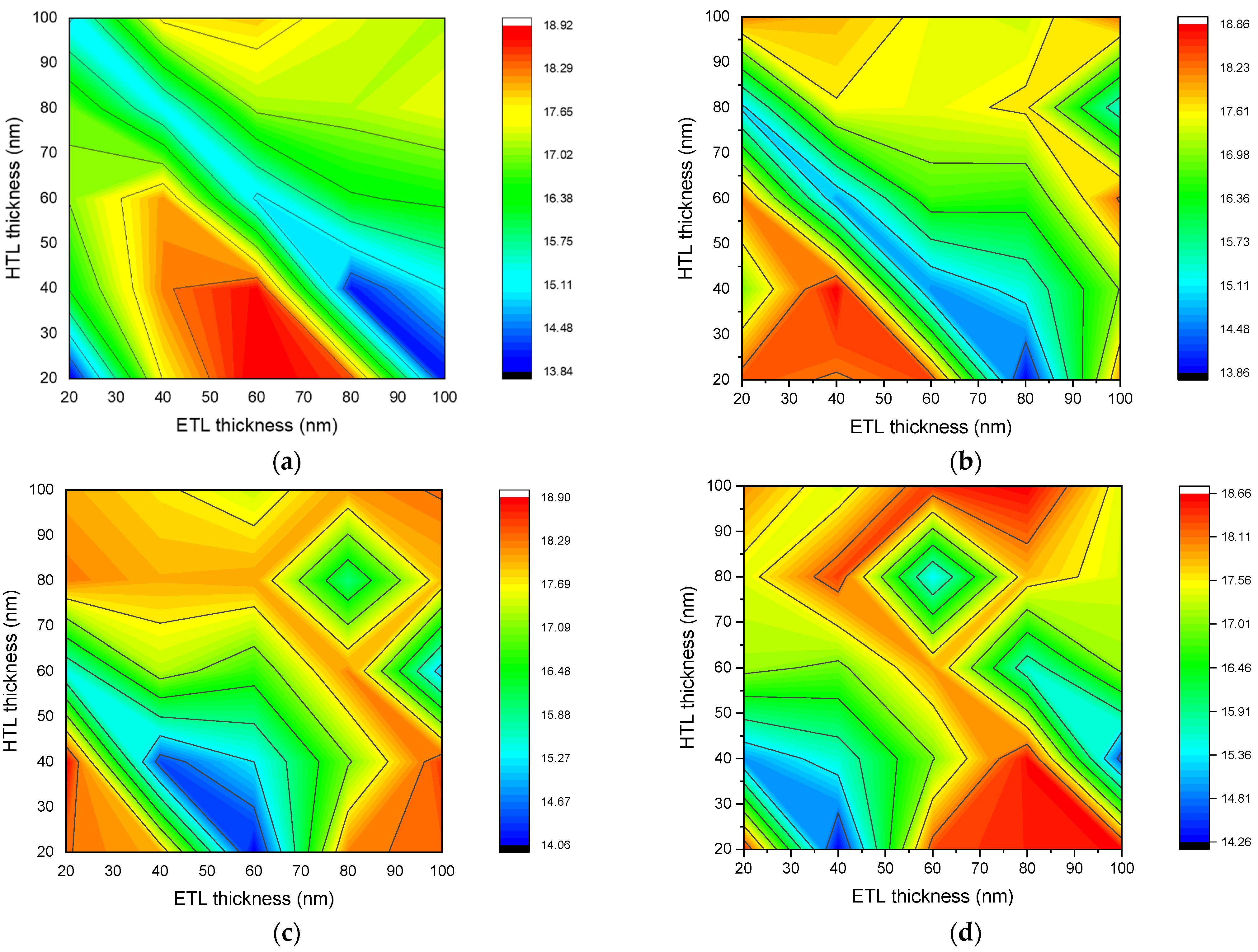
3.4. Output Power
4. Conclusions
Author Contributions
Funding
Institutional Review Board Statement
Informed Consent Statement
Data Availability Statement
Conflicts of Interest
References
- Solar Power Generation. Available online: https://ourworldindata.org/grapher/solar-energy-consumption?tab=chart (accessed on 7 July 2022).
- Ali, A.; El-Mellouhi, F.; Mitra, A.; Aïssa, B. Research progress of plasmonic nanostructure-enhanced photovoltaic solar cells. Nanomaterials 2022, 12, 788. [Google Scholar] [CrossRef]
- Xu, Y.; Gong, T.; Munday, J.N. The generalized shockley-queisser limit for nanostructured solar cells. Sci. Rep. 2015, 5, 13536. [Google Scholar] [CrossRef]
- Giannouli, M. Current status of emerging PV technologies: A comparative study of dye-sensitized, organic, and perovskite solar cells. Int. J. Photoenergy 2021, 2021, 6692858. [Google Scholar] [CrossRef]
- Pasquini, L. Nanostructured materials for energy storage and conversion. Nanomaterials 2022, 12, 1583. [Google Scholar] [CrossRef] [PubMed]
- Extance, A. The reality behind solar power’s next star material. Nature 2019, 570, 429–432. [Google Scholar] [CrossRef] [Green Version]
- Maafa, I.M. All-inorganic perovskite solar cells: Recent advancements and challenges. Nanomaterials 2022, 12, 1651. [Google Scholar] [CrossRef] [PubMed]
- Yin, W.J.; Yang, J.H.; Kang, J.; Yan, Y.; Wei, S.H. Halide perovskite materials for solar cells: A theoretical review. J. Mater. Chem. A 2015, 3, 8926–8942. [Google Scholar] [CrossRef]
- Min, H.; Lee, D.Y.; Kim, J.; Kim, G.; Lee, K.S.; Kim, J.; Paik, M.J.; Kim, Y.K.; Kim, K.S.; Kim, M.G.; et al. Perovskite solar cells with atomically coherent interlayers on SnO2 electrodes. Nature 2021, 598, 444–450. [Google Scholar] [CrossRef]
- Sha, W.E.I.; Ren, X.; Chen, L.; Choy, W.C.H. The efficiency limit of CH3NH3PbI3 perovskite solar cells. Appl. Phys. Lett. 2015, 106, 221104. [Google Scholar] [CrossRef] [Green Version]
- Babayigit, A.; Ethirajan, A.; Muller, M.; Conings, B. Toxicity of organometal halide perovskite solar cells. Nat. Mater. 2016, 15, 247–251. [Google Scholar] [CrossRef]
- Park, H.H. Efficient and stable perovskite solar cells based on inorganic hole transport materials. Nanomaterials 2021, 12, 112. [Google Scholar] [CrossRef] [PubMed]
- Conings, B.; Drijkoningen, J.; Gauquelin, N.; Babayigit, A.; D’Haen, J.; D’Olieslaeger, L.; Ethirajan, A.; Verbeeck, J.; Manca, J.; Mosconi, E.; et al. Intrinsic thermal instability of methylammonium lead trihalide perovskite. Adv. Energy Mater. 2015, 5, 1500477. [Google Scholar] [CrossRef]
- Eperon, G.E.; Stranks, S.D.; Menelaou, C.; Johnston, M.B.; Herz, L.M.; Snaith, H.J. Formamidinium lead trihalide: A broadly tunable perovskite for efficient planar heterojunction solar cells. Energy Environ. Sci. 2014, 7, 982–988. [Google Scholar] [CrossRef]
- Kim, T.; Lim, J.; Song, S. Recent progress and challenges of electron transport layers in organic—Inorganic perovskite solar cells. Energies 2020, 13, 5572. [Google Scholar] [CrossRef]
- Li, S.; Cao, Y.L.; Li, W.H.; Bo, Z.S. A brief review of hole transporting materials commonly used in perovskite solar cells. Rare Metals 2021, 40, 2712–2729. [Google Scholar] [CrossRef]
- Jhou, J.C.; Gaurav, A.; Chang, C.H.; Lin, C.F. Enhanced efficiency of semitransparent perovskite solar cells via double-sided sandwich evaporation technique for four terminal perovskite-silicon tandem application. Nanomaterials 2022, 12, 1569. [Google Scholar] [CrossRef]
- Futscher, M.H.; Ehrler, B. Efficiency limit of perovskite/si tandem solar cells. ACS Energy Lett. 2016, 1, 863–868. [Google Scholar] [CrossRef] [Green Version]
- Elsmani, M.I.; Fatima, N.; Jallorina, M.P.A.; Sepeai, S.; Su’ait, M.S.; Ludin, N.A.; Teridi, M.A.M.; Sopian, K.; Ibrahim, M.A. Recent issues and configuration factors in perovskite-silicon tandem solar cells towards large scaling production. Nanomaterials 2021, 11, 3186. [Google Scholar] [CrossRef]
- Gulomov, J.; Aliev, R. Analyzing periodical textured silicon solar cells by the TCAD modeling. Sci. Tech. J. Inf. Technol. Mech. Opt. 2021, 21, 626–632. [Google Scholar] [CrossRef]
- Gulomov, J.; Aliev, R. The way of the increasing two times the efficiency of silicon solar cell. Phys. Chem. Solid State 2021, 22, 756–760. [Google Scholar] [CrossRef]
- Islam, M.B.; Yanagida, M.; Shirai, Y.; Nabetani, Y.; Miyano, K. Highly stable semi-transparent MAPbI3 perovskite solar cells with operational output for 4000 h. Sol. Energy Mater. Sol. Cells 2019, 195, 323–329. [Google Scholar] [CrossRef]
- Prosa, M.; Tessarolo, M.; Bolognesi, M.; Margeat, O.; Gedefaw, D.; Gaceur, M.; Videlot-Ackermann, C.; Andersson, M.R.; Muccini, M.; Seri, M.; et al. Enhanced ultraviolet stability of air-processed polymer solar cells by al doping of the ZnO interlayer. ACS Appl. Mater. Interfaces 2016, 8, 1635–1643. [Google Scholar] [CrossRef] [PubMed] [Green Version]
- Gulomov, J.; Aliev, R. Influence of the angle of incident light on the performance of textured silicon solar cells. J. Nano-Electron. Phys. 2021, 13, 06036-1–06036-5. [Google Scholar] [CrossRef]
- Elrashidi, A.; Elleithy, K. High-efficiency crystalline silicon-based solar cells using textured TiO2 layer and plasmonic nanoparticles. Nanomaterials 2022, 12, 1589. [Google Scholar] [CrossRef] [PubMed]
- Ussembayev, Y.Y.; Zawacka, N.K.; Strubbe, F.; Hens, Z.; Neyts, K. Waveguiding of photoluminescence in a layer of semiconductor nanoparticles. Nanomaterials 2021, 11, 683. [Google Scholar] [CrossRef]
- Abduvohidov, M.K.; Aliev, R.; Gulomov, J. A study of the influence of the base thickness on photoelectric parameter of silicon solar cells with the new TCAD algorithms. Sci. Tech. J. Inf. Technol. Mech. Opt. 2021, 21, 774–784. [Google Scholar] [CrossRef]
- Gulomov, J.; Aliev, R.; Urmanov, B. Effect of the Thickness on Photoelectric Parameters of a Textured Silicon Solar Cell. J. Surf. Investig. 2022, 16, 416–420. [Google Scholar] [CrossRef]
- Gulomov, J.; Aliev, R. Study of the temperature coefficient of the main photoelectric parameters of silicon solar cells with various nanoparticles. J. Nano-Electron. Phys. 2021, 13, 04033. [Google Scholar] [CrossRef]
- Sermuksnis, E.; Ramonas, M.; Liberis, J.; Matulionis, A.; Avrutin, V.; Liu, H.; Izyumskaya, N.; Ozgur, U.; Morkoc, H. Electron energy relaxation in wurtzite ZnO and GaN. In Proceedings of the 2013 22nd International Conference on Noise and Fluctuations, ICNF 2013, Montpellier, France, 24–28 June 2013. [Google Scholar] [CrossRef]
- Janotti, A.; van de Walle, C.G. Fundamentals of zinc oxide as a semiconductor. Rep. Prog. Phys. 2009, 72, 126501. [Google Scholar] [CrossRef] [Green Version]
- Song, Y.L.; Zhang, T.J.; Du, H.J.; Ji, P.F.; Li, Y.; Zhou, F.Q. Synthesis, structures and temperature-dependent photoluminescence from ZnO nano/micro-rods on Zn foil. Mater. Lett. 2016, 176, 139–142. [Google Scholar] [CrossRef]
- Ellmer, K.; Mientus, R. Carrier transport in polycrystalline transparent conductive oxides: A comparative study of zinc oxide and indium oxide. Thin Solid Films 2008, 516, 4620–4627. [Google Scholar] [CrossRef] [Green Version]
- Muchahary, D.; Maity, S.; Metya, S.K. Modelling and analysis of temperature-dependent carrier lifetime and surface recombination velocity of Si–ZnO heterojunction thin film solar cell. Micro Nano Lett. 2019, 14, 399–403. [Google Scholar] [CrossRef]
- Hirasawa, M.; Ishihara, T.; Goto, T.; Uchida, K.; Miura, N. Magnetoabsorption of the lowest exciton in perovskite-type compound (CH3NH3)PbI3. Phys. B Condens. Matter 1994, 201, 427–430. [Google Scholar] [CrossRef]
- Zhao, T.; Shi, W.; Xi, J.; Wang, D.; Shuai, Z. Intrinsic and extrinsic charge transport in CH3NH3PbI3 perovskites predicted from first-principles. Sci. Rep. 2016, 6, 19968. [Google Scholar] [CrossRef]
- Landi, G.; Neitzert, H.C.; Barone, C.; Mauro, C.; Lang, F.; Albrecht, S.; Rech, B.; Pagano Landi, S.G.; Neitzert, H.C.; Barone, C.; et al. Correlation between electronic defect states distribution and device performance of perovskite solar cells. Adv. Sci. 2017, 4, 1700183. [Google Scholar] [CrossRef]
- Zhou, Q.; Jiao, D.; Fu, K.; Wu, X.; Chen, Y.; Lu, J.; Yang, S.-E. Two-dimensional device modeling of CH3NH3PbI3 based planar heterojunction perovskite solar cells. Sol. Energy 2016, 123, 51–56. [Google Scholar] [CrossRef]
- Motta, C.; El-Mellouhi, F.; Sanvito, S. Charge carrier mobility in hybrid halide perovskites. Sci. Rep. 2015, 5, 12746. [Google Scholar] [CrossRef]
- Casas, G.A.; Cappelletti, M.A.; Cédola, A.P.; Soucase, B.M.; Peltzer y Blancá, E.L. Analysis of the power conversion efficiency of perovskite solar cells with different materials as hole-transport layer by numerical simulations. Superlattices Microstruct. 2017, 107, 136–143. [Google Scholar] [CrossRef]
- ElAnzeery, H.; El Daif, O.; Buffière, M.; Oueslati, S.; ben Messaoud, K.; Agten, D.; Brammertz, G.; Guindi, R.; Kniknie, B.; Meuris, M.; et al. Refractive index extraction and thickness optimization of Cu2ZnSnSe4 thin film solar cells. Phys. Status Solidi 2015, 212, 1984–1990. [Google Scholar] [CrossRef]
- Palmstrom, A.F.; Häusele, J.; Carpenter, J.; Bush, K.A.; Mcgehee, M.D.; Manzoor, S.; Bent, S.F.; Holman, Z.C.; Yu, Z.J. Optical modeling of wide-bandgap perovskite and perovskite/silicon tandem solar cells using complex refractive indices for arbitrary-bandgap perovskite absorbers. Opt. Express 2018, 26, 27441–27460. [Google Scholar] [CrossRef]
- Löper, P.; Stuckelberger, M.; Niesen, B.; Werner, J.; Filipič, M.; Moon, S.J.; Yum, J.H.; Topič, M.; de Wolf, S.; Ballif, C. Complex refractive index spectra of CH3NH3PbI3 perovskite thin films determined by spectroscopic ellipsometry and spectrophotometry. J. Phys. Chem. Lett. 2015, 6, 66–71. [Google Scholar] [CrossRef] [PubMed]
- Gulomov, J.; Aliev, R. Numerical analysis of the effect of illumination intensity on photoelectric parameters of the silicon solar cell with various metal nanoparticles. Nanosyst. Phys. Chem. Math. 2021, 12, 569–574. [Google Scholar] [CrossRef]
- Kirchartz, T.; Staub, F.; Rau, U. Impact of photon recycling on the open-circuit voltage of metal halide perovskite solar cells. ACS Energy Lett. 2016, 1, 731–739. [Google Scholar] [CrossRef]
- Rau, U.; Paetzold, U.W.; Kirchartz, T. Thermodynamics of light management in photovoltaic devices. Phys. Rev. B-Condens. Matter Mater. Phys. 2014, 90, 035211. [Google Scholar] [CrossRef] [Green Version]
- Kirchartz, T.; Rau, U. What makes a good solar cell? Adv. Energy Mater. 2018, 8, 1703385. [Google Scholar] [CrossRef] [Green Version]
- Qarony, W.; Jui, Y.A.; Das, G.M.; Mohsin, T.; Hossain, M.I.; Islam, S.N. Optical analysis in CH3NH3PbI3 and CH3NH3PbI2Cl based thin-film perovskite solar cell. Am. J. Energy Res. 2015, 3, 19–24. [Google Scholar] [CrossRef]
- Burkhard, G.F.; Hoke, E.T.; McGehee, M.D. Accounting for interference, scattering, and electrode absorption to make accurate internal quantum efficiency measurements in organic and other thin solar cells. Adv. Mater. 2010, 22, 3293–3297. [Google Scholar] [CrossRef]
- Peng, J.; Kremer, F.; Walter, D.; Wu, Y.; Ji, Y.; Xiang, J.; Liu, W.; Duong, T.; Shen, H.; Lu, T.; et al. Centimetre-scale perovskite solar cells with fill factors of more than 86 per cent. Nature 2022, 601, 573–578. [Google Scholar] [CrossRef]
- Green, M.A. Accuracy of analytical expressions for solar cell fill factors. Sol. Cells 1982, 7, 337–340. [Google Scholar] [CrossRef]
- Wu, N.; Wu, Y.; Walter, D.; Shen, H.; Duong, T.; Grant, D.; Barugkin, C.; Fu, X.; Peng, J.; White, T.; et al. Identifying the cause of voltage and fill factor losses in perovskite solar cells by using luminescence measurements. Energy Technol. 2017, 5, 1827–1835. [Google Scholar] [CrossRef] [Green Version]
- Saeed, M.A.; Cheng, S.; Biswas, S.; Kim, S.H.; Kwon, S.K.; Kim, H.; Kim, Y.H.; Shim, J.W. Remarkably high performance of organic photovoltaic devices with 3,9-bis(2-methylene-(3-(1,1-dicyanomethylene)-indanone))-5,5,11,11-tetrakis(4-hexyl meta-phenyl)-dithieno [2,3-d:2′,3′-d′]-s-indaceno [1,2-b:5,6-b′]dithiophene)-ethylhexyloxy] photoactive acceptor under halogen light illumination. J. Power Sources 2022, 518, 230782. [Google Scholar] [CrossRef]
- Kim, S.H.; Park, C.H.; Saeed, M.A.; Ko, D.H.; Lee, J.H.; Shim, J.W. β-cyclodextrin–polyacryloyl hydrazide-based surface modification for efficient electron-collecting electrodes of indoor organic photovoltaics. J. Mater. Res. Technol. 2022, 16, 1659–1666. [Google Scholar] [CrossRef]
- Saeed, M.A.; Kang, H.C.; Yoo, K.; Asiam, F.K.; Lee, J.J.; Shim, J.W. Cosensitization of metal-based dyes for high-performance dye-sensitized photovoltaics under ambient lighting conditions. Dyes Pigments 2021, 194, 109624. [Google Scholar] [CrossRef]


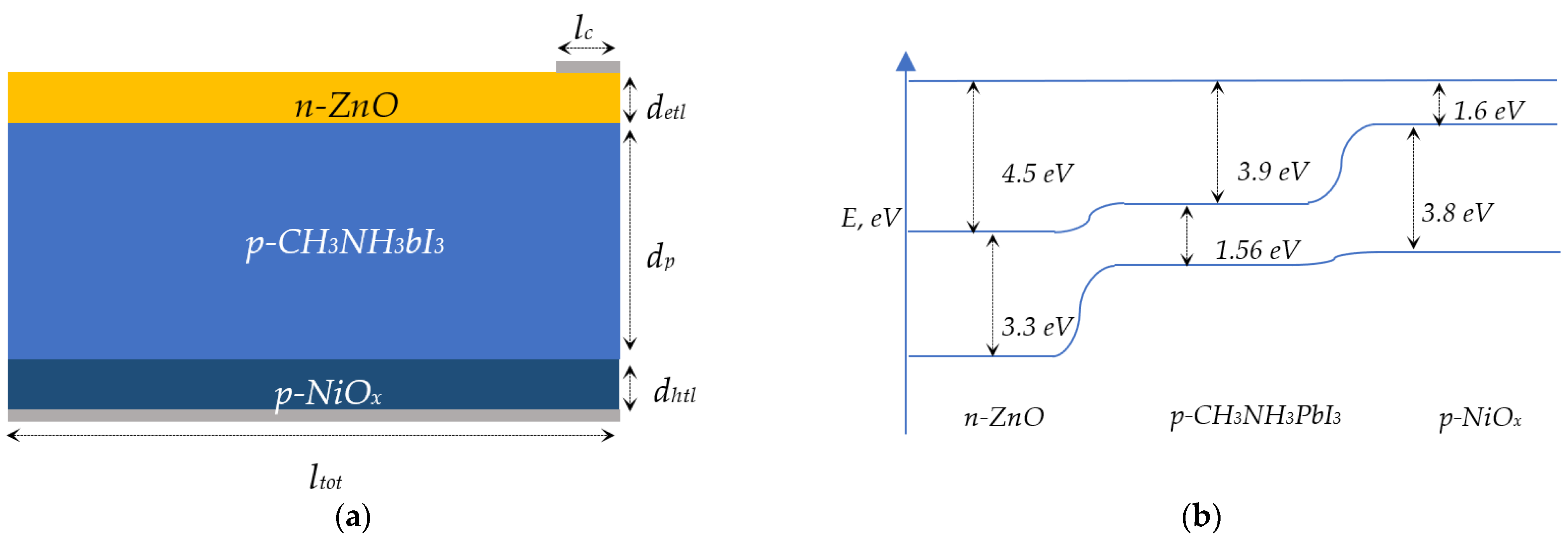
| Parameters | ZnO (Al Doped) | CH3NH3PbI3 | NiOx |
|---|---|---|---|
| Eg, eV | 3.3 | 1.56 | 3.8 |
| χ, eV | 4.5 | 3.9 | 1.6 |
| Nc, sm−3 | 2.2 × 10¹⁸ | 2.2 × 10¹⁸ | 1 × 10¹⁸ |
| Nv, sm−3 | 1.8 × 10¹⁹ | 1.8 × 10¹⁹ | 1 × 10¹⁸ |
| μe, sm2/Vs | 50 | 2.5 | 2.8 |
| μh, sm2/Vs | 5 | 5 | 2.8 |
| ε | 8.5 | 6.5 | 11 |
| τwe, ps | 0.84 | 0.33 | - |
| τwh, ps | 0.15 | 1.87 | - |
| Ie, eV | 0.054 | 0.08 | 0.3 |
Publisher’s Note: MDPI stays neutral with regard to jurisdictional claims in published maps and institutional affiliations. |
© 2022 by the authors. Licensee MDPI, Basel, Switzerland. This article is an open access article distributed under the terms and conditions of the Creative Commons Attribution (CC BY) license (https://creativecommons.org/licenses/by/4.0/).
Share and Cite
Gulomov, J.; Accouche, O.; Aliev, R.; Neji, B.; Ghandour, R.; Gulomova, I.; Azab, M. Geometric Optimization of Perovskite Solar Cells with Metal Oxide Charge Transport Layers. Nanomaterials 2022, 12, 2692. https://doi.org/10.3390/nano12152692
Gulomov J, Accouche O, Aliev R, Neji B, Ghandour R, Gulomova I, Azab M. Geometric Optimization of Perovskite Solar Cells with Metal Oxide Charge Transport Layers. Nanomaterials. 2022; 12(15):2692. https://doi.org/10.3390/nano12152692
Chicago/Turabian StyleGulomov, Jasurbek, Oussama Accouche, Rayimjon Aliev, Bilel Neji, Raymond Ghandour, Irodakhon Gulomova, and Marc Azab. 2022. "Geometric Optimization of Perovskite Solar Cells with Metal Oxide Charge Transport Layers" Nanomaterials 12, no. 15: 2692. https://doi.org/10.3390/nano12152692
APA StyleGulomov, J., Accouche, O., Aliev, R., Neji, B., Ghandour, R., Gulomova, I., & Azab, M. (2022). Geometric Optimization of Perovskite Solar Cells with Metal Oxide Charge Transport Layers. Nanomaterials, 12(15), 2692. https://doi.org/10.3390/nano12152692