
Reset First Resistive Switching in Ni1−xO Thin Films as Charge Transfer Insulator Deposited by Reactive RF Magnetron Sputtering


Abstract
:1. Introduction
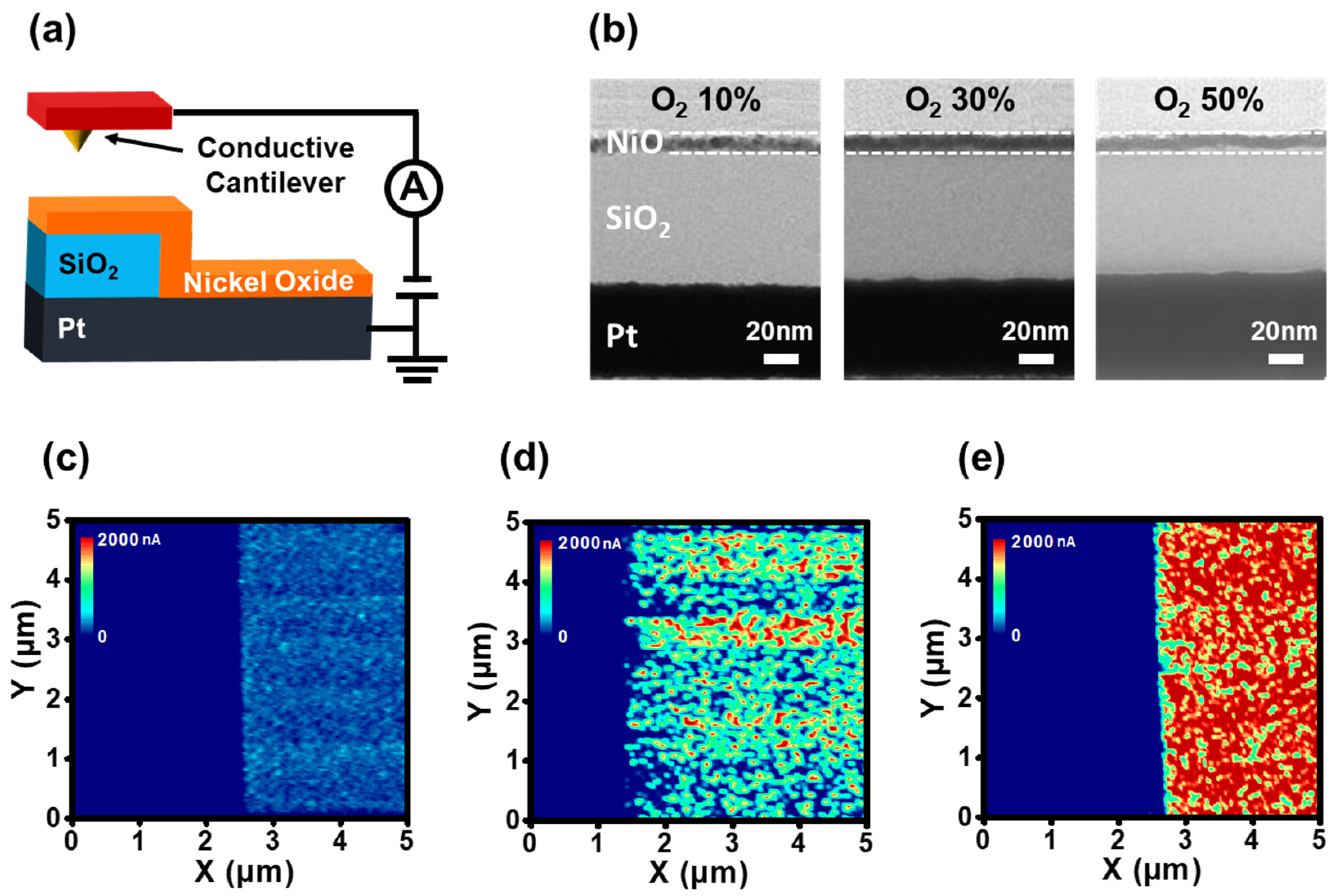
2. Experimental
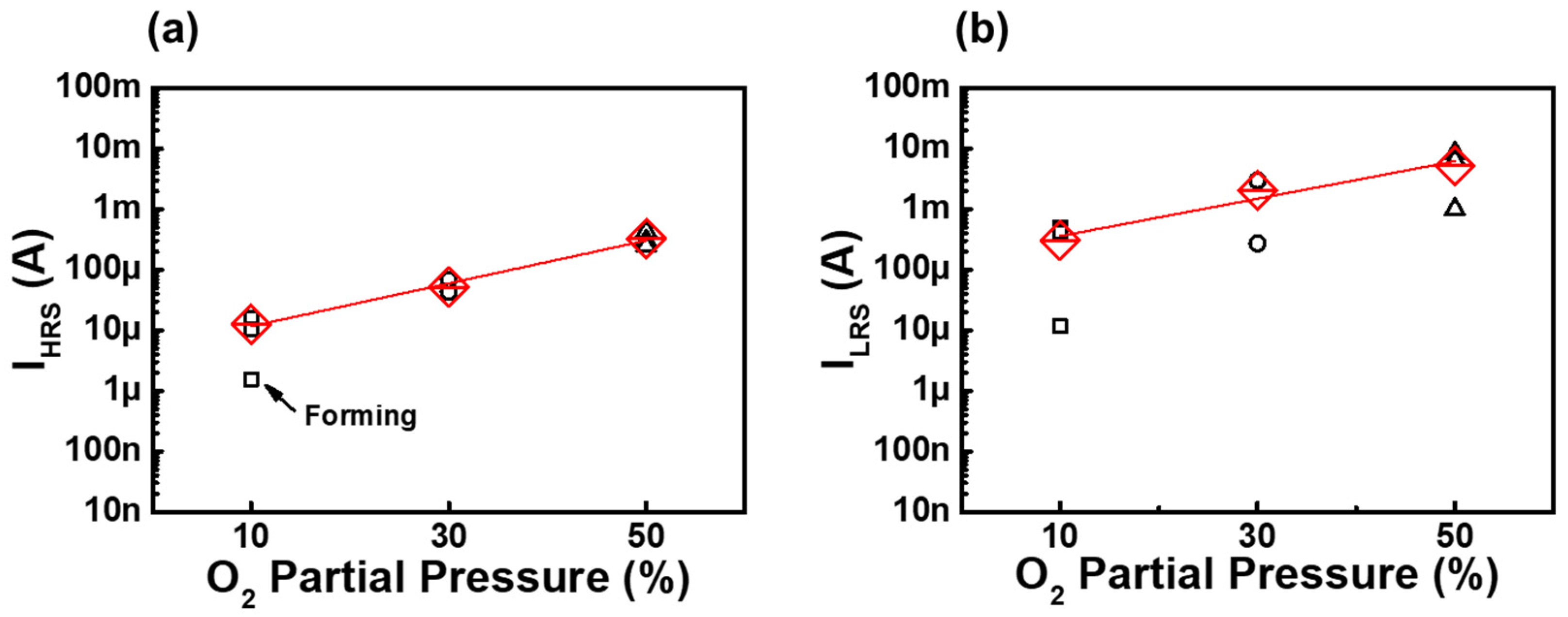
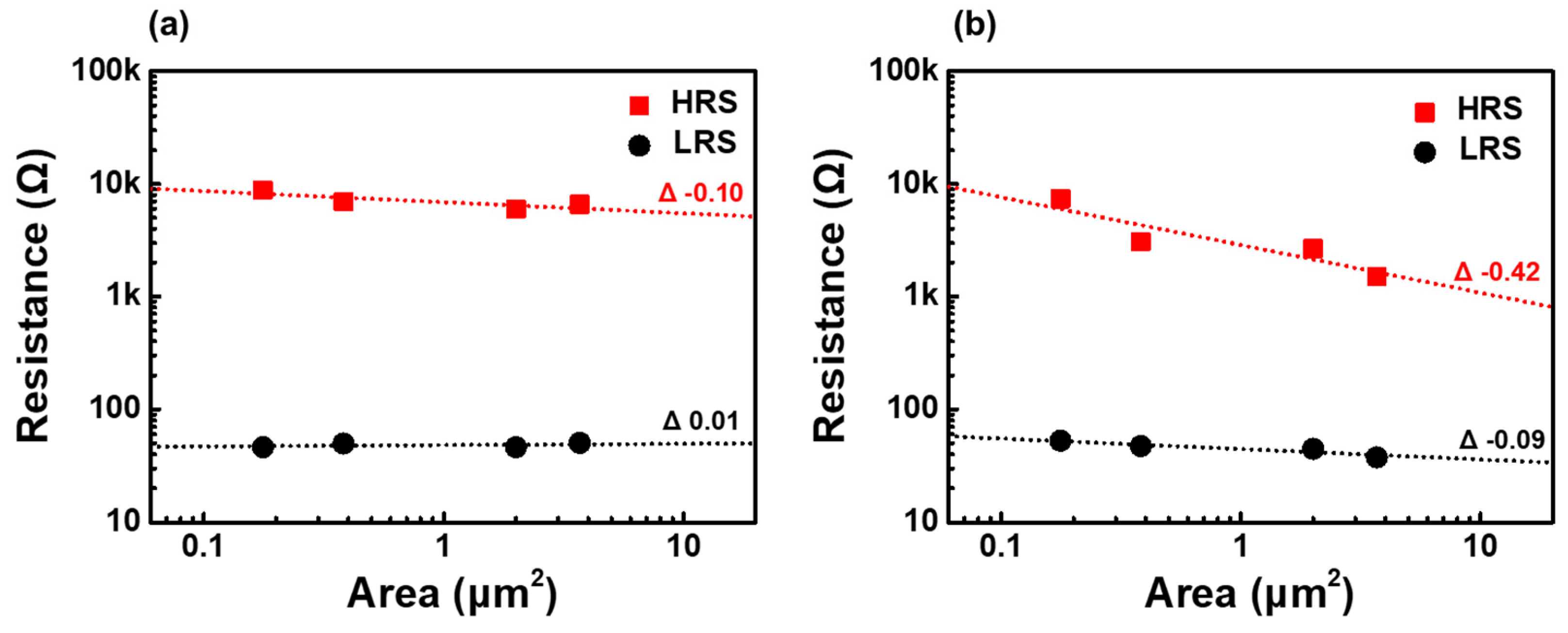
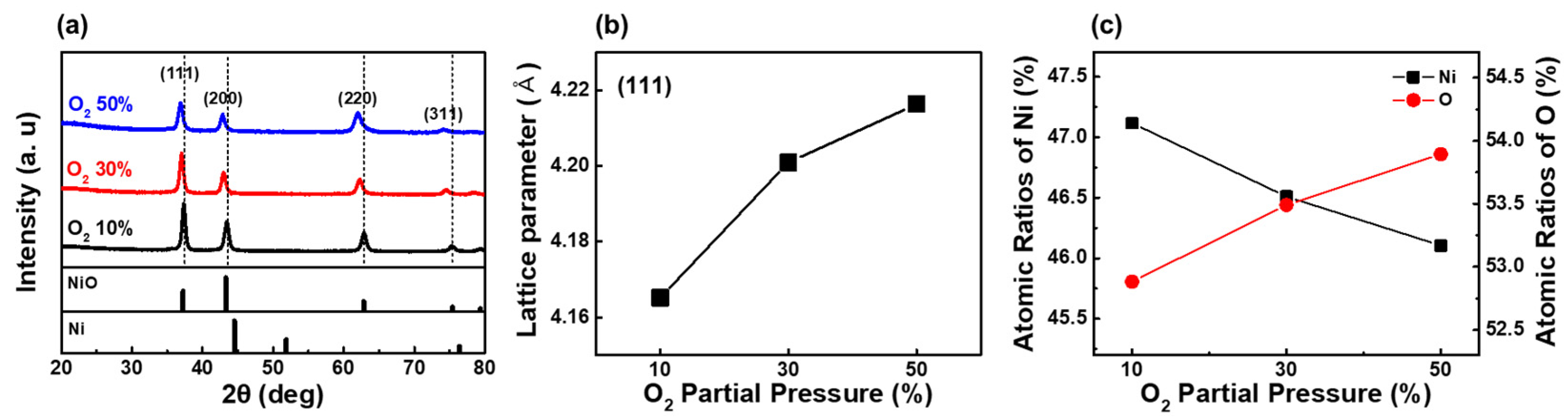
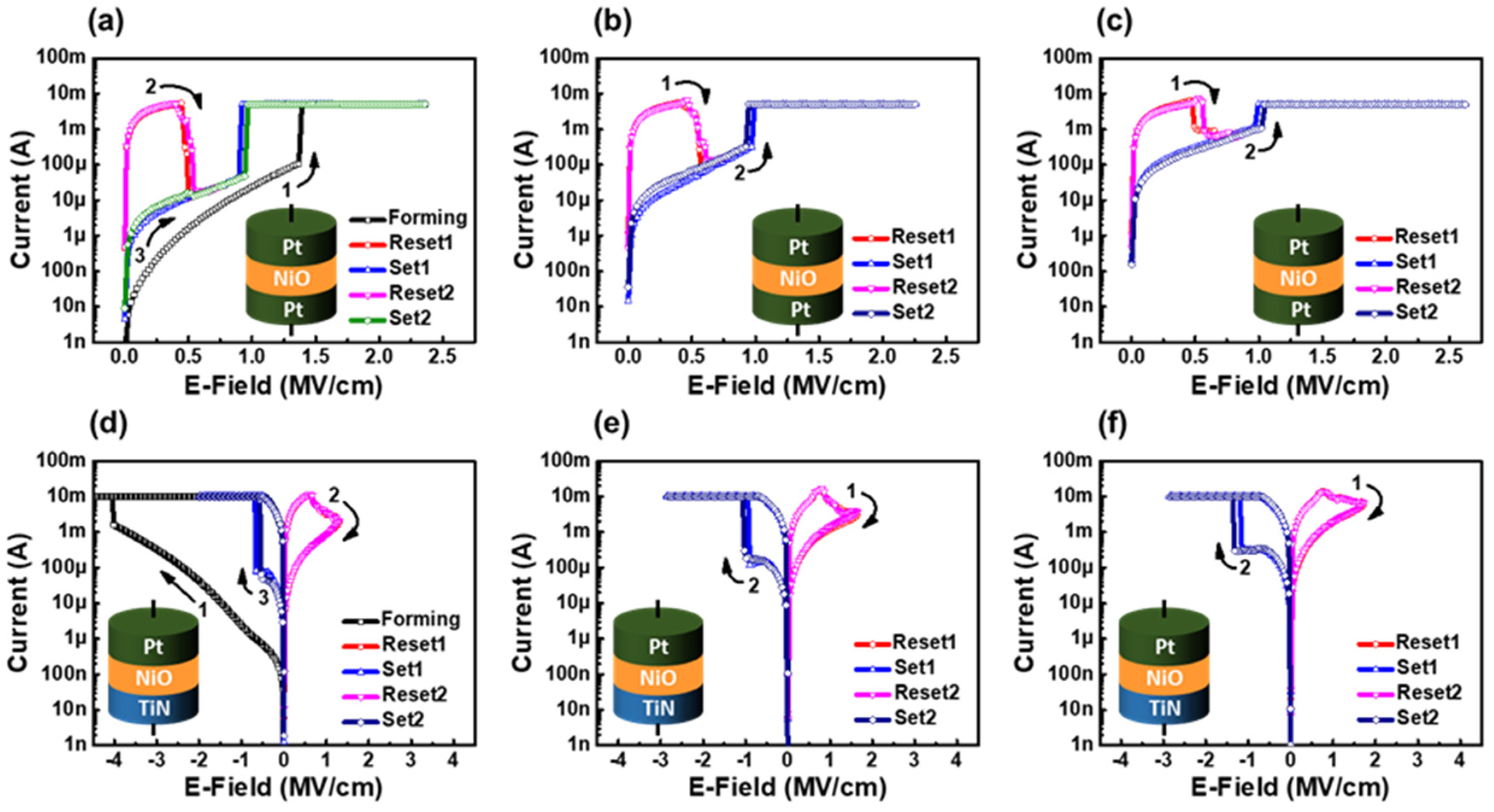
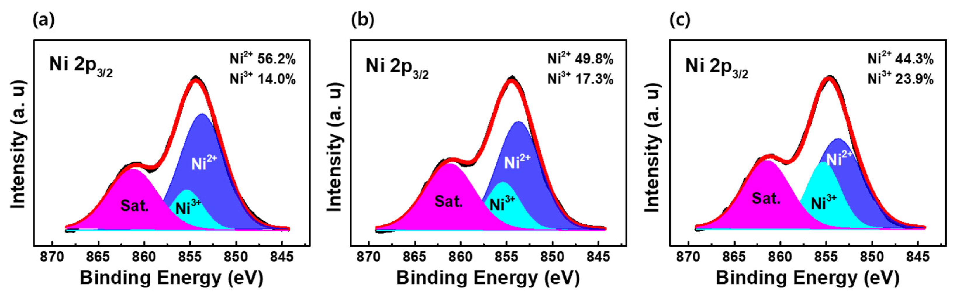
3. Results and Discussion
4. Conclusions
Supplementary Materials
Author Contributions
Funding
Conflicts of Interest
References
- Zahoor, F.; Zulkifli, T.Z.A.; Khanday, F.A. Resistive Random access Memory (RRAM): An Overview of Materials, Switching Mechanism, Performance, Multilevel Cell (mlc) Storage, Modeling, and Applications. Nanoscale Res. Lett. 2020, 15, 90. [Google Scholar] [CrossRef] [PubMed]
- Wang, H.; Yan, X. Overview of Resistive Random access Memory (RRAM): Materials, Filament Mechanisms, Performance Optimization, and Prospects. Phys. Status Solidi (RRL)–Rapid Res. Lett. 2019, 13, 1900073. [Google Scholar] [CrossRef]
- Wang, L.; Yang, C.; Wen, J.; Gai, S. Emerging Nonvolatile Memories to Go Beyond Scaling Limits of Conventional CMOS Nanodevices. J. Nanomater. 2014, 2014, 927696. [Google Scholar] [CrossRef]
- Pan, F.; Gao, S.; Chen, C.; Song, C.; Zeng, F. Recent progress in resistive random access memories: Materials, switching mechanisms, and performance. Mater. Sci. Eng.: R: Rep. 2014, 83, 1–59. [Google Scholar] [CrossRef]
- Wong, H.S.P.; Lee, H.-Y.; Yu, S.; Chen, Y.-S.; Wu, Y.; Chen, P.-S.; Lee, B.; Chen, F.T.; Tsai, M.-J. Metal–Oxide RRAM. Proc. IEEE 2012, 100, 1951–1970. [Google Scholar] [CrossRef]
- Quan, X.-T.; Zhu, H.-C.; Cai, H.-T.; Zhang, J.-Q.; Wang, X.-J. Resistive Switching Behavior in Amorphous Aluminum Oxide Film Grown by Chemical Vapor Deposition. Chin. Phys. Lett. 2014, 31, 078101. [Google Scholar] [CrossRef]
- Rodrigues, A.; Santos, Y.; Rodrigues, C.; Macêdo, M. Al2O3 thin film multilayer structure for application in RRAM devices. Solid-State Electron. 2018, 149, 1–5. [Google Scholar] [CrossRef]
- Lin, Y.S.; Zeng, F.; Tang, S.G.; Liu, H.Y.; Chen, C.; Gao, S.; Wang, Y.G.; Pan, F. Resistive switching mechanisms relating to oxygen vacancies migration in both interfaces in Ti/HfOx/Pt memory devices. J. Appl. Phys. 2013, 113, 064510. [Google Scholar] [CrossRef]
- Raghavan, N.; Fantini, A.; Degraeve, R.; Roussel, P.; Goux, L.; Govoreanu, B.; Wouters, D.; Groeseneken, G.; Jurczak, M. Statistical insight into controlled forming and forming free stacks for HfOx RRAM. Microelectron. Eng. 2013, 109, 177–181. [Google Scholar] [CrossRef]
- Ku, B.; Abbas, Y.; Sokolov, A.S.; Choi, C. Interface engineering of ALD HfO2-based RRAM with Ar plasma treatment for reliable and uniform switching behaviors. J. Alloy. Compd. 2018, 735, 1181–1188. [Google Scholar] [CrossRef]
- Seo, S.; Lee, M.-J.; Seo, D.H.; Jeoung, E.J.; Suh, D.-S.; Joung, Y.S.; Yoo, I.K.; Hwang, I.R.; Kim, S.H.; Byun, I.S.; et al. Reproducible resistance switching in polycrystalline NiO films. Appl. Phys. Lett. 2004, 85, 5655–5657. [Google Scholar] [CrossRef]
- Yoshida, C.; Kinoshita, K.; Yamasaki, T.; Sugiyama, Y. Direct observation of oxygen movement during resistance switching in NiO/Pt film. Appl. Phys. Lett. 2008, 93, 042106. [Google Scholar] [CrossRef]
- Liu, C.-Y.; Ho, J.-Y.; Huang, J.-J.; Wang, H.-Y. Transient Current of Resistive Switching of a NiO$_{x}$ Resistive Memory. Jpn. J. Appl. Phys. 2012, 51, 041101. [Google Scholar] [CrossRef]
- Alagoz, H.S.; Tan, L.; Jung, J.; Chow, K.H. Switching characteristics of NiOx crossbar arrays driven by low-temperature electroforming. Appl. Phys. A 2021, 127, 499. [Google Scholar] [CrossRef]
- Yang, J.J.; Inoue, I.H.; Mikolajick, T.; Hwang, C.S. Metal oxide memories based on thermochemical and valence change mechanisms. MRS Bull. 2012, 37, 131–137. [Google Scholar] [CrossRef]
- Trapatseli, M.; Khiat, A.; Cortese, S.; Serb, A.; Carta, D.; Prodromakis, T. Engineering the switching dynamics of TiOx-based RRAM with Al doping. J. Appl. Phys. 2016, 120, 025108. [Google Scholar] [CrossRef]
- Chen, C.; Song, C.; Yang, J.; Zeng, F.; Pan, F. Oxygen migration induced resistive switching effect and its thermal stability in W/TaOx/Pt structure. Appl. Phys. Lett. 2012, 100, 253509. [Google Scholar] [CrossRef]
- Jiang, Y.; Tan, C.C.; Li, M.H.; Fang, Z.; Weng, B.B.; He, W.; Zhuo, V.Y.-Q. Forming-Free TaOxBased RRAM Device with Low Operating Voltage and High On/Off Characteristics. ECS J. Solid State Sci. Technol. 2015, 4, N137–N140. [Google Scholar] [CrossRef]
- Hanzig, F.; Mähne, H.; Veselý, J.; Wylezich, H.; Slesazeck, S.; Leuteritz, A.; Zschornak, M.; Motylenko, M.; Klemm, V.; Mikolajick, T.; et al. Effect of the stoichiometry of niobium oxide on the resistive switching of Nb 2 O 5 based metal–insulator–metal stacks. J. Electron Spectrosc. Relat. Phenom. 2015, 202, 122–127. [Google Scholar] [CrossRef]
- Kundozerova, T.V.; Grishin, A.M.; Stefanovich, G.B.; Velichko, A.A. Anodic Nb2O5 Nonvolatile RRAM. IEEE Trans. Electron Devices 2012, 59, 1144–1148. [Google Scholar] [CrossRef]
- Asamitsu, A.; Tomioka, Y.; Kuwahara, H.; Tokura, Y. Current switching of resistive states in magnetoresistive manganites. Nature 1997, 388, 50–52. [Google Scholar] [CrossRef]
- Lashkare, S.; Chouhan, S.; Chavan, T.; Bhat, A.; Kumbhare, P.; Ganguly, U. PCMO RRAM for Integrate-and-Fire Neuron in Spiking Neural Networks. IEEE Electron Device Lett. 2018, 39, 484–487. [Google Scholar] [CrossRef]
- Panwar, N.; Ganguly, U. Variability assessment and mitigation by predictive programming in Pr 0.7 Ca 0.3 MnO 3 based RRAM. In Proceedings of the 2015 73rd Annual Device Research Conference (DRC), Columbus, OH, USA, 21–24 June 2015; pp. 141–142. [Google Scholar]
- Depla, D.; Mahieu, S. Reactive Sputter Deposition; Springer: Berlin/Heidelberg, Germany, 2008. [Google Scholar]
- Stognij, A.; Sharko, S.; Serokurova, A.; Trukhanov, S.; Panina, L.; Ketsko, V.; Dyakonov, V.; Szymczak, H.; Vinnik, D.; Gudkova, S. Preparation and investigation of the magnetoelectric properties in layered cermet structures. Ceram. Int. 2019, 45, 13030–13036. [Google Scholar] [CrossRef]
- Sharko, S.A.; Serokurova, A.I.; Novitskii, N.N.; Ketsko, V.A.; Smirnova, M.N.; Almuqrin, A.H.; Sayyed, M.I.; Trukhanov, S.V.; Trukhanov, A.V. A New Approach to the Formation of Nanosized Gold and Beryllium Films by Ion-Beam Sputtering Deposition. Nanomaterials 2022, 12, 470. [Google Scholar] [CrossRef]
- Zubar, T.; Fedosyuk, V.; Tishkevich, D.; Kanafyev, O.; Astapovich, K.; Kozlovskiy, A.; Zdorovets, M.; Vinnik, D.; Gudkova, S.; Kaniukov, E.; et al. The Effect of Heat Treatment on the Microstructure and Mechanical Properties of 2D Nanostructured Au/NiFe System. Nanomaterials 2020, 10, 1077. [Google Scholar] [CrossRef]
- Zubar, T.I.; Fedosyuk, V.M.; Trukhanov, S.V.; Tishkevich, D.I.; Michels, D.; Lyakhov, D.; Trukhanov, A.V. Method of surface energy investigation by lateral AFM: Application to control growth mechanism of nanostructured NiFe films. Sci. Rep. 2020, 10, 14411. [Google Scholar] [CrossRef]
- George, S.M. Atomic Layer Deposition: An Overview. Chem. Rev. 2009, 110, 111–131. [Google Scholar] [CrossRef]
- Greer, J.A. History and current status of commercial pulsed laser deposition equipment. J. Phys. D Appl. Phys. 2013, 47, 34005. [Google Scholar] [CrossRef] [Green Version]
- Trukhanov, S.V.; Vasil’Ev, A.N.; Maignan, A.; Szymczak, H. Critical behavior of La0.825Sr0.175MnO2.912 anion-deficient manganite in the magnetic phase transition region. J. Exp. Theor. Phys. Lett. 2007, 85, 507–512. [Google Scholar] [CrossRef]
- Trukhanov, A.; Kostishyn, V.; Panina, L.; Korovushkin, V.; Turchenko, V.; Vinnik, D.; Yakovenko, E.; Zagorodnii, V.; Launetz, V.; Oliynyk, V.; et al. Correlation of the atomic structure, magnetic properties and microwave characteristics in substituted hexagonal ferrites. J. Magn. Magn. Mater. 2018, 462, 127–135. [Google Scholar] [CrossRef]
- Hüfner, S. Electronic structure of NiO and related 3d-transition-metal compounds. Adv. Phys. 1994, 43, 183–356. [Google Scholar] [CrossRef]
- Ferreira, L.G.; Marques, L.K.T. Band structure of NiO revisited. Mater. Sci. (Cond.-Mat. Mtrl.-Sci.) 2009. Available online: https://www.semanticscholar.org/paper/Band-structure-of-NiO-revisited-Ferreira-Teles/0d15b06260c2aff5df1c9531066bdac6f50f9145 (accessed on 26 June 2022).
- Janod, E.; Tranchant, J.; Corraze, B.; Querré, M.; Stoliar, P.; Rozenberg, M.; Cren, T.; Roditchev, D.; Phuoc, V.T.; Besland, M.-P.; et al. Resistive Switching in Mott Insulators and Correlated Systems. Adv. Funct. Mater. 2015, 25, 6287–6305. [Google Scholar] [CrossRef]
- Karolak, M.; Ulm, G.; Wehling, T.; Mazurenko, V.; Poteryaev, A.; Lichtenstein, A. Double counting in LDA+DMFT—The example of NiO. J. Electron Spectrosc. Relat. Phenom. 2010, 181, 11–15. [Google Scholar] [CrossRef] [Green Version]
- Xue, K.-H.; de Araujo, C.A.P.; Celinska, J.; McWilliams, C. A non-filamentary model for unipolar switching transition metal oxide resistance random access memories. J. Appl. Phys. 2011, 109, 091602. [Google Scholar] [CrossRef]
- Xu, N.; Liu, L.; Sun, X.; Liu, X.; Han, D.; Wang, Y.; Han, R.; Kang, J.; Yu, B. Characteristics and mechanism of conduction/set process in TiN∕ZnO∕Pt resistance switching random-access memories. Appl. Phys. Lett. 2008, 92, 232112. [Google Scholar] [CrossRef]
- Chien, F.S.-S.; Wu, Y.T.; Lai, G.L.; Lai, Y.H. Disproportionation and comproportionation reactions of resistive switching in polycrystalline NiOx films. Appl. Phys. Lett. 2011, 98, 153513. [Google Scholar] [CrossRef] [Green Version]
- Russo, U.; Ielmini, D.; Cagli, C.; Lacaita, A.L. Filament Conduction and Reset Mechanism in NiO-Based Resistive-Switching Memory (RRAM) Devices. IEEE Trans. Electron Devices 2009, 56, 186–192. [Google Scholar] [CrossRef]
- Chen, Y.S.; Kang, J.F.; Chen, B.; Gao, B.; Liu, L.F.; Liu, X.Y.; Wang, Y.Y.; Wu, L.; Yu, H.Y.; Wang, J.Y.; et al. Microscopic mechanism for unipolar resistive switching behaviour of nickel oxides. J. Phys. D Appl. Phys. 2012, 45, 65303. [Google Scholar] [CrossRef]
- Grossi, A.; Nowak, E.; Zambelli, C.; Pellissier, C.; Bernasconi, S.; Cibrario, G.; el Hajjam, K.; Crochemore, R.; Nodin, J.; Olivo, P. Fundamental variability limits of filament-based RRAM. In Proceedings of the 2016 IEEE International Electron Devices Meeting (IEDM), San Francisco, CA, USA, 3–7 December 2016; pp. 4.7.1–4.7.4. [Google Scholar]
- Fang, Z.; Yu, H.Y.; Li, X.; Singh, N.; Lo, G.Q.; Kwong, D.L. HfOx/TiOx/HfOx/TiOx Multilayer-Based Forming-Free RRAM Devices With Excellent Uniformity. IEEE Electron Device Lett. 2011, 32, 566–568. [Google Scholar] [CrossRef]
- Luo, Q.; Zhang, X.; Hu, Y.; Gong, T.; Xu, X.; Yuan, P.; Ma, H.; Dong, D.; Lv, H.; Long, S.; et al. Self-Rectifying and Forming-Free Resistive-Switching Device for Embedded Memory Application. IEEE Electron Device Lett. 2018, 39, 664–667. [Google Scholar] [CrossRef]
- Aglieri, V.; Lullo, G.; Mosca, M.; Macaluso, R.; Zaffora, A.; DI Franco, F.; Santamaria, M.; Cicero, U.L.; Razzari, L. Forming-Free and Self-Rectifying Resistive Switching Effect in Anodic Titanium Dioxide-Based Memristors. In Proceedings of the 2018 IEEE 4th International Forum on Research and Technology for Society and Industry (RTSI), Palermo, Italy, 10–13 September 2018; pp. 1–4. [Google Scholar] [CrossRef]
- De Wolf, P.; Snauwaert, J.; Clarysse, T.; Vandervorst, W.; Hellemans, L. Characterization of a point-contact on silicon using force microscopy-supported resistance measurements. Appl. Phys. Lett. 1995, 66, 1530–1532. [Google Scholar] [CrossRef]
- Alexeev, A.; Loos, J.; Koetse, M. Nanoscale electrical characterization of semiconducting polymer blends by conductive atomic force microscopy (C-AFM). Ultramicroscopy 2006, 106, 191–199. [Google Scholar] [CrossRef] [PubMed]
- Kim, D.S.; Lee, H.C. Nickel vacancy behavior in the electrical conductance of nonstoichiometric nickel oxide film. J. Appl. Phys. 2012, 112, 034504. [Google Scholar] [CrossRef]
- Chen, T.; Wang, A.; Shang, B.; Wu, Z.; Li, Y.; Wang, Y. Property modulation of NiO films grown by radio frequency magnetron sputtering. J. Alloy. Compd. 2015, 643, 167–173. [Google Scholar] [CrossRef]
- Jang, W.-L.; Lu, Y.-M.; Hwang, W.-S.; Hsiung, T.-L.; Wang, H.P. Point defects in sputtered NiO films. Appl. Phys. Lett. 2009, 94, 062103. [Google Scholar] [CrossRef]
- Lombardo, S.; Stathis, J.H.; Linder, B.P.; Pey, K.L.; Palumbo, F.; Tung, C.H. Dielectric breakdown mechanisms in gate oxides. J. Appl. Phys. 2005, 98, 121301. [Google Scholar] [CrossRef]
- Akinaga, H.; Shima, H. Resistive Random Access Memory (ReRAM) Based on Metal Oxides. Proc. IEEE 2010, 98, 2237–2251. [Google Scholar] [CrossRef]
- Liu, L.; Hou, Y.; Chen, B.; Gao, B.; Kang, J. Improved unipolar resistive switching characteristics of mixed-NiOx/NiOy-film-based resistive switching memory devices. Jpn. J. Appl. Phys. 2015, 54, 094201. [Google Scholar] [CrossRef]
- Das, N.C.; Kim, M.; Rani, J.R.; Hong, S.-M.; Jang, J.-H. Electroforming-Free Bipolar Resistive Switching Memory Based on Magnesium Fluoride. Micromachines 2021, 12, 1049. [Google Scholar] [CrossRef]
- Das, N.C.; Oh, S.-I.; Rani, J.R.; Hong, S.-M.; Jang, J.-H. Multilevel Bipolar Electroforming-Free Resistive Switching Memory Based on Silicon Oxynitride. Appl. Sci. 2020, 10, 3506. [Google Scholar] [CrossRef]
- Li, Y.-T.; Long, S.-B.; Lü, H.-B.; Liu, Q.; Wang, Q.; Wang, Y.; Zhang, S.; Lian, W.-T.; Liu, S.; Liu, M. Investigation of resistive switching behaviours in WO3-based RRAM devices. Chin. Phys. B 2011, 20, 017305. [Google Scholar] [CrossRef]
- Lee, J.; Park, J.; Jung, S.; Hwang, H. Scaling effect of device area and film thickness on electrical and reliability characteristics of RRAM. In Proceedings of the 2011 IEEE International Interconnect Technology Conference, Dresden, Germany, 8–12 May 2011; pp. 1–3. [Google Scholar]
- Park, C.; Kim, J.; Lee, K.; Oh, S.K.; Kang, H.J.; Park, N.S. Electronic, Optical and Electrical Properties of Nickel Oxide Thin Films Grown by RF Magnetron Sputtering. Appl. Sci. Converg. Technol. 2015, 24, 72–76. [Google Scholar] [CrossRef] [Green Version]
- Grosvenor, A.P.; Biesinger, M.C.; Smart, R.S.C.; McIntyre, N.S. New interpretations of XPS spectra of nickel metal and oxides. Surf. Sci. 2006, 600, 1771–1779. [Google Scholar] [CrossRef]
- McWilliams, C.R.; Celinska, J.; de Araujo, C.A.P.; Xue, K.-H. Device characterization of correlated electron random access memories. J. Appl. Phys. 2011, 109, 091608. [Google Scholar] [CrossRef]
- Kwon, D.-H.; Lee, S.R.; Choi, Y.S.; Son, S.-B.; Oh, K.H.; Char, K.; Kim, M. Observation of the Ni2 O3 phase in a NiO thin-film resistive switching system. Phys. Status Solidi (RRL)–Rapid Res. Lett. 2017, 11, 1700048. [Google Scholar] [CrossRef]


Publisher’s Note: MDPI stays neutral with regard to jurisdictional claims in published maps and institutional affiliations. |
© 2022 by the authors. Licensee MDPI, Basel, Switzerland. This article is an open access article distributed under the terms and conditions of the Creative Commons Attribution (CC BY) license (https://creativecommons.org/licenses/by/4.0/).
Share and Cite
Kim, D.-w.; Kim, T.-h.; Kim, J.-y.; Sohn, H.-c. Reset First Resistive Switching in Ni1−xO Thin Films as Charge Transfer Insulator Deposited by Reactive RF Magnetron Sputtering. Nanomaterials 2022, 12, 2231. https://doi.org/10.3390/nano12132231
Kim D-w, Kim T-h, Kim J-y, Sohn H-c. Reset First Resistive Switching in Ni1−xO Thin Films as Charge Transfer Insulator Deposited by Reactive RF Magnetron Sputtering. Nanomaterials. 2022; 12(13):2231. https://doi.org/10.3390/nano12132231
Chicago/Turabian StyleKim, Dae-woo, Tae-ho Kim, Jae-yeon Kim, and Hyun-chul Sohn. 2022. "Reset First Resistive Switching in Ni1−xO Thin Films as Charge Transfer Insulator Deposited by Reactive RF Magnetron Sputtering" Nanomaterials 12, no. 13: 2231. https://doi.org/10.3390/nano12132231
APA StyleKim, D.-w., Kim, T.-h., Kim, J.-y., & Sohn, H.-c. (2022). Reset First Resistive Switching in Ni1−xO Thin Films as Charge Transfer Insulator Deposited by Reactive RF Magnetron Sputtering. Nanomaterials, 12(13), 2231. https://doi.org/10.3390/nano12132231