Article

Graphene Oxide: Graphene Quantum Dot Nanocomposite for Better Memristic Switching Behaviors

1
HLJ Province Key Laboratories of Senior-Education for Electronic Engineering, Heilongjiang University, Harbin 150080, China
2
Research Center for Fiber Optic Sensing Technology National Local Joint Engineering, Heilongjiang University, Harbin 150080, China
Nanomaterials 2020, 10(8), 1448; https://doi.org/10.3390/nano10081448
Submission received: 27 June 2020 / Revised: 15 July 2020 / Accepted: 21 July 2020 / Published: 24 July 2020

Abstract

:
Tristable memristic switching provides the capability for multi-bit data storage. In this study, all-inorganic multi-bit memory devices were successfully manufactured by the attachment of graphene quantum dots (GQDs) onto graphene oxide (GO) through a solution-processable method. By means of doping GQDs as charge-trapping centers, the device indium-tin oxide (ITO)/GO:0.5 wt%GQDs/Ni revealed controllable memristic switching behaviors that were tunable from binary to ternary, and remarkably enhanced in contrast with ITO/GO/Ni. It was found that the device has an excellent performance in memristic switching parameters, with a SET1, SET2 and RESET voltage of −0.9 V, −1.7 V and 5.15 V, as well as a high ON2/ON1/OFF current ratio (103:102:1), and a long retention time (104 s) together with 100 successive cycles. The conduction mechanism of the binary and ternary GO-based memory cells was discussed in terms of experimental data employing a charge trapping-detrapping mechanism. The reinforcement effect of GQDs on the memristic switching of GO through cycle-to-cycle operation has been extensively investigated, offering great potential application for multi-bit data storage in ultrahigh-density, nonvolatile memory.

1. Introduction

The memristor (memory-resistor) is a fourth fundamental passive circuit element, and its resistance can drastically vary with a minor change in input [1,2]. It cannot be modeled with the capacitor (C), resistor (R), or inductor (L), not because they are fundamental, but because memristors are composite resistors that rely on active hysteresis to switch between low and high resistance states. The memristor’s potential for phenomenal computing is in no way diminished by the negative assessment of its qualifications as a fundamental device [3,4]. With remarkable features, such as scalability, low power consumption and dynamic responses, it has recently been anticipated to take a massive leap in revolutionizing the electronic circuits for nonvolatile memory and programmable logic [5,6,7].
Inorganic, polymeric, and organic materials predominantly have been found to exhibit memristor properties [8,9,10]. Most of them, nevertheless, are suitable for binary systems based on electrical bistability. Namely, the data storage capacity is limited in 2n. It is essential for developing highly integrated memory devices [11,12,13,14], that multi-bit operation is confronted with currently available commercial memory devices to allow the capacity for more than one bit (a digital state of ‘0’ or ‘1’) in a particular memory cell.
Graphene oxide (GO) is a layered material consisting of hydrophilic, oxygenated graphene sheets. The functional groups presented on the basal planes and edges of GO are reactive sites for physical/chemical bonding with polymers and alter the van der Waals interactions, preventing them from aggregation [15,16,17]. Due to their presence, GO can be stably dispersed into various polar solvents, like water. Apart from its lower cost of fabrication, higher scalability, lightweight and environment-friendly natures, the advantages of GO-based memory include features, such as flexibility, solution processing and 3D-stacking capability [18,19,20,21]. Graphene quantum dots (GQDs) bear unique properties of high electron mobility, excellent solubility and easy functionalization [22,23,24,25,26]. Particularly, carbon nanomaterials have acted as the charge trapping centers to realize the memory effect [27,28]. The memristic parameter indices, such as the ON/OFF current ratio, power consumption, retention stability and reproducibility have been effectively tunable by way of the blending approach. Considering these benefits, it is reasonable to expect GQDs doping to enhance GO as excellent memristic switching materials for multi-bit data storage.
It still needs solutions for multi-bit memory devices to surmount some technical obstacles, such as complex fabrication processes, or multilayer stacked structures [12,29,30,31,32,33]. Herein, all-inorganic memristic switching devices based on GO were fabricated by means of a simple solution-processable approach, which transformed behaviors from binary to ternary memory by doping GQDs. Fourier transform infrared (FTIR) spectroscopy, Raman spectroscopy, thermogravimetric analysis (TGA), as well as scanning electron microscopy (SEM) characterization techniques were performed for the nature assessment of GO and GO:GQDs nanocomposite system. Great efforts have been made to establish the memristic switching characteristics of GO-based nanocomposites, and to interrogate the effect of GQDs introduced into such systems. The study included an evaluation of multi-bit memristic switching behaviors and made a comparison between GO and its nanocomposites, comprising the cycle-to-cycle and device-to-device performance of indium-tin oxide (ITO)/GO/Ni and ITO/GO:GQDs/Ni devices.

2. Materials and Methods

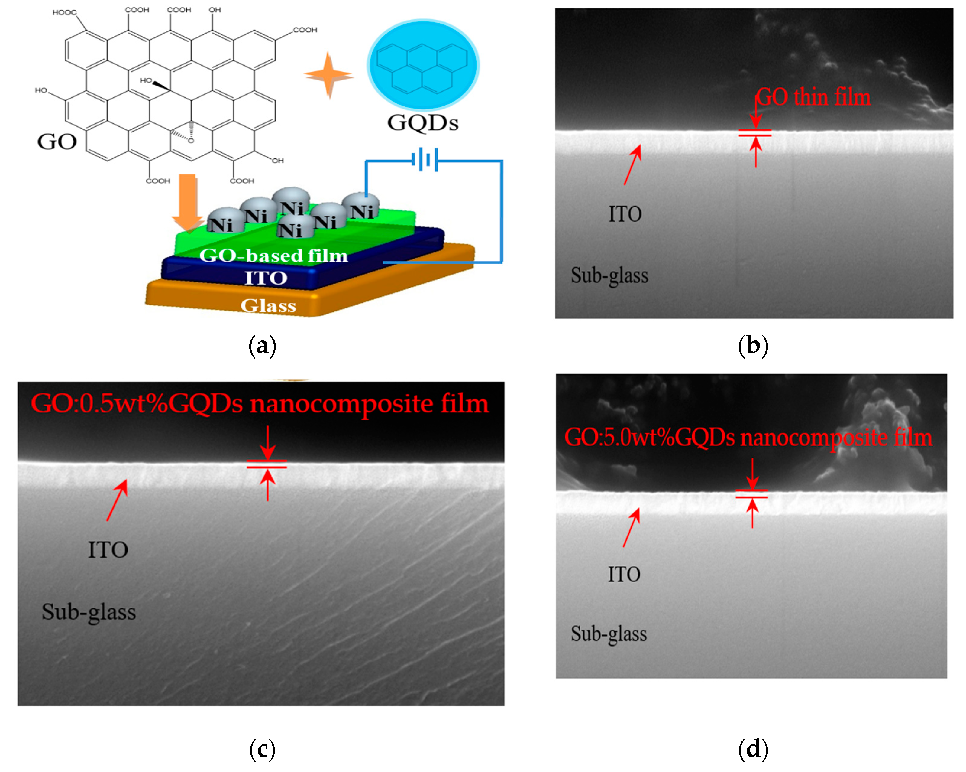
2.1. Preparation of GO:GQDs Memory Devices

The GO powder and GQDs aqueous dispersion were purchased from Tanfeng Tech. Inc. (Suzhou, China) and utilized without further purification. The thickness, diameter and number of GO layers separately ranged from 3.4 nm to 7 nm, from 10 μm to 50 μm, and from 6 to 10. Moreover, the specific area ranged from 100 m2/g to 300 m2/g. Pristine GQDs aqueous solution has a concentration of 1 mg/mL. The thickness, diameter and purity of GQDs is 15 nm, 0.5 nm to 2.0 nm, and ~80% (with a small amount of NaOH to regulate the pH value of the solution), respectively. Both GO and GO:GQDs nanocomposite films, fabricated as below, played the role of the memory layer. They were first prepared by dissolving 50 mg of GO powder in 10 mL of distilled water. The GO solution (5 mg/mL) was stirred overnight to guarantee that it dissolved well. Next, an appropriate amount of the pristine GQDs aqueous solution was added into the dissolved GO solution to generate GO:GQDs nanocomposites with content of GQDs 0.5 wt%, 2.5 wt%, and 5.0 wt% before the prepared GO:GQDs nanocomposite solution was stirred for another 5 h to ensure the homogeneous solution. The glass substrate coated with ITO was ultrasonically washed by being rinsed in acetone, methyl alcohol, and absolute ethyl alcohol, respectively. Then GO and its nanocomposites were blended with different content of GQDs in deionized water, which was separately spin-coated on ITO at 6000 rpm for 60 s and then dried at 100 °C for 2 h to allow any excess solvent to evaporate. Finally, the top Ni electrode was deposited on the top of the memory layer to form a metal-insulator-metal (MIM) structure with an active area of 1 × 1 mm2. Ni electrodes were deposited onto films (coated on the substrates) by ZZ-450A Vacuum Thermal Evaporator (Beiyi Innovation Vaccum Technology; Beijing, China) at a pressure approaching 10−5 Torr.

2.2. Characterization

Different characterization techniques were used to confirm the formation of GO:GQDs nanocomposites in conjunction with nanocomposite film characterization. FTIR spectroscopy (Foss DS 2500 Infrared Spectrometer; Hillerød, Denmark), swept from 400 cm−1 to 4000 cm−1, was recorded. Additionally, Raman spectroscopy (inVia-Reflex; Renishaw, England) was employed to achieve the structure information of GO and GO:GQDs nanocomposites, scanned from 100 cm−1 to 3200 cm−1, with the 532 nm laser-source and the power of the laser 50 mW. Through thermogravimetric analysis and derivative thermogravimetry (TGA-DTG) (TA Instruments; New Castle, DE, USA) analysis, the thermal stability of GO and its nanocomposites was conducted under N2 atmosphere from room temperature growing up to 400 °C at a heating rate of 10 °C/min. Scanning electron microscopy (SEM) (Themoscientific; Waltham, MA, USA) images were obtained at 20 kV and detected under the condition of magnification of 100,000 and working distance (WD) of 10.6 mm, dwell of 5 μs and spot of 10, and PW of 2.7 nm. Transmission electron microscopy (TEM) and high-resolution (HR)-TEM images for GO were characterized by a JEM-2100 TEM (JOEL; Tokyo, Japan) operated at 200 kV. The electrical measurements of ITO/GO/Ni and ITO/GO:GQDs/Ni were fulfilled by a semiconductor parameter analyzer (Keithley 4200; Solon, OH, USA). At room temperature, all electrical experiments were conducted without any device encapsulation in the air.

3. Results and Discussions

3.1. FTIR Analysis

To gain insight into the chemical structures for GO and GO:GQDs nanocomposites, FTIR spectroscopy was used to verify functional group existence (Figure 1) [34]. The peak at 3185 cm-1 was indicated by hydroxyl group (O–H), stretching vibrations of GO when prominent peaks for epoxy (C–O–C) and carboxyl groups (–COOH) were observed at 955 cm−1 to 1100 cm−1, and 1500 cm−1 to 1800 cm−1. The absorption bands at 1725 cm−1, 1163 cm−1 and 1338 cm−1 were attributed to the stretching of the C=O, deformation of OH and stretching of C–O bonds of COOH groups. The stretching of C–O bond, relevant to the epoxide groups, could be seen at 1046 cm−1 when the absorption of C–H stretching could be seen at 2860 cm−1. It was found that there was a series of characteristic absorption peaks in the spectra of GO:GQDs nanocomposites. The peaks (Table 1) were associated with the C–O–C, C–OH, C–C, C=O, and OH groups. In the GO:GQDs nanocomposites, a broad and intense hydroxyl (O–H) peak was responsible for the peak at 3208 cm−1, 3225 cm−1 and 3240 cm−1, respectively. The strong C=O peak at around 1710 cm−1 was a result of stretching vibrations of carboxylic acid and carbonyl moieties, which decreased with the incremental content of GQDs. These clearly indicated that through COO bonding, GQDs were well attached to the GO surface [35]. The FTIR observation confirmed the production of GO:GQDs nanocomposite formation.

3.2. Raman Spectroscopy

Raman spectroscopy was employed to structurally characterize GO and GO:GQDs nanocomposites with 0.5 wt%, 2.5 wt%, and 5.0 wt% GQDs (Figure 2). Two distinct peaks in the spectrum were relative to the broad disorder D-band at 1347 cm−1 and an in-plane vibrational G-band at 1591 cm−1. The D band related to the mode of the k-point photons of A1g symmetry of hybridized carbon atoms accords with sp3 defects, whereas the G band conforms to the E2g phonon of sp2 carbon atoms frequencies, connected with the defect density, disorder, edge structure and smoothness [36]. For GO, the intensity ratio of the D band to G band (ID/IG) was 0.92, which signified that GO was graphitized at low levels on account of oxygen-containing functional groups [37]. It proved the existence of structural defects and disorder in the sp2 network of GO. The estimated intensity ratio of the D band to G band ID/IG for GO:0.5 wt%GQDs nanocomposite was 0.90 while that for GO:5.0wt%GQDs nanocomposite was 0.96, which made clear that GO:5.0 wt%GQDs nanocomposite had more defects and disorders. The broad 2D peak at 2703 cm−1 manifested that the GO sample had a small number of layers [38]. Three low-intensity peaks located at approximately 456 cm−1, 515 cm−1, and 633 cm−1, were observed in GO:GQDs nanocomposites and they could be exclusively attributed to the Eg, F2g and A1g modes of GQDs. Raman spectroscopy gains insight into the ordered and disordered crystal structures of carbon materials. Figure 2b shows the Raman spectrum of the GQDs aqueous dispersion. It indicated a G band at 1643 cm−1, which was a common signature of the first-order scattering of E2g phonon from sp2 carbon graphitic lattice. The D band was very weak, indicating that the arrangement of the GQD layer was orderly.

3.3. Thermal Properties

The thermal stability of GO and GO:GQDs nanocomposites were investigated by TGA in N2 atmosphere (Figure 3). GO was thermally unstable and started to lose mass upon heating below 100 °C because of the adsorbed water molecules. There were two significant steps in mass around the range from 165 °C to 200 °C, which were assigned to the elimination of oxygenated functional groups of GO. A weak mass loss in the range of 250–400 °C was related to the elimination of more stable functional groups. The residual weight of about 8% was obtained, exhibiting that most of GO was burned into volatile gases. Compared with GO, the GO:GQDs nanocomposites showed lower weight loss at the three stages. This was attributed to the presence of more stable oxide groups on the GO:GQDs nanocomposite surface than GO [35]. The remaining weight at 400 °C was about 4%, 30%, and 59% for GO:0.5 wt%GQDs, GO:2.5 wt%GQDs and GO:5.0 wt%GQDs nanocomposites, respectively. The addition of 0.5 wt% GQDs adversely affected the thermal stability of GO when it might be derived from the interaction between GO and GQDs.

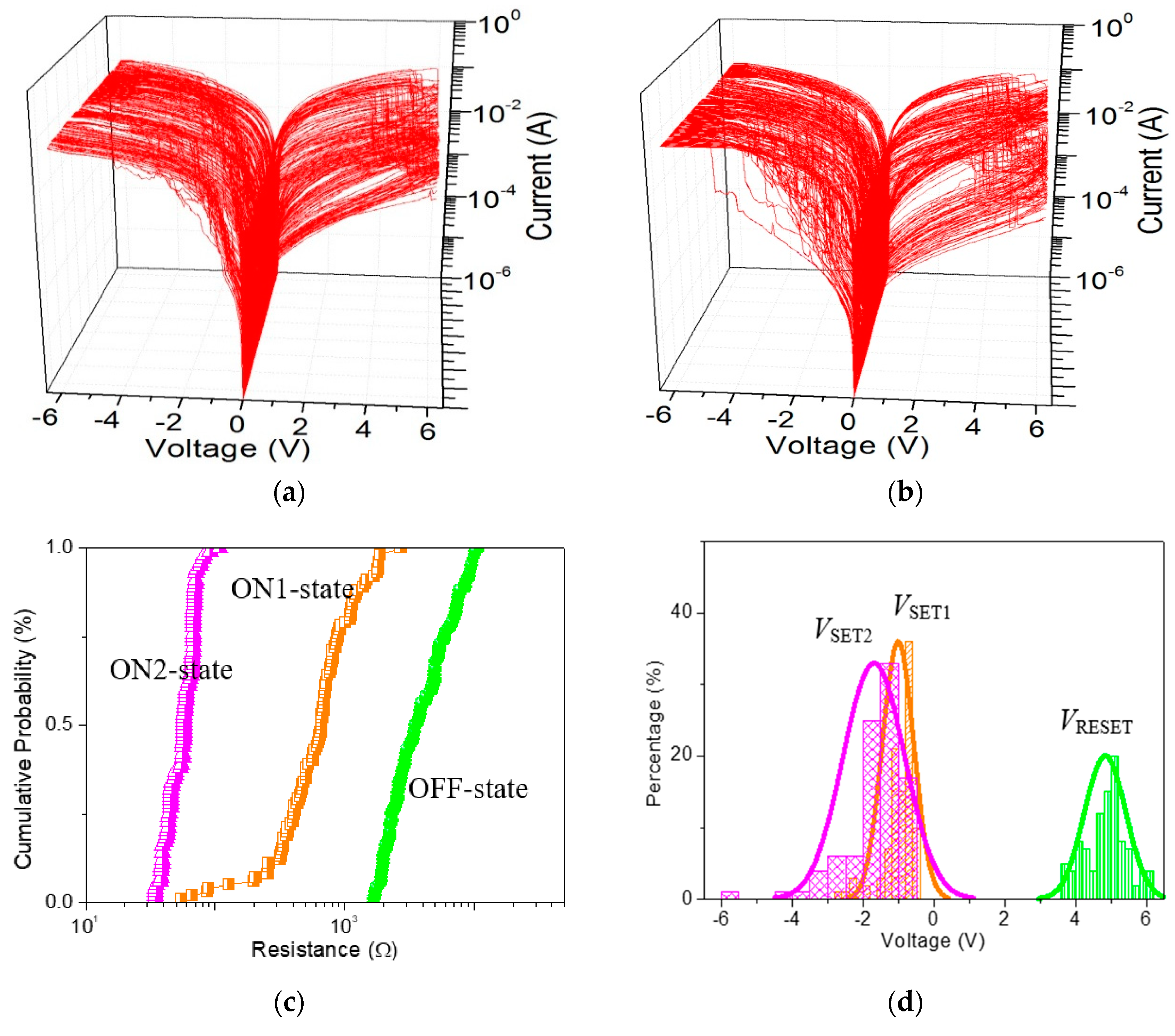
3.4. Memory Characteristics of ITO/GO:GQDs/Ni

A metal/insulator/metal configuration ITO/GO-based film/Ni of memory devices, together with the chemical structures of GO and GQDs can be observed in Figure 4a, which was sandwiched between ITO and Ni electrodes. The cross-sectional profiles of GO and GO:GQDs nanocomposite films were studied by SEM (Figure 4b–d). TEM and HR-TEM images of GO made by magnetically stirring on Cu grids can be observed in Figure 5a,b.
To study the memristic switching effect of GO-based films, the current-voltage (I-V) characteristics of ITO/GO-based film/Ni were tested by direct current DC voltage sweep. During the test, the bias was applied to Ni while ITO was grounded. An ITO/GO:GQDs/Ni memory device with GQDs concentration of 0.5 wt% was fabricated to analyze its behaviors. Two obvious high current jumps arose at −0.9 V (VSET1) and −1.7 V (VSET2) for the tristable memristic switching behaviors (Figure 6a) when the negative voltage was swept from 0 V to −6 V (sweep 1). Three different resistance levels with a current ratio of about 103:102:1 were obtained, regarded as three storage states: “0” (OFF-state or high resistive state (HRS)), “1” (ON1-state or intermediate resistive state (IRS)) and “2” (ON2-state or low resistive state (LRS)). Once the device was written to be the “2” state, positive sweeping (VRESET = 5.14 V) could recover it to the initial “0” state (sweep 3). To demonstrate the nonvolatile nature of the ternary data storage, a small bias voltage (−0.1 V) was used to read the “0”, “1” and “2” states for 104 seconds (Figure 7a) that were kept stable without obvious degradation.
In order to give an insight into the conduction mechanism of the tristable memristic switching based on GO: 0.5 wt%GQDs nanocomposite, memristic switching characteristics of ITO/GO/Ni were implemented under a compliance current (ICC) of 100 mA (Figure 6b). Initially, it recorded that the current gradually increased on the condition of the incremental voltage from 0 V to −2.2 V. However, an abrupt growth in current at the SET voltage (VSET) of −2.25 V contributed to the translation of the device from OFF-state to ON-state. The device was stably preserved in ON-state during the subsequent negative voltage sweep. Next, it was switched from ON-state to OFF-state with positive RESET voltage (VRESET = 4.15 V). For this binary memory device, OFF-state remained intact against positive sweep up to 6 V. Counting on its bistable memristic switching, the resistance ratio of the device between OFF-state and ON-state was above 102. The OFF-state and ON-state retention of the ITO/GO/Ni memory device without embedded GQDs (Figure 7b) exhibited the device could not be switched between ON-state and OFF-state by applying a constant reading bias of −0.1 V. Taking the bistable memristic switching of GO into consideration, the ternary memory of GO:GQDs nanocomposite was associated with GQDs.
As for ITO/GO:0.5 wt%GQDs/Ni (Figure 8a), the cumulative plots of the resistance in OFF-state, ON1-state, and ON2-state (ROFF, RON1, and RON2), as well as histograms of VSET1, VSET2 and VRESET, demonstrate the data distributions during the cycle-to-cycle (C/C) operation (Figure 8b,c). The mean values (standard deviation) μ(σ) of VSET1, VSET2 and VRESET were −1.12(0.37) V, −1.88(0.69) V and 4.14(0.77) V, respectively, while that of ROFF, RON1, and RON2 were 84.6(13.3) kΩ, 5.4(7.1) kΩ, and 48.9(11.9) Ω, respectively. For device analyses of the device-to-device (D/D) operation (Figure 8d), μ(σ) for ROFF, RON1, and RON2 was 36.0(34.6) kΩ, 7.5(7.8) kΩ, and 52.5(12.6) Ω, respectively. The binary memory performance of GO (Figure 9a) was meticulously studied. The cumulative plots of the resistance in OFF and ON states (ROFF and RON), as well as histograms of VSET and VRESET, demonstrated the data distributions of ITO/GO/Ni during the C/C operation (Figure 9b,c). The μ and σ of VSET were −0.95 V and 0.45 V when that of VRESET was 4.56 V and 0.57 V. The small values of σ could be related to less spread in the distribution of VSET and VRESET. Device uniformity for ROFF and RON during the D/D performance (Figure 9d) indicated the value μ(σ) of ROFF and RON was 3.2(1.6) kΩ and 53.8(12.1) Ω, 4.5(5.4) kΩ and 72.6(21.9) Ω for C/C and D/D operations, respectively. By doping GQDs into GO, the memory performance tunable from binary to ternary was observed to assess the possible application of the GO-based nanocomposite in all-inorganic, multi-bit resistive random-access memory (RRAM).
To better understand the impact of GQDs on the tristable memristic switching behaviors, ITO/GO:GQDs/Ni devices with various GQDs concentrations (0.5 wt%, 2.5 wt% and 5.0 wt%) were fabricated and compared (Figure 10). Furthermore, ternary memory characteristics with the proportion ROFF/RON1/RON2 approaching 102:10:1 were achieved by recording 100 consecutive sweeping cycles for Ni/GO:2.5 wt%GQDs/ITO and Ni/GO: 5.0 wt%GQDs/ITO. The main role of these GQDs in tristable memristic switching has to be investigated in depth. In contrast with ITO/GO: 0.5 wt%GQDs/Ni, the tristable memristic switching transition among HRS, IRS and LRS could be obviously observed under ICC of 0.1 A when the memory cells were detected under 100 switching cycles. It could be observed with negative voltage sweeping, indicating the potential of multi-bit data storage. However, there is a significant overlap between VSET1 and VSET2, which needs to be settled in the future. The coefficient of variation (σ/μ) of ROFF, RON1 and VRESET reduced with incremental content of GQDs for the ITO/GO:GQDs/Ni memory cell, estimated in Table 2 and Table 3. Ternary memory behaviors with different content of GQDs (0.5 wt%, 2.5 wt% and 5.0 wt%) in the device Ni/GO:GQDs/ITO recorded that I-V curves with successive cycles were greatly stabilized by inserting GQDs into the GO layer. To summarize, all the above-mentioned results experimentally demonstrated that improved IRS and HRS robustness can be obtained by embedding GQDs in GO-based RRAM. Thus, such devices exhibit the feasibility of multi-bit RRAM.

3.5. Conduction Mechanism of ITO/GO-Based Film/Ni

Figure 11 illustrates a log-log plot of I-V curves on the basis of ITO/GO-based film/Ni with and without embedded GQDs. The LRS of both devices showed similar Ohmic behavior, with logI-logV slope of ~1, while HRS showed a dependence on the GQDs concentration (Table 2). For the device ITO/GO/Ni, the HRS conduction can be divided into three regions: Ohmic conduction in the low voltage region and almost linear conduction in the high voltage region with a slope of ~2 and ~4, which can be approximately linked to Ohm’s law and trap filled-limited (TFL) behavior (IVn) in a space charge-limited conduction model (SCLC). Herein, the injected charge carriers were believed to be captured in GO up to saturation. As the positive voltage increased, the high voltage in GO layer brought about electron detrapping. The small slope (~2) of TFL behavior in ITO/GO:0.5 wt%GQDs/Ni may be related to the shallow trapping level in the GO film. Interestingly, the slope of TFL behavior increased and saturated (a slope of ~3 in IRS of the tristable memristic switching) for the devices with embedded GQDs. It was consistent with trap-filling, which means trapping centers with deeper levels were induced by GQDs. In the low bias voltage region, the current followed Ohmic conduction (IV) because of the thermal excitation of the filled traps. With the bias growing, the traps were gradually filled. I-V curves approximately obeyed a square law (IV2), called by trap-filled limited current mode (TFLC). When the voltage further increased to the first threshold voltage, all traps in GO were filled up, and the conductivity of the film rapidly jumped to a higher level (“1” state). Approximately, the current was designated as space charge limited current (SCLC) region. When the voltage overcame the second threshold voltage, all traps in GO:GQDs films associated with GQDs held a stable line and the conductivity of the film rapidly jumped to a higher level (“2” state, IV3). The aforementioned conclusions were further corroborated upon application of both Poole–Frenkel and Schottky emission mechanisms to fit the conduction performance. The plots of log(I/V)-V1/2 and lnI-V1/2 before transition to Ohmic conduction were not linear and demonstrated a parabolic behavior. In summary, the impact of GQDs embedded in GO-based RRAM devices is an increase in HRS, IRS and VRESET. Since GQDs have similar chemical structures and charge trapping effects, embedding them in GO can strongly impact the electrical properties of pristine GO films and deepen the charge trapping level, which gives rise to multi-bit memristic switching behaviors.

4. Conclusions

In summary, memristic switching behaviors of all-inorganic multi-bit memory devices by means of the simple solution-processable method were tuned from binary to ternary through doping GQDs as charge-trapping centres into GO. An approach to improve the tristable memristic switching behaviors, such as the parameters RIRS and ROFF was demonstrated by the C/C operation. The coefficient of variation (σ/μ) of ROFF, RON1 and VRESET separately reduced to 45.09%, 55.3% and 13.3% with incremental content of GQDs for the ITO/GO:GQDs/Ni memory cell while still maintaining a resistance ratio (ROFF/RON1/RON2) of over 102:10:1. These results provide an approach to significantly decrease memristor switching variability from cycle to cycle.

Funding

This work was supported by Science Foundation Project of Heilongjiang Province of China (No. QC2018084), University Nursing Program for Young Scholars with Creative Talents in Heilongjiang Province (No. UNPYSCT-2018007) and Key Laboratory of Functional Inorganic Material Chemistry (Heilongjiang University), Ministry of Education, China.

Acknowledgments

This work was supported by Science Foundation Project of Heilongjiang Province of China (No. QC2018084), University Nursing Program for Young Scholars with Creative Talents in Heilongjiang Province (No. UNPYSCT-2018007) and Key Laboratory of Functional Inorganic Material Chemistry (Heilongjiang University), Ministry of Education, China.

Conflicts of Interest

The author declares no conflict of interest.

References

  1. Strukov, D.B.; Snider, G.S.; Stewart, D.R.; Williams, R.S. The missing memristor found. Nature 2008, 453, 80–83. [Google Scholar] [CrossRef]
  2. Kim, T.H.; Jang, E.Y.; Lee, N.J.; Choi, D.J.; Lee, K.-J.; Jang, J.-T.; Choi, J.-S.; Moon, S.H.; Cheon, J. Nanoparticle assemblies as memristors. Nano Lett. 2009, 9, 2229–2233. [Google Scholar] [CrossRef]
  3. Abraham, I. The case for injecting the memristor as a fundamental circuit element. Sci. Rep. 2018, 8, 10972–10980. [Google Scholar] [CrossRef]
  4. Vongehr, S.; Meng, X. The missing memristor has not been found. Sci. Rep. 2015, 5, 11657–11663. [Google Scholar] [CrossRef]
  5. Huebner, C.F.; Tsyalkovsky, V.; Bandera, Y.; Burdette, M.K.; Shetzline, J.A.; Tonkin, C.; Creager, S.E.; Foulger, S.H. Nonvolatile optically-erased colloidal memristors. Nanoscale 2015, 7, 1270–1279. [Google Scholar] [CrossRef]
  6. Li, L.; Wen, D. Memristic characteristics from bistable to tristable memory with controllable charge trap carbon nanotubes. Nanomaterials 2018, 8, 114. [Google Scholar] [CrossRef] [PubMed] [Green Version]
  7. Li, L.; Wen, D. Ternary memristic effect of trilayer-structured graphene-based memory devices. Nanomaterials 2019, 9, 518. [Google Scholar] [CrossRef] [Green Version]
  8. Torres-Costa, V.; Mäkilä, E.; Granroth, S.; Kukk, E.; Salonen, J. Synaptic and fast switching memristance in porous silicon-based structures. Nanomaterials 2019, 9, 825. [Google Scholar] [CrossRef] [PubMed] [Green Version]
  9. Jeong, D.S.; Kim, K.M.; Kim, S.; Choi, B.J.; Hwang, C.S. Memristors for energy-efficient new computing paradigms. Adv. Electron. Mater. 2016, 2, 1600090–1600116. [Google Scholar] [CrossRef]
  10. Huang, P.; Kang, J.; Zhao, Y.; Chen, S.; Han, R.; Zhou, Z.; Chen, Z.; Ma, W.; Li, M.; Liu, L.; et al. Reconfigurable nonvolatile logic operations in resistance switching crossbar array for large-scale circuits. Adv. Mater. 2016, 28, 9758–9764. [Google Scholar] [CrossRef] [PubMed]
  11. Duan, W.J.; Wang, J.B.; Zhong, X.L. Electrically-controlled nonlinear switching and multi-level storage characteristics in WOx film-based memory cells. J. Phys. Chem. Solids 2018, 116, 148–152. [Google Scholar] [CrossRef]
  12. Yanga, Y.; Lub, H.; Liub, J.; Shen, Y. Synthesis and binary/ternary write-once read-many-times electrical memory behaviors of carbazole-based polyimides bearing flexible linkage segment. Eur. Polym. J. 2018, 108, 10–19. [Google Scholar] [CrossRef]
  13. Zhao, Y.-Y.; Cheng, X.-F.; Qian, W.H.; Zhou, J.; Sun, W.-J.; Hou, X.; He, J.-H.; Li, H.; Xu, Q.-F.; Li, N.-J.; et al. Mussel-inspired polydopamine coating for flexible ternary resistive memory. Chem. Asian J. 2018, 13, 1744–1750. [Google Scholar] [CrossRef] [PubMed]
  14. Hong, E.Y.-H.; Poon, C.-T.; Yam, V.W.W. A phosphole oxide-containing organogold(III) complex for solution-processable resistive memory devices with ternary memory performances. J. Am. Chem. Soc. 2016, 138, 6368–6371. [Google Scholar] [CrossRef] [Green Version]
  15. Jiang, X.; Lu, G.; Huang, X.; Li, Y.; Cao, F.; Chen, H.; Liu, W. Thermo-responsive graphene oxide/poly(ethyl ethylene phosphate) nanocomposite via ring opening polymerization. Nanomaterials 2019, 9, 207. [Google Scholar] [CrossRef] [Green Version]
  16. Dikin, D.A.; Stankovich, S.; Zimney, E.J.; Piner, R.D.; Dommett, G.H.B.; Evmenenko, G.; Nguyen, S.T.; Ruoff, R.S. Preparation and characterization of graphene oxide paper. Nature 2007, 448, 457–460. [Google Scholar] [CrossRef]
  17. Salesa, B.; Llorens-Gámez, M.; Serrano-Aroca, Á. Study of 1D and 2D carbon nanomaterial in alginate films. Nanomaterials 2020, 10, 206. [Google Scholar] [CrossRef] [Green Version]
  18. Aliyev, E.; Filiz, V.; Khan, M.M.; Lee, Y.J.; Abetz, C.; Abetz, V. Structural characterization of graphene oxide: Surface functional groups and fractionated oxidative debris. Nanomaterials 2019, 9, 1180. [Google Scholar] [CrossRef] [Green Version]
  19. Ahmad, H.; Fan, M.; Hui, D. Graphene oxide incorporated functional materials: A review. Compos. Part B Eng. 2018, 145, 270–280. [Google Scholar] [CrossRef]
  20. Perrozzi, F.; Prezioso, S.; Ottaviano, L. Graphene oxide: From fundamentals to applications. J. Phys. Condens. Matter 2014, 27, 013002. [Google Scholar] [CrossRef] [Green Version]
  21. Yu, X.; Sun, S.; Zhou, L.; Miao, Z.; Zhang, X.; Su, Z.; Wei, G. Removing metal ions from water with graphene–bovine serum albumin hybrid membrane. Nanomaterials 2019, 9, 276. [Google Scholar] [CrossRef] [PubMed] [Green Version]
  22. Hasan, M.T.; Gonzalez-Rodriguez, R.; Ryan, C.; Faerber, N.; Coffer, J.L.; Naumov, A.V. Photo-and electroluminescence from nitrogen-doped and nitrogen-sulfur codoped graphene quantum dots. Adv. Funct. Mater. 2018, 28, 1804337. [Google Scholar] [CrossRef]
  23. Zhang, W.; Gan, J. Synthesis of blue-photoluminescent graphene quantum dots/polystyrenic anion-exchange resin for Fe(III) detection. Appl. Surf. Sci. 2016, 372, 145–151. [Google Scholar] [CrossRef]
  24. Zhao, M.; Yang, F.; Xue, Y.; Xiao, D.; Guo, Y. A time-dependent DFT study of the absorption and fluorescence properties of graphene quantum dots. Chemphyschem 2014, 15, 950–957. [Google Scholar] [CrossRef]
  25. Lin, L.; Rong, M.; Luo, F.; Chen, D.; Wang, Y.; Chen, X. Luminescent graphene quantum dots as new fluorescent materials for environmental and biological applications. TrAC Trends Anal. Chem. 2014, 54, 83–102. [Google Scholar] [CrossRef]
  26. Shen, J.; Zhu, Y.; Yang, X.; Li, C. Graphene quantum dots: Emergent nanolights for bioimaging, sensors, catalysis and photovoltaic devices. Chem. Commun. 2012, 48, 3686–3699. [Google Scholar] [CrossRef]
  27. Hümmelgen, I.A.; Coville, N.J.; Cruz-Cruz, I.; Rodrigues, R. Carbon nanostructures in organic WORM memory devices. J. Mater. Chem. C 2014, 2, 7708–7714. [Google Scholar] [CrossRef] [Green Version]
  28. Chen, Y.; Liu, G.; Wang, C.; Zhang, W.; Li, R.-W.; Wang, L. Polymer memristor for information storage and neuromorphic applications. Mater. Horiz. 2014, 1, 489–506. [Google Scholar] [CrossRef]
  29. Torculas, M.; Medina, J.; Xue, W.; Hu, X. Protein-based bioelectronics. ACS Biomater. Sci. Eng. 2016, 2, 1211–1223. [Google Scholar] [CrossRef]
  30. Wang, W.; Xu, J.; Ma, H.; Zhao, X.; Lin, Y.; Zhang, C.; Wang, Z.; Xu, H.; Liu, Y. Insertion of nanoscale AgInSbTe layer between the Ag electrode and the CH3NH3PbI3 electrolyte layer enabling enhanced multilevel memory. ACS Appl. Nano Mater. 2019, 2, 307–314. [Google Scholar] [CrossRef]
  31. Yin, Y.; Zeng, F.; Wan, Q.; Li, F.; Sun, Y.; Hu, Y.; Liu, J.; Li, G.; Pan, F. Adaptive crystallite kinetics in homogenous bilayer oxide memristor for emulating diverse synaptic plasticity. Adv. Funct. Mater. 2018, 28, 1706927–1706936. [Google Scholar] [CrossRef]
  32. Spassov, D.; Paskaleva, A.; Krajewski, T.A.; Guziewicz, E.; Luka, G.; Ivanov, T. Al2O3/HfO2 multilayer high-k dielectric stacks for charge trapping flash memories. Phys. Status Solidi A 2018, 215, 1700854–1700861. [Google Scholar] [CrossRef]
  33. Jung, J.; Kwon, D.; Jung, H.; Lee, K.; Yoon, T.-S.; Kang, C.J.; Lee, H.H. Multistate resistive switching characteristics of ZnO nanoparticles embedded polyvinylphenol device. J. Ind. Eng. Chem. 2018, 64, 85–89. [Google Scholar] [CrossRef]
  34. Olad, A.; Hagh, H.B.K. Graphene oxide and amin-modified graphene oxide incorporated chitosan gelatin scaffolds as promising materials for tissue engineering. Compos. Part B 2019, 162, 692–702. [Google Scholar] [CrossRef]
  35. Karimi, B.; Ramezanzadeh, B. A comparative study on the effects of ultrathin luminescent graphene oxide quantum dot (GOQD) and graphene oxide (GO) nanosheets on the interfacial interactions and mechanical properties of an epoxy composite. J. Colloid Interface Sci. 2017, 493, 62–76. [Google Scholar] [CrossRef]
  36. Alves, A.K.; Frantz, A.C.S.; Berutti, F.A. Microwave-assisted oleothermal synthesis of graphene-TiO2 quantum dots for photoelectrochemical oxygen evolution reaction. FlatChem 2018, 12, 26–34. [Google Scholar] [CrossRef]
  37. Riaz, R.; Ali, M.; Anwer, H.; Ko, M.J.; Jeong, S.H. Highly porous self-assembly of nitrogen-doped graphene quantum dots over reduced graphene sheets for photo-electrocatalytic electrode. J. Colloid Interface Sci. 2019, 557, 174–184. [Google Scholar] [CrossRef]
  38. Park, J.S.; Reina, A.; Saito, R.; Kong, J.; Dresselhaus, G.; Dresselhaus, M.S. G’ band Raman spectra of single, double and triple layer graphene. Carbon 2009, 47, 1303–1310. [Google Scholar] [CrossRef]
Figure 1. FTIR spectra of GO, and GO:GQDs nanocomposites.
Nanomaterials 10 01448 g001
Figure 2. (a) Raman spectra of GO and its nanocomposites with different content of GQDs 0.5 wt%, 2.5 wt%, and 5.0 wt%, respectively; (b) Raman spectrum of GQDs aqueous dispersion.
Nanomaterials 10 01448 g002
Figure 3. (a) Thermogravimetric analysis (TGA) and (b) derivative thermogravimetry (DTG) of GO as well as its nanocomposites.
Nanomaterials 10 01448 g003
Figure 4. (a) Sandwiched scheme of ITO/GO-based/Ni together with structure of chemical component GO and GQDs; (bd) SEM images for the cross-sectional characterization of GO, GO:0.5 wt%GQDs, and GO:5.0 wt%GQDs nanocomposite thin films spin-coated onto ITO/glass substrates, respectively.
Nanomaterials 10 01448 g004
Figure 5. (a) Transmission electron microscopy (TEM) and (b) high-resolution (HR-TEM images of GO made by magnetically stirring.
Nanomaterials 10 01448 g005
Figure 6. Memristic switching characteristics for (a) ITO/GO:0.5 wt%GQDs/Ni and (b) ITO/GO/Ni.
Nanomaterials 10 01448 g006
Figure 7. Retention property of (a) ITO/GO:0.5 wt%GQDs/Ni device and (b) ITO/GO/Ni. The resistance value was read at a constant voltage of −0.1 V.
Nanomaterials 10 01448 g007
Figure 8. (a) 100 tristable sweeping cycles for ITO/GO:0.5 wt%GQDs/Ni; (b) Cumulative probability of the resistance in OFF, ON1 and ON2 states (ROFF, RON1 and RON2), and (c) histograms of the SET1, SET2 and RESET voltage (VSET1, VSET2 and VRESET) with respect to cycle-to-cycle operation in ITO/GO:0.5 wt%GQDs/Ni; (d) Device uniformity for 20 ITO/GO:0.5 wt%GQDs/Ni cells concerning ROFF, RON1 and RON2.
Nanomaterials 10 01448 g008
Figure 9. (a) 100 bistable switching cycles of ITO/GO/Ni; (b) Cumulative probability for the resistance of the device in OFF-state and ON-state (ROFF and RON), and (c) the SET and RESET voltage (VSET and VRESET) with respect to cycle-to-cycle operation in ITO/GO/Ni; (d) Device-to-device uniformity for 20 device cells concerning ROFF and RON.
Nanomaterials 10 01448 g009
Figure 10. Cycle-to-cycle operation for (a,b) ITO/GO:2.5 wt%GQDs/Ni and ITO/GO:5.0 wt%GQDs/Ni; (c,d) Resistance distribution (ROFF, RON1 and RON2) in probability, and (e,f) VSET, VSET2 and VRESET distributions in histogram for the cycle-to-cycle process.
Nanomaterials 10 01448 g010aNanomaterials 10 01448 g010b
Figure 11. Double-logarithmic plots for (a,b) set and (c,d) reset process with the space-charge-limited model fitting for ITO /GO/ Ni and ITO /GO:0.5 wt%GQDs/ Ni, respectively.
Nanomaterials 10 01448 g011
Table 1. Data for FTIR spectroscopy of GO and GO:GQDs nanocomposites.
υC-O-C (cm−1)υC-OH (cm−1)υC-C (cm−1)υC=O (cm−1)υOH (cm−1)
GO10461338162217203185
GO:0.5 wt%GQDs10421359162217143208
GO:2.5 wt%GQDs10521377157217113225
GO:5.0 wt%GQDs10691383156916963240
Table 2. Data analyses for GO:GQDs nanocomposites concerning the mean value (μ) and standard deviation (σ) of the resistance in OFF, ON1, and ON2 states (ROFF, RON1, and RON2).
ROFF (Ω)RON1 (Ω)RON2 (Ω)
μσμ/σμσμ/σμσμ/σ
GO:0.5 wt%GQDs8.5 × 1041.3 × 105157.7%5.4 × 1037.1 × 103131.3%48.911.924.4%
GO:2.5 wt%GQDs4.5 × 1032.6 × 10356.4%760.3516.768.0%56.914.024.7%
GO:5.0 wt%GQDs4.8 × 1032.2 × 10345.9%687.9380.355.3%64.219.830.9%
Table 3. Values μ and σ of the SET1, SET2 and RESET voltages (VSET1, VSET2, and VRESET) based on ternary memory performance.
VSET1 (V)VSET2 (V)VRESET (V)
μσμ/σμσμ/σμσμ/σ
GO:0.5 wt%GQDs−1.120.3733.4%−1.880.6936.8%4.140.7718.5%
GO:2.5 wt%GQDs−1.000.4444.2%−1.690.8751.4%4.840.5912.9%
GO:5.0 wt%GQDs−0.960.5253.5%−1.850.9350.5%4.640.6213.3%

