
Comparison of Sb2O3 and Sb2O3/SiO2 Double Stacked pH Sensing Membrane Applied in Electrolyte-Insulator-Semiconductor Structure

 , and
, and 
Abstract
:1. Introduction
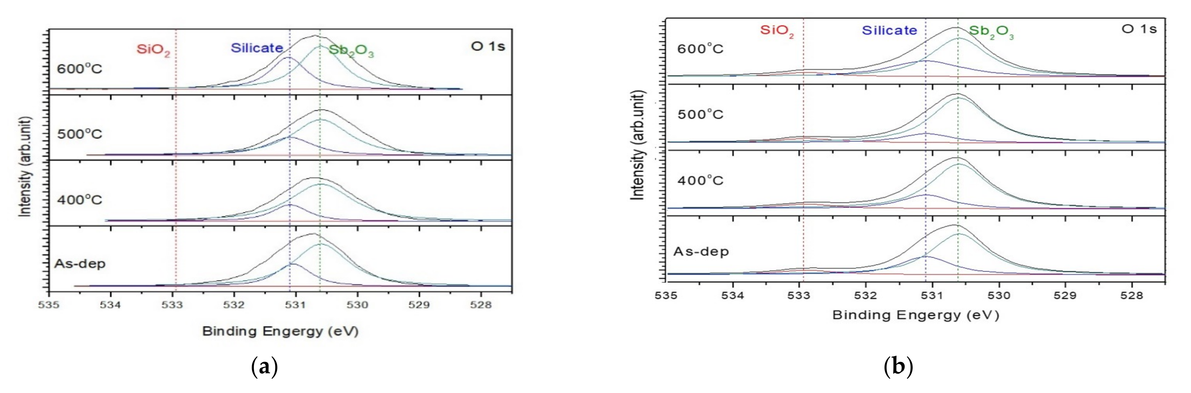
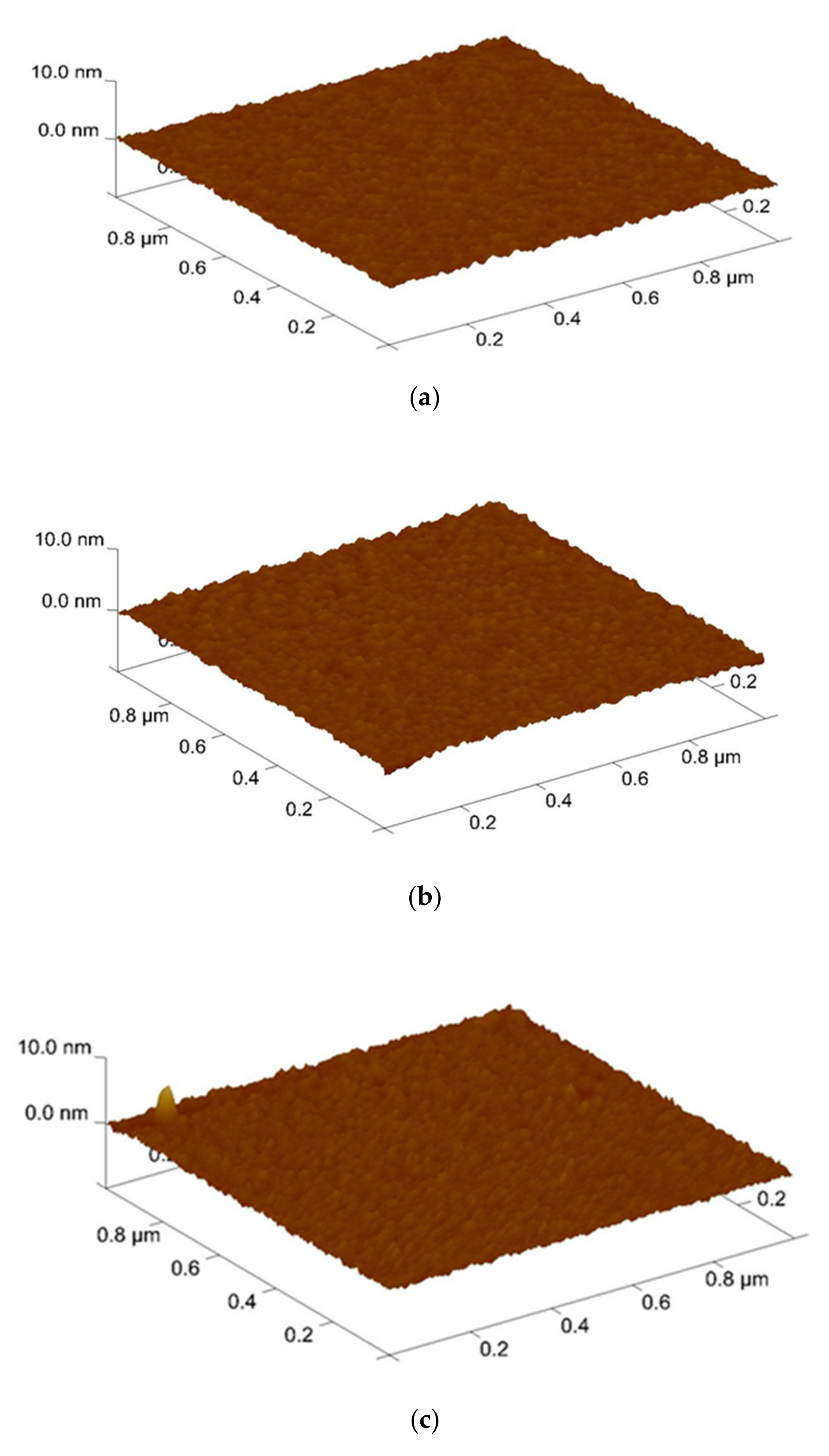
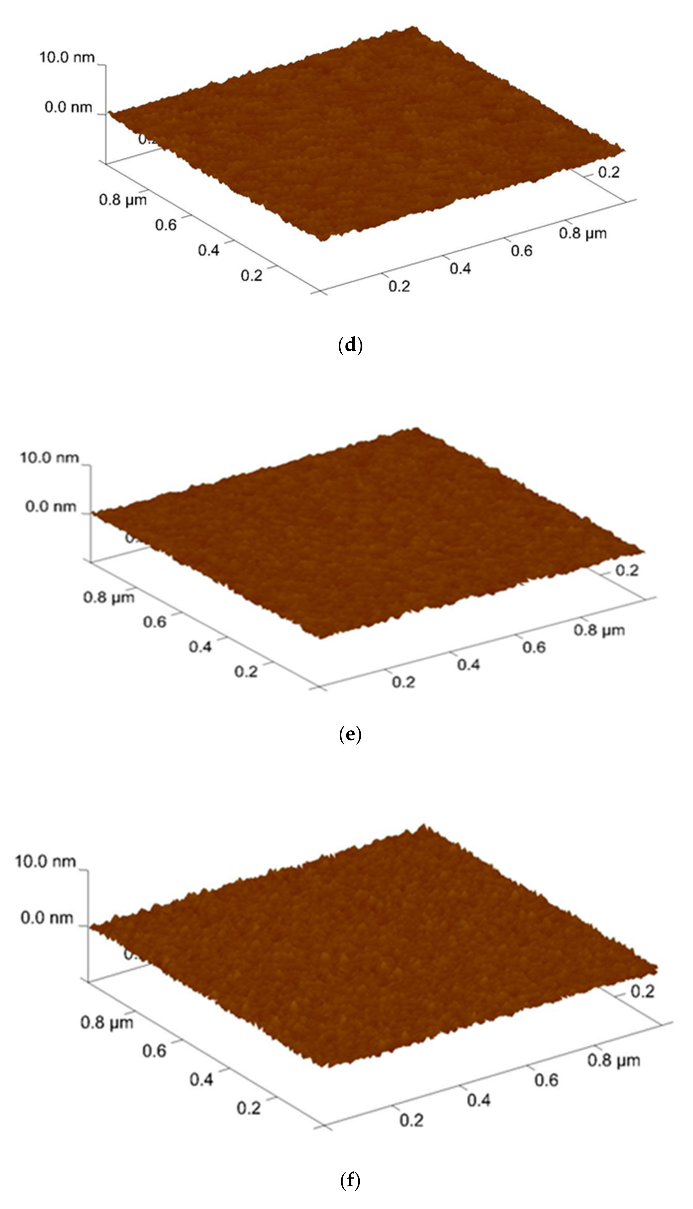
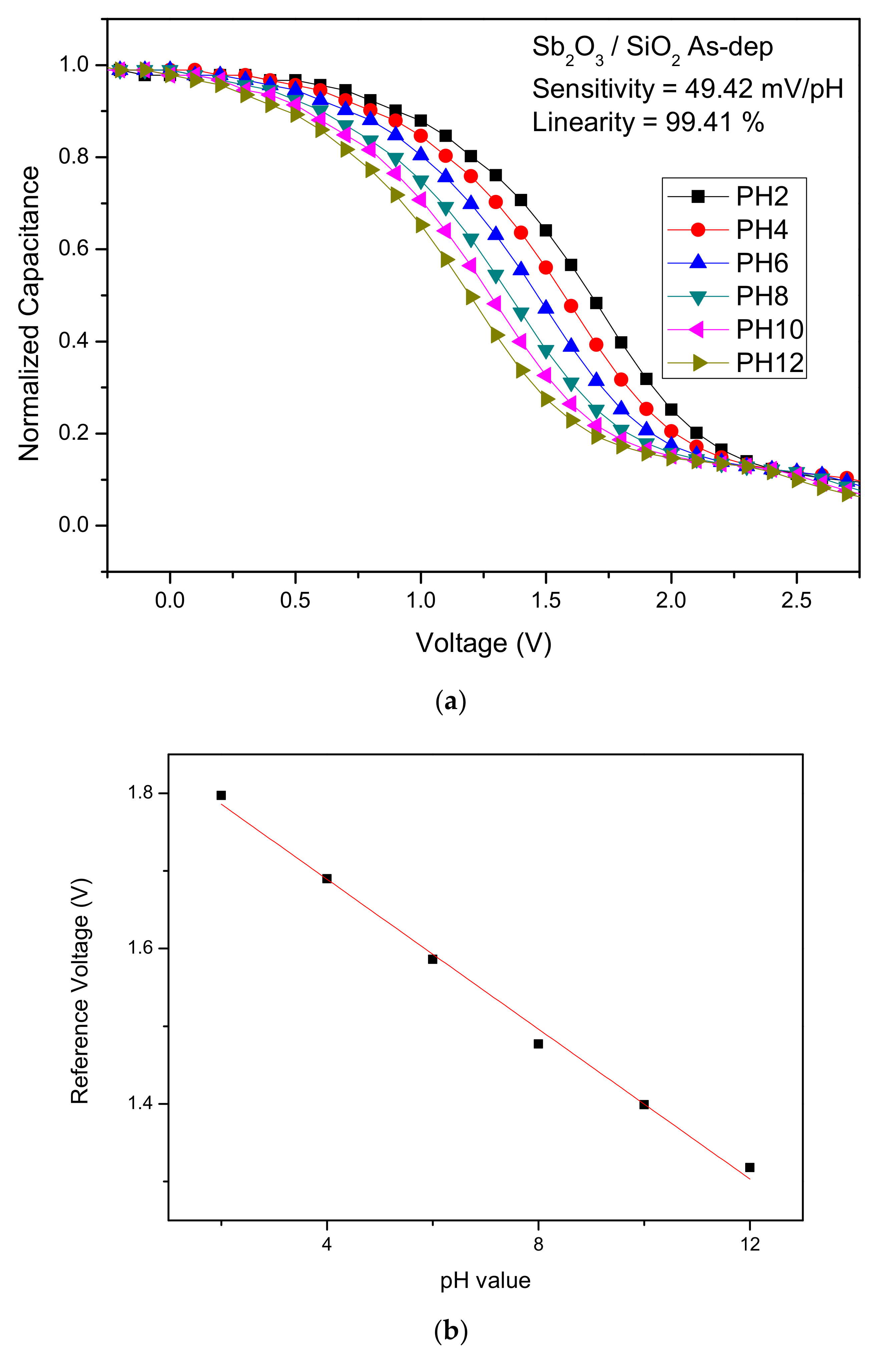
2. Experimental
3. Conclusions
Author Contributions
Funding
Data Availability Statement
Acknowledgments
Conflicts of Interest
References
- Song, Z.; Fan, G.-C.; Li, Z.; Gao, F.; Luo, X. Universal design of selectivity-enhanced photoelectrochemical enzyme sensor: Integrating photoanode with biocathode. Anal. Chem. 2018, 90, 10681–10687. [Google Scholar] [CrossRef] [PubMed]
- Streeck, H.; Schulte, B.; Kümmerer, B.M.; Richter, E.; Höller, T.; Fuhrmann, C.; Bartok, E.; Dolscheid-Pommerich, R.; Berger, M.; Wessendorf, L. Infection fatality rate of SARS-CoV2 in a super-spreading event in Germany. Nat. Commun. 2020, 11, 5829. [Google Scholar] [CrossRef] [PubMed]
- Hattori, Y.; Taniguchi, T.; Watanabe, K.; Nagashio, K. Layer-by-layer dielectric breakdown of hexagonal boron nitride. ACS Nano 2015, 9, 916–921. [Google Scholar] [CrossRef] [Green Version]
- Zhang, B.; Liu, Y. A review of GaN-based optoelectronic devices on silicon substrate. Chin. Sci. Bull. 2014, 59, 1251–1275. [Google Scholar] [CrossRef]
- Prakash, S.; Kalaignan, G.P. Investigation of morphological changes on nickel manganese oxide and their capacitance activity. Colloids Surf. A Physicochem. Eng. Asp. 2021, 611, 125875. [Google Scholar] [CrossRef]
- Nie, J.; Ren, Z.; Xu, L.; Lin, S.; Zhan, F.; Chen, X.; Wang, Z.L. Probing contact-electrification-induced electron and ion transfers at a liquid–solid interface. Adv. Mater. 2020, 32, 1905696. [Google Scholar] [CrossRef]
- Hankin, A.; Bedoya-Lora, F.E.; Alexander, J.C.; Regoutz, A.; Kelsall, G.H. Flat band potential determination: Avoiding the pitfalls. J. Mater. Chem. A 2019, 7, 26162–26176. [Google Scholar] [CrossRef] [Green Version]
- Ko, B.-S.; Lee, G.-Y.; Choi, K.-Y.; Kim, R.-Y. A coordinated droop control method using a virtual voltage axis for power management and voltage restoration of dc microgrids. IEEE Trans. Ind. Electron. 2018, 66, 9076–9085. [Google Scholar] [CrossRef]
- Lee, S.-M.; Han, N.; Lee, R.; Choi, I.-H.; Park, Y.-B.; Shin, J.-S.; Yoo, K.-H. Real-time monitoring of 3D cell culture using a 3D capacitance biosensor. Biosens. Bioelectron. 2016, 77, 56–61. [Google Scholar] [CrossRef] [PubMed]
- Chen, K.-H.; Wood, K.N.; Kazyak, E.; LePage, W.S.; Davis, A.L.; Sanchez, A.J.; Dasgupta, N.P. Dead lithium: Mass transport effects on voltage, capacity, and failure of lithium metal anodes. J. Mater. Chem. A 2017, 5, 11671–11681. [Google Scholar] [CrossRef]
- Huang, Y.; Guo, Z.; Liu, H.; Zhang, S.; Wang, P.; Lu, J.; Tong, Y. Heterojunction architecture of N-doped WO3 nanobundles with Ce2S3 nanodots hybridized on a carbon textile enables a highly efficient flexible photocatalyst. Adv. Funct. Mater. 2019, 29, 1903490. [Google Scholar] [CrossRef]
- Italiano, C.; Llorca, J.; Pino, L.; Ferraro, M.; Antonucci, V.; Vita, A. CO and CO2 methanation over Ni catalysts supported on CeO2, Al2O3 and Y2O3 oxides. Appl. Catal. B Environ. 2020, 264, 118494. [Google Scholar] [CrossRef]
- Siakavelas, G.I.; Charisiou, N.D.; AlKhoori, S.; AlKhoori, A.A.; Sebastian, V.; Hinder, S.J.; Baker, M.A.; Yentekakis, I.; Polychronopoulou, K.; Goula, M.A. Highly selective and stable nickel catalysts supported on ceria promoted with Sm2O3, Pr2O3 and MgO for the CO2 methanation reaction. Appl. Catal. B Environ. 2021, 282, 119562. [Google Scholar] [CrossRef]
- Tian, X.; Shibayama, S.; Nishimura, T.; Yajima, T.; Migita, S.; Toriumi, A. Evolution of ferroelectric HfO2 in ultrathin region down to 3 nm. Appl. Phys. Lett. 2018, 112, 102902. [Google Scholar] [CrossRef]
- Pacchioni, G.; Skuja, L.; Griscom, D.L. Defects in SiO2 and Related Dielectrics: Science and Technology; Springer Science & Business Media: Berlin/Heidelberg, Germany, 2012; Volume 2. [Google Scholar]
- Spinelle, L.; Gerboles, M.; Kok, G.; Persijn, S.; Sauerwald, T. Review of portable and low-cost sensors for the ambient air monitoring of benzene and other volatile organic compounds. Sensors 2017, 17, 1520. [Google Scholar] [CrossRef] [PubMed] [Green Version]
- Xing, P.; Ma, D.; Ooi, K.J.; Choi, J.W.; Agarwal, A.M.; Tan, D. CMOS-compatible PECVD silicon carbide platform for linear and nonlinear optics. ACS Photonics 2019, 6, 1162–1167. [Google Scholar] [CrossRef]
- Jiang, X.; Ma, Z.; Xu, J.; Chen, K.; Xu, L.; Li, W.; Huang, X.; Feng, D. a-SiN x: H-based ultra-low power resistive random access memory with tunable Si dangling bond conduction paths. Sci. Rep. 2015, 5, 15762. [Google Scholar] [CrossRef] [Green Version]
- Xie, L.-Q.; Chen, L.; Nan, Z.-A.; Lin, H.-X.; Wang, T.; Zhan, D.-P.; Yan, J.-W.; Mao, B.-W.; Tian, Z.-Q. Understanding the cubic phase stabilization and crystallization kinetics in mixed cations and halides perovskite single crystals. J. Am. Chem. Soc. 2017, 139, 3320–3323. [Google Scholar] [CrossRef]
- Abass, K.H.; Obaid, N.H. 0.006 wt.% Ag-Doped Sb2O3 Nanofilms with Various Thickness: Morphological and optical properties. J. Phys. Conf. Ser. 2019, 1294, 022005. [Google Scholar] [CrossRef]
- Lin, C.F.; Kao, C.H.; Lin, C.Y.; Liu, Y.W.; Wang, C.H. The electrical and physical characteristics of Mg-doped ZnO sensing membrane in EIS (electrolyte–insulator–semiconductor) for glucose sensing applications. Results Phys. 2020, 16, 102976. [Google Scholar] [CrossRef]
- Ghirardi, M.L. Implementation of photobiological H2 production: The O2 sensitivity of hydrogenases. Photosynth. Res. 2015, 125, 383–393. [Google Scholar] [CrossRef] [PubMed]
- Goodwin, C.A.; Ortu, F.; Reta, D.; Chilton, N.F.; Mills, D.P. Molecular magnetic hysteresis at 60 kelvin in dysprosocenium. Nature 2017, 548, 439–442. [Google Scholar] [CrossRef] [PubMed]
- Sheikh, S.Z.; Wright, J.T.; Siemion, A.; Enriquez, J.E. Choosing a maximum drift rate in a SETI search: Astrophysical considerations. Astrophys. J. 2019, 884, 14. [Google Scholar] [CrossRef]
- Pan, R.; Duque, J.V.F.; Martins, M.F.; Debenest, G. Application of a neural fuzzy model combined with simulated annealing algorithm to predict optimal conditions for polyethylene waste non-isothermal pyrolysis. Heliyon 2020, 6, e05598. [Google Scholar] [CrossRef]
- Stobinski, L.; Lesiak, B.; Malolepszy, A.; Mazurkiewicz, M.; Mierzwa, B.; Zemek, J.; Jiricek, P.; Bieloshapka, I. Graphene oxide and reduced graphene oxide studied by the XRD, TEM and electron spectroscopy methods. J. Electron Spectrosc. Relat. Phenom. 2014, 195, 145–154. [Google Scholar] [CrossRef]
- Li, Y.; Yang, J.; Pan, Z.; Tong, W. Nanoscale pore structure and mechanical property analysis of coal: An insight combining AFM and SEM images. Fuel 2020, 260, 116352. [Google Scholar] [CrossRef]
- Polakof, S.; Panserat, S.; Soengas, J.L.; Moon, T.W. Glucose metabolism in fish: A review. J. Comp. Physiol. B 2012, 182, 1015–1045. [Google Scholar] [CrossRef]
- Summar, M.L.; Koelker, S.; Freedenberg, D.; Le Mons, C.; Haberle, J.; Lee, H.-S.; Kirmse, B.; Registry, T.E.; Members of the Urea Cycle Disorders Consortium. The Incidence of Urea Cycle Disorders. Mol. Genet. Metab. 2013, 110, 179–180. [Google Scholar] [CrossRef] [Green Version]


Publisher’s Note: MDPI stays neutral with regard to jurisdictional claims in published maps and institutional affiliations. |
© 2022 by the authors. Licensee MDPI, Basel, Switzerland. This article is an open access article distributed under the terms and conditions of the Creative Commons Attribution (CC BY) license (https://creativecommons.org/licenses/by/4.0/).
Share and Cite
Kao, C.-H.; Chen, K.-L.; Wu, H.-R.; Cheng, Y.-C.; Chen, C.-S.; Chen, S.-M.; Lee, M.-L.; Chen, H. Comparison of Sb2O3 and Sb2O3/SiO2 Double Stacked pH Sensing Membrane Applied in Electrolyte-Insulator-Semiconductor Structure. Membranes 2022, 12, 734. https://doi.org/10.3390/membranes12080734
Kao C-H, Chen K-L, Wu H-R, Cheng Y-C, Chen C-S, Chen S-M, Lee M-L, Chen H. Comparison of Sb2O3 and Sb2O3/SiO2 Double Stacked pH Sensing Membrane Applied in Electrolyte-Insulator-Semiconductor Structure. Membranes. 2022; 12(8):734. https://doi.org/10.3390/membranes12080734
Chicago/Turabian StyleKao, Chyuan-Haur, Kuan-Lin Chen, Hui-Ru Wu, Yu-Chin Cheng, Cheng-Shan Chen, Shih-Ming Chen, Ming-Ling Lee, and Hsiang Chen. 2022. "Comparison of Sb2O3 and Sb2O3/SiO2 Double Stacked pH Sensing Membrane Applied in Electrolyte-Insulator-Semiconductor Structure" Membranes 12, no. 8: 734. https://doi.org/10.3390/membranes12080734
APA StyleKao, C.-H., Chen, K.-L., Wu, H.-R., Cheng, Y.-C., Chen, C.-S., Chen, S.-M., Lee, M.-L., & Chen, H. (2022). Comparison of Sb2O3 and Sb2O3/SiO2 Double Stacked pH Sensing Membrane Applied in Electrolyte-Insulator-Semiconductor Structure. Membranes, 12(8), 734. https://doi.org/10.3390/membranes12080734