Article

Building Solar Cells from Nanocrystal Inks

1
School of Materials Science and Engineering, South China University of Technology, Guangzhou 510640, China
2
Institute of Polymer Optoelectronic Materials & Devices, State Key Laboratory of Luminescent Materials & Devices, South China University of Technology, Guangzhou 510640, China
*
Author to whom correspondence should be addressed.
Appl. Sci. 2019, 9(9), 1885; https://doi.org/10.3390/app9091885
Submission received: 16 April 2019 / Revised: 3 May 2019 / Accepted: 5 May 2019 / Published: 8 May 2019

Abstract

:
The use of solution-processed photovoltaics is a low cost, low material-consuming way to harvest abundant solar energy. Organic semiconductors based on perovskite or colloidal quantum dot photovoltaics have been well developed in recent years; however, stability is still an important issue for these photovoltaic devices. By combining solution processing, chemical treatment, and sintering technology, compact and efficient CdTe nanocrystal (NC) solar cells can be fabricated with high stability by optimizing the architecture of devices. Here, we review the progress on solution-processed CdTe NC-based photovoltaics. We focus particularly on NC materials and the design of devices that provide a good p–n junction quality, a graded bandgap for extending the spectrum response, and interface engineering to decrease carrier recombination. We summarize the progress in this field and give some insight into device processing, including element doping, new hole transport material application, and the design of new devices.

1. Introduction

Solution-processed thin film solar cells offer the opportunity to decrease the manufacturing cost and the usage of raw materials, which may allow module manufacture to compete with traditional energy production. Organic materials [1], perovskites [2,3], nanocrystals (NCs) [4,5], or other semiconductor precursors [6] can be used to fabricate photovoltaic devices by solution processing. Among the solution-processed techniques, CdTe NC solar cells have been well explored due to their high stability and physical properties, tunability, and easy control processes, which permit devices to be built at the atom or molecular level. Furthermore, CdTe NCs have many merits such as being a low complexity compound and having a high optical absorption coefficient (>104 cm−1) and an ideal bulk band gap of 1.5 eV [7,8]. By using organic ligands, the sizes of CdTe NCs are well controlled, and they can be dispersed in many organic solvents, such as pyridine, n-propyl alcohol, and even deionized water [9,10,11,12], which permits photovoltaic device fabrication using solution processing. Here, we review the advances in solution-processed CdTe NC solar cells and discuss future innovations that are required to further increase the power conversion efficiency (PCE) to ~15% to allow commercial application. There are four key areas that have led to an increase in CdTe NC solar cell performance in recent years. First, it has been demonstrated that enhanced control over the physical properties of every CdTe NC active layer is crucial to eliminate bulk defects and improve the performance of devices. Secondly, the junction quality is another important issue for CdTe NC solar cells; researchers have realized numerous forms of p–n junctions for the collection of holes and electrons. Thirdly, by introducing a hole transfer layer between CdTe NC and the contact electrode, a dipole layer is formed, which is beneficial for collecting holes and eliminating defects. Finally, the new architecture design and combinations of devices have allowed the development of some forms of graded bandgap design that enable efficient collection of electrons and holes. We review the latest progress in the architecture design of devices and present some perspectives on the further development of CdTe NC solar cells towards ~15% PCE [13].

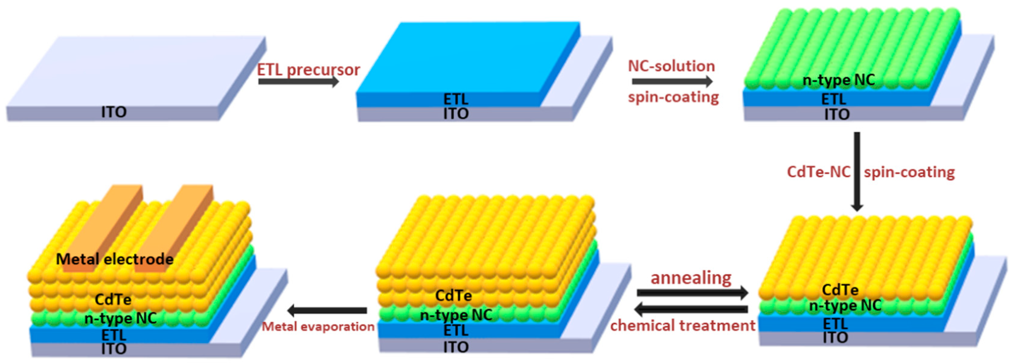
2. NC Solar Cell Fabrication Technology Determines the Electronic Properties

The size and morphology of CdTe NC thin film is quite different from that prepared by vacuum techniques. It is comprised of thousands of atoms. Therefore, the optical properties and bandgap of NC show a wide distribution due to the quantum size effects [9]. The assembly of CdTe NC during the fabrication of NC thin film is not perfect, and impurities within the surface of NC affect the optical and electrical properties of NC thin film [14,15,16]. In addition, the bandgap of bulk CdTe is ~1.45 eV, which is in the ideal bandgap region for single junction solar cells to achieve high efficiency. The decrease in size will shift the bandgap of NC to a wide region (>1.45 eV), which may affect the performance of NC solar cells. A chemical/annealing process is usually adopted to eliminate bulk defects in the CdTe NC thin film to increase the diffusion length of carriers. This is different from the fabrication of PbS quantum dots solar cells [17] under low temperatures (<100 °C). It is well known that CdCl2 treatment at ~400 °C can significantly improve the junction quality of CdTe thin film solar cells prepared by the close space submission (CSS) method [18,19]. However, as the grain size, melting point, or surface chemical properties of CdTe NC are quite different from those of CdTe thin film prepared by vacuum technology, the optimal chemical/annealing strategy should be different. To prepare CdTe NC thin film by solution processing, the first key issue is to obtain a well-dispersed NC solution. Thanks to the development of NC separation techniques, homogeneous CdTe NC solution can be prepared by refluxing the as-prepared NC to remove the impurities and insulated ligands and then disperse it into a solvent such as pyridine or deionized water [20,21]. In the early research, CdTe NC thin film was prepared by spin-casting a single layer of CdTe NC solution on the substrate and undergoing a chemical/annealing process [22]. The drawback of this method is that the increased stresses that develop during the annealing step may cause the formation of cracks, voids, and/or holes in the NC film, which will lead to device shunt or weaken in performance. Furthermore, the bulk defects in the CdTe NC thin film limit carrier transfer, and the solar cell PCEs are usually below 3% [23,24]. Recently, a layer-by-layer approach was adopted to overcome this problem [25,26]. As shown in Figure 1, this involves several drops of CdTe NCs solution being put on top of an ITO/ZnO/n type semiconductor (such as CdS, CdSe, or TiO2) substrate and spin-casted. Then, the substrate is placed on a hot plate and annealed at a temperature of ~150 °C for several minutes to eliminate any organic solvent. After that, the substrate is dipped into a saturated CdCl2/CH3OH solution for ~10 s and taken out, rinsed in n-propanol, and blow-dried under N2 flow. The substrate is then placed immediately on a hotplate at ~350 °C for ~10–60 s. This process permits the growth of CdTe NC into larger sizes (typically ~100 nm), which is important to decrease the interface defects between NC grains. This NC thin film fabrication process is repeated for several cycles in order to obtain CdTe NC thin film with the desired thickness. In general, 5–7 layers are needed to obtain an optimal thickness for light harvesting. This layer-by-layer approach can alleviate stresses in each layer, and the residual defects are filled by the subsequent layers. The high quality CdTe NC thin film obtained in this case is beneficial for carrier transfer, and high device performance is expected. On the other hand, this technique permits the electronic properties of each layer to be adjusted, which is important for efficient solar cell design. At present, most efficient CdTe NC based solar cells are fabricated by this layer-by-layer technique; it is a widely mastered method that produces CdTe NC thin film with a smooth, compact, and low-defect surface.

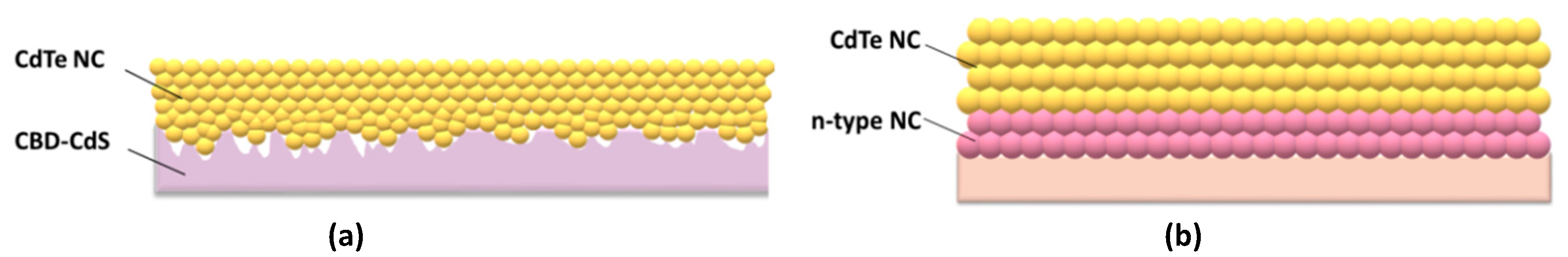
3. Improving p–n Junction Quality by Using an n-Type NC Partner

CdTe can exist easily in both n- and p-type materials by controlling the doping concentration of Cd or Te during thin film formation. However, due to the self-compensation effect, n-type CdTe is not stable; therefore, efficient polycrystalline CdTe thin-film solar cells are generally fabricated with p–n heterojunction configurations to effectively collect photo-carriers from devices in which the diffusion coefficients are small [27,28]. As confirmed in the literature, CdTe NC thin film remains a weak p-type with a hole concentration of around 1015/cm3 [29]. The first completely solution-processed NC solar cells with a PCE of 2.9 % in a configuration of ITO/CdTe/CdSe/Au were fabricated by employing CdTe and CdSe NCs as donor and acceptor materials [23]. The solar cells were fabricated by depositing one layer of CdTe NC and one layer of CdSe NC on the ITO substrate and annealing at 400 °C with CdCl2/methanol solution. Later on, the effect of the selected electrode or thickness of NC on the device’s performance was further investigated and similar device performances were obtained [30,31]. There are several obvious drawbacks for these NC solar cells. The charge-separating interface is far from the illumination, which results in high recombination, as the carriers must travel almost the whole active layer before they are collected. On the other hand, the CdTe/CdSe NC active layers are over-treated, leading to unexpected carrier recombination due to large defects in the NC thin film. Following this, a layer-by-layer approach was adopted to fabricate CdTe NC/ZnO heterojunction solar cells with a configuration of ITO/CdTe/ZnO/Al [32,33,34]. In this process, the n-type partner ZnO thin film is fabricated by depositing Zn2+ precursor on the CdTe thin film and annealing at a moderate temperature of ~300 °C. The optimized annealing temperature for CdTe NC thin film is ~350 °C. A further increase or decrease in the annealing temperature will deteriorate the performance of the CdTe NC thin film solar cells, resulting in device shunt or inadequate annealing, leading to poor NC grain size. When the ZnO was replaced by In-doped ZnO, a PCE of 8.54% was recorded [29], which was a drastic improvement comparing with previous work. Researchers also found that the PCE can be further elevated to 12% via light/current treatment. Unfortunately, the PCE will degrade in one day due to the recovery of energy obstacles for carrier transfer from CdTe to the ITO electrode. It is found that interdiffusion from the ITO into the CdTe layer at temperature higher than 250 °C may result in unfavorable electronic doping in CdTe NC film [14,15,16]. To overcome this drawback, introducing metal oxide, Au, ZnTe:Cu or Te interlayers between CdTe NC and ITO will significantly improve stability of CdTe NC solar cells with normal structure [35,36,37]. It is noted that the grain size of CdTe NC is around ~100 nm after chemical/heat-treatment. On the contrary, the typical n-type partner for CdTe thin film solar cells prepared by the chemical bath deposition (CBD) method, CdS, showed significantly larger grain sizes (several μm) and poor smoothness when compared with CdTe NC thin film. As shown in Figure 2a, when CdTe NCs are deposited on CBD-CdS thin film, lots of pin holes may be generated due to the mismatch in grain size between CdTe NC and CBD CdS, which reduces the junction quality of CdTe–CdS. On the contrary, a smooth and compact thin film is obtained when CdS NC ink is adopted (as shown in Figure 2b), which is important to eliminate interface defects and decrease carrier recombination in the interface.
In previous work [25], it was found that after optimizing the annealing temperature and the thickness of CdS NC film, a device with a configuration of ITO/ZnO/CdS NC/CdTe NC/Au showed a PCE of 5.14%, which is significantly higher than that of devices with CBD-CdS as an n-type partner (3.73%) [38]. The improvement in device performance was mainly attributed to the increases in fill factor (FF) and short circuit current density (Jsc). Besides CdS NC, CdSe NC has also been selected as an n-type partner for CdTe NC solar cells. The bandgap of bulk CdSe is about 1.7 eV, which does not lead to efficient CdTe thin film solar cells due to parasitic absorption of the CdSe layer. However, as the diffusion of Se into Te occurs more easily than S into Te, a CdSexTe1−x alloy layer can be easily formed when growing and post-treating the CdTe/CdSe thin film [39,40]. Due to the “light bowing” effects, CdSexTe1−x shows a narrower bandgap than that of CdTe, which will extend the spectrum response to a longer wavelength [41,42], and a higher Jsc is expected in this case. The CdTe/CdSe solar cells prepared through magnetron sputtering techniques show a high efficiency of 15.2% coupled with a high Jsc of 26.3 mA/cm2 [43]. Researchers have shown that the photo-currents are enhanced in both short and long wavelength regions when CdS is replaced by CdSe in the CdTe thin film solar cells [44]. In the early work of solution-processed CdTe/CdSe NC solar cells [22,45], however, similar improvement in photo-current were not found, which was mainly attributed to the device architecture and device fabrication techniques used. In the CdTe NC device with a normal ITO/CdTe/CdSe/Al structure, the junction is far from the illumination and the CdSe NC layer acts as an electronic transfer layer. The light absorbed by the CdSe NC layer will not generate any photonic current due to the interface recombination. Recently, a new inverted device structure (ITO/ZnO/CdSe/CdTe/Au) was developed using a layer-by-layer sintering process [46]. In this device structure, the presence of the ZnO layer provides better electrical stability, eliminating the catastrophic shorting of CdTe NC solar cells. As the CdTe NC has a similar size, morphology, and lattice structure as that of CdSe NC, a high junction quality is preferred when the NC thin film is treated under suitable conditions. Furthermore, the formation of the CdSexTe1−x layer is photo active, which will increase the external quantum efficiency (EQE) value in both short and long wavelengths. By optimizing the CdSe NC layer thickness and annealing temperature, a PCE of 5.81% was obtained in the champion devices. From the EQE spectrum, one can see that the device showed a good spectrum response in the short and long wavelength regions, which is in accordance with the previous report [41]. Due to the toxicity of the Cd element, using safer salts (such as NaCl, KCl or NH4Cl) instead of CdCl2 during the processing steps is believed to be important for decreasing the Cd contamination during the NC solar cells fabrication [8,47,48,49]. On the other hand, finding a new Cd-free n-type partner is also preferred for CdTe NC solar cells. Recently, solution-processed ZnSe NC was introduced as an n-type partner for CdTe NC solar cells [50]. However, compared to CdTe/CdSe, CdTe/ZnSe shows a lower junction quality and device performance. For the CdTe NC/TiO2 solar cells, the mismatch in crystalline lattice parameters between CdTe and TiO2 leads to large interface defects. To solve this problem, a thin layer of CdS NC (~5 nm) is deposited on the TiO2 film before deposition of the CdTe NC layer, which decreases the interface defects as CdS NC has a similar size and morphology to CdTe NC. The efficiency of CdTe NC solar cells increases to 5.14%, which is significantly higher than that of solar cells without the CdS NC interlayer [51]. A high Voc of up to 0.83 V is obtained in this case, which is the highest Voc for CdTe NC-based solar cells. The improvement in Voc is mainly attributed to the high junction quality and ideal band alignment.

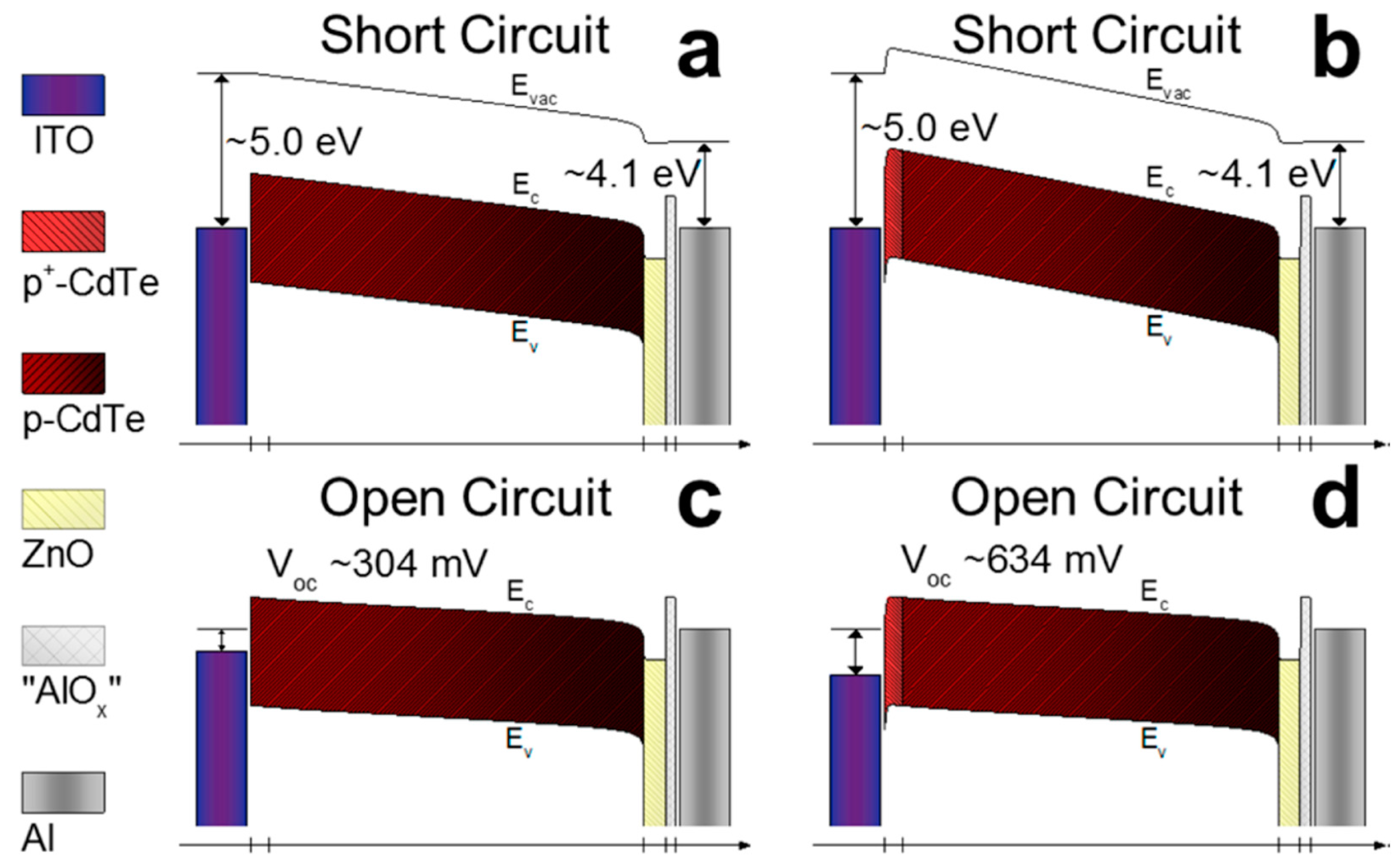
4. Back Contact for CdTe NC Solar Cells

It is well known that the CdTe thin film has high resistance due to the difficulty in element doping. Furthermore, the work function of CdTe thin film can be as high as 5.7 eV [50] and no metal exists that has a higher work function to form stable and low resistance contact than CdTe. In order to decrease the electric energy loss and maximize the voltage output, energy level matching between CdTe and the contact electrode is of fundamental importance. In general, the surface of CdTe is etched with nitric and phosphoric acids or Br2/methanol solution to generate a Te-rich interface which helps to form low resistance ohmic contacts [52,53]. However, compared to CdTe thin film fabricated by the vacuum technique, the grain size is small, and a high crystal boundary exists in solution-processed CdTe NC thin film. The acid molecules will move quickly along the crystal boundary and damage the whole NC thin film, leading to device shunt or thin film peeling off the substrate, which has been confirmed in previous work [33]. For a device with normal structure, by using chemical wet etching, the energy obstacle between ITO and CdTe NC film is eliminated and leads to the highest efficiency CdTe solution processed solar cell with a PCE of 12.7% [8,47,48,49]. For devices with inverted structure, the use of dielectric materials as a hole transport layer (HTL) before the deposition of back contact is also preferred to obtain low ohmic contact to CdTe NC. For example, by using high work function MoOx as the HTL, electrons are blocked while holes can transfer easily from CdTe to the gold electrode, which is essential to reduce carrier recombination on the interface of CdTe NC and to improve the device’s performance [25]. Organic hole transport materials can also be used as the HTL for CdTe NC solar cells for low-temperature and low-cost solution processing. Yang et al. first developed p-type Spiro[9H-fluorene-9,9′-[9H]xanthene]-2,2′,7,7′-tetramine (spiro-OMeTAD)as an HTL for solution-processed CdTe NC solar cells, and an improvement in open circuit voltage was obtained compared to devices with other HTLs [54]. It was found that the soft base spiro-OMeTAD bonds tightly to the CdTe atoms and forms a dipole layer, which is essential to decrease interface defects in the NC solar cells. The electrical potential between the HTL and the CdTe layer was investigated by Kelvin probe microscopy, and it was found that the dipole moment pointed toward the anode, which reinforces the Vbi (build in field) and facilitates carrier collection. Following this, the commercially available polyelectrolyte poly-[3-(potassium-6-hexanoate) thiophene-2, 5-diyl] (P3KT) was used as the HTL to improve the performance of aqueous-processed CdTe NC solar cells [55]. P3KT polyelectrolytes possess suitable energy levels that match well with CdTe, and the S atoms on the polymer backbone can coordinate with the CdTe NCs, which can reduce interfacial recombination and facilitate hole transfer and collection. By further introducing P3KT/MoOx double HTLs, a PCE of 5.9% was obtained. It is noted that the Highest Occupied Molecular Orbital (HOMO) level of the polymer mentioned above is ~5.2 eV, which is still lower than that of CdTe NC film (~5.3 eV). To solve this problem, HTL materials with higher HOMO levels are preferred. Triphenylamine-based conjugated polymers are excellent hole transfer materials with a high HOMO level, and they have been widely used in organic solar cells as an HTL [3,56]. Recently, a new organic hole transport material, poly(diphenylsilane-co-4-vinyl-triphenylamine) (Si–TPA), was used as the hole transport layer (HTL) for CdTe NC solar cells [57]. Its HOMO value is ~5.4 eV, which matches well with the VB of CdTe NC thin film. Studies have shown that Si–TPA can bond to the CdTe NC film by forming N–Cd covalent bonds, and the hole mobility in bulk is enhanced for NC devices. For comparison, poly(9-vinylcarbazole) (PVK) and poly(3,4-ethylenedioxythiophene):poly(styrenesulfonate) (PEDOT:PSS) were also used as HTLs for CdTe NC solar cells. Although PEDOT:PSS and PVK have similar energy levels to Si-TPA, their film quality is low due to the lack of strong dangling bonds, leading to low device performance. On the contrary, due to the dipole effects and ideal band alignment, devices with Si–TPA HTL show significantly higher Jsc and Voc values, leading to a higher PCE of 8.34%, which is the highest ever reported for solution-processed CdTe NC solar cells with an inverted structure. The selected performance parameters of solution processed CdTe NC based solar cells are summarized in Table 1.

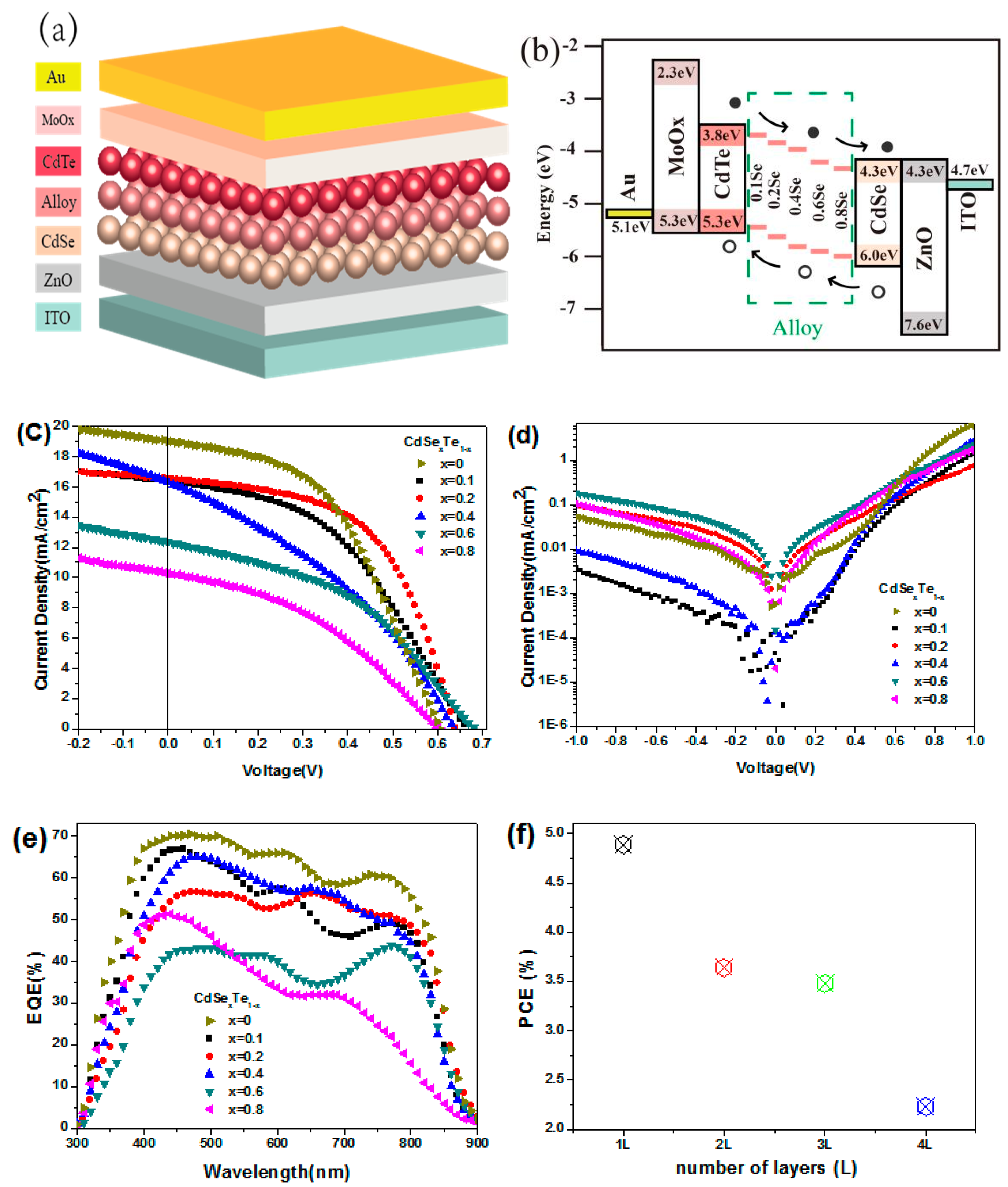
5. The Architecture Design and Combinations of New Devices

Although the band gap of CdTe NC thin film (~1.45 eV) is in the ideal bandgap region for single junction solar cells according to the Shockley−Queisser constraint [64], to further improve device performance, a higher Jsc is preferred. One way to improve the short circuit current of NC solar cells is to introduce more active layers with a lower bandgap. For example, introducing more CdSexTe1−x NC active layers into the CdTe NC solar cells will extend the spectrum response to the longer wavelength region, as CdSexTe1−x layers possess a lower bandgap (less than 1.45 eV). There are several ways to attain a CdSexTe1−x alloy NC active layer. For example, sintering thin films containing mixtures of CdTe and CdSe NC will form CdSexTe1-x alloy easily due to the low melting point of NC [24,45]. In this case, a mixture of different compositions of CdTe and CdSe NC is deposited on the substrate and annealed at a temperature of ~350 °C to facilitate the formation of CdSexTe1−x alloy. Improved device performance is obtained in this case, which is mainly attributed to an increase in Jsc. It is also found that the device performance can be tuned by adjusting the composition of the NC alloy. Later on, the CdSexTe1−x alloy NC is used directly to replace the mixtures of CdTe and CdSe NCs as the active layer [61]. Here, a homogeneous alloy active layer is obtained through the application of CdSexTe1−x NC with an ascertained composition. Furthermore, as the physical properties of each active layer can be well controlled, the NC performance can be adjusted easily. As shown in Figure 3a, NC solar cells with a vertically-graded bandgap are formed using the layer-by-layer NC deposition process. In this new device architecture, the active layer consists of two or more alloy NC layers with different bandgaps, which will extend the absorption range. Furthermore, as shown in Figure 3b, the slope of the built-in electric field will facilitate carrier separation and collection. The device performance is found to be related to composition of alloy, as shown in Figure 3c,d. Due to the present of low band gap CdxTe1−x alloy, enhanced EQE is found in both short and long wavelength when comparing to traditional CdTe-CdS NC solar cells (Figure 3e) [38]. The performance of alloy NC solar cells is also found to be related to the thickness of active layer (Figure 3f), the device architecture, and the quantity of alloy active layers used. In optimized device structure of ITO/ZnO/ CdSe0.8Te0.2/CdSe0.2Te0.8/CdTe/MoOx/Au, the series resistance (Rs) is decreased and the shunt resistance (Rsh) increased when comparing to device with structure of ITO/ZnO/CdSe0.2Te0.8/CdTe/MoOx/Au, which results in a high PCE of 6.37% (4.03% for controlled device) [61].
Introducing other semiconductor NC or organic semiconductor materials to build tandem solar cells is another way to further improve the performance of CdTe NC solar cells. PbS quantum dots are important semiconductor materials for photovoltaic application as the band gap can be tuned from the bulk value (0.41 eV) up to ~1.6 eV by controlling the grain size [65,66]. The efficiency of PbS quantum dot solar cells has improved from ~0.1% to ~11% in recent years [4]. As the optical absorption of PbS quantum dots can be extended to the infrared region, coupled with low temperature device fabrication, all these merits make PbS quantum dots solar cells (CQDs) suitable for application in tandem cells. Crisp et al. demonstrated new tandem solar cells based on solution-processed CdTe NCs and PbS CQDs [67]. The device structure was FTO/CdS/CdTe/ZnTe/ZnO/PbS/MoOx/Al. It was found that the ZnTe/ZnO tunnel junction is appropriate to combine the CdTe and PbS cells, and a Voc as high as 1.1 V can be obtained in the optimized device. This value is significantly higher than that of the the single CdTe (~0.6 V) and PbS (~0.4 V) solar cells. However, the overall conversion efficiency is only 5%, which is significantly lower than that of the best CdTe NC solar cells (~11%) or PbS CQD solar cells (~12%). The low PCE is mainly attributed to the low Jsc (~10 mA/cm2). The low EQE response of the whole spectrum indicates that much work should be done to improve the film quality of every active layer.

6. Outlook

Unlike the traditional CdTe thin film solar cells fabricated from the evaporation of semiconductor materials to construct an active layer, CdTe NC solar cells are prepared by a simple layer-by-layer solution and sintering process. Therefore, the electronic properties of NC thin film can be rationally controlled by varying the thin film fabricating method. The highest and most stable PCE of solution-processed CdTe NC based solar cells obtained is around 9%; there still exists great potential for commercial application. To further improve the efficiency up to 15%, more research should be done. Firstly, the Voc of most CdTe NC solar cells is around 0.6–0.7 V, which is significantly lower than most CdTe thin film solar cells prepared by CSS or other vacuum techniques (~0.8–0.9 V). As the carrier doping concentration for CdTe NC thin film is ~1015/cm3, it is difficult to make good ohmic contact without further interface treatment or increased doping density. Creating a Te-rich layer is therefore important to create good ohmic contact to further increase the performance of the NC solar cells. Unfortunately, there are still no reports on the successful application of these methods to solution-processed CdTe NC solar cells. In a previous report, Panthani et al [29] attempted to create a Te-rich layer by wet-etching the CdTe NC thin film; the device showed exclusively shunt action and no efficiency. Therefore, a new chemical etching method must be developed to further improve the ohmic back contact to CdTe NC thin film. In the previous reports, introducing a interlayer (such as ZnTe:Cu or Te) between ITO and CdTe NC thin film has led to significantly improvement in performance of CdTe NC solar cells [36]. As shown in Figure 4a–d, by modeling heavily doped CdTe at the interface between ITO and the CdTe NC thin film, a good Ohmic contact to CdTe is formed, which can significantly improve the CdTe NC based solar cells [12]. How to apply this technology to inverted NC solar cells is a still challenge. On the other hand, increasing the doping concentration of CdTe NC thin film is also crucial to further improve the performance of NC solar cells. In previous work, ZnTe:Cu or CuxTe was selected as the back contact for NC solar cells and a PCE of ~6% was obtained [24]. The low PCE is mainly attributed to the low Jsc, which is due to the absorption of the n-type partner. By using a solution-processed n-type semiconductor NC and optimizing the Cu doping in the CdTe NC thin film, the PCE of NC solar cells could improve towards 10%. Recently, Dharmadasa et al. [68] and our group developed a new device structure with a graded bandgap structure. In this device structure, the separation of photo-generated charge carriers is easy, and the spectrum response is extended. More work should be done to further optimize each active layer to further improve the spectrum response to the long wavelength region and to improve the performance of NC solar cells towards 15%. In order to realize the commercial application of CdTe NC solar cells, improved stability, material processing, and scale-up fabricating techniques (such as inkjet printing or spray coating) are required. However, due to their simple, low-cost fabrication techniques and low material consumption, CdTe NC-based solar cells have a promising future.

Author Contributions

D.Q., K.L. and W.W. examined the literature; D.Q., K.L., W.W., S.X., Y.J. and S.L. compiled the paper.

Funding

This research received no external funding.

Acknowledgments

We thank the financial support of the National Natural Science Foundation of China (No. 21875075, 61774077, 61274062, 61775061), Guangdong Province Natural Science Fund (No. 2018A0303130041), Guangzhou Science and Technology Plan Project (No. 201804010295), National Undergraduate Innovative and Entrepreneurial Training Program (No. 201810561013).

Conflicts of Interest

The authors declare no conflict of interest.

References

  1. Meng, L.X.; Zhang, Y.M.; Wan, X.J.; Li, C.X.; Zhang, X.; Wang, Y.B.; Ke, X.; Xiao, Z.; Ding, L.M.; Xia, R.X.; et al. Organic and solution-processed tandem solar cells with 17.3% efficiency. Science 2018, 361, 1094–1098. [Google Scholar] [CrossRef]
  2. Xue, Q.F.; Bai, Y.; Liu, M.Y.; Xia, R.X.; Hu, Z.C.; Chen, Z.M.; Jiang, X.F.; Huang, F.; Yang, S.H.; Matsuo, Y.; et al. Dual interfacial modifications enable high performance semitransparent perovskite solar cells with large open circuit voltage and fill factor. Adv. Energy Mater. 2017, 7, 1602333. [Google Scholar] [CrossRef]
  3. Rong, Y.G.; Hu, Y.; Mei, A.Y.; Tan, H.R.; Saidaminov, M.I.; Seok, S.I.; McGehee, M.D.; Sargent, E.H.; Han, H.W. Challenges for commercializing perovskite solar cells. Science 2018, 361, eaat8235. [Google Scholar] [CrossRef] [PubMed]
  4. Kim, J.; Ouellette, O.; Voznyy, O.; Wei, M.; Choi, J.; Choi, M.J.; Jo, J.; Beak, S.W.; Fan, J.; Saidaminov, M.I.; et al. Butylamine-Catalyzed Synthesis of Nanocrystal Inks Enables Efficient Infrared CQD Solar Cells. Adv. Mater. 2018, 30, 1803830. [Google Scholar] [CrossRef]
  5. Kim, Y.; Che, F.; Jo, J.W.; Choi, J.; García de Arquer, F.P.; Voznyy, O.; Sun, B.; Kim, J.; Choi, M.-J.; Quintero-Bermudez, R.; et al. A Facet-Specific Quantum Dot Passivation Strategy for Colloid Management and Efficient Infrared Photovoltaics. Adv. Mater. 2019, 31, 1805580. [Google Scholar] [CrossRef] [PubMed]
  6. Hou, W.W.; Bob, B.; Li, S.H.; Yang, Y. Low-temperature processing of a solution-deposited CuInSSe thin-film solar cell. Thin Solid Films 2009, 517, 6853–6856. [Google Scholar] [CrossRef]
  7. Kranz, L.; Gretener, C.; Perrenoud, J.; Jaeger, D.; Gerstl, S.S.; Schmitt, R.; Buecheler, S.; Tiwari, A.N. Tailoring impurity distribution in polycrystalline CdTe solar cells for enhanced minority carrier lifetime. Adv. Energy Mater. 2014, 4, 1301400. [Google Scholar] [CrossRef]
  8. Major, J.D.; Treharne, R.E.; Phillips, L.J.; Durose, K. A low-cost non-toxic post-growth activation step for CdTe solar cells. Nature 2014, 511, 334. [Google Scholar] [CrossRef]
  9. Yu, W.W.; Wang, Y.A.; Peng, X. Formation and stability of size-, shape-, and structure-controlled CdTe nanocrystals: Ligand effects on monomers and nanocrystals. Chem. Mater. 2003, 15, 4300–4308. [Google Scholar] [CrossRef]
  10. Peng, Z.A.; Peng, X. Formation of high-quality CdTe, CdSe, and CdS nanocrystals using CdO as precursor. J. Am. Chem. Soc. 2001, 123, 183–184. [Google Scholar] [CrossRef]
  11. Jiang, Y.; Xu, S.; Zhao, Z.; Zheng, L.; Wang, Z.; Wang, C.; Cui, Y. Water–ethanol solvent mixtures: A promising liquid environment for high quality positively-charged CdTe nanocrystal preparation. RSC Adv. 2015, 5, 18379–18383. [Google Scholar] [CrossRef]
  12. Sun, S.; Liu, H.; Gao, Y.; Qin, D.; Chen, J. Controlled synthesis of CdTe nanocrystals for high performanced Schottky thin film solar cells. J. Mater. Chem. 2012, 22, 19207–19212. [Google Scholar] [CrossRef]
  13. Yuan, M.J.; Liu, M.X.; Sargent, E.H. Colloidal quantum dot solids for solution-processed solar cells. Nat. Energy 2016, 1, 16016. [Google Scholar] [CrossRef]
  14. Zhang, H.; Kurley, J.M.; Russell, J.C.; Jang, J.; Talapin, D.V. Solution-Processed, Ultrathin Solar Cells from CdCl3-Capped CdTe Nanocrystals: The Multiple Roles of Cdcl3- Ligands. J. Am. Chem. Soc. 2016, 138, 7464–7467. [Google Scholar] [CrossRef] [PubMed]
  15. Jang, J.; Dolzhnikov, D.S.; Liu, W.; Nam, S.; Shim, M.; Talapin, D.V. Solution-Processed Transistors Using Colloidal Nanocrystals with Composition-Matched Molecular “Solders”: Approaching Single Crystal Mobility. Nano Lett. 2015, 15, 6309–6317. [Google Scholar] [CrossRef] [PubMed]
  16. Crisp, R.W.; Callahan, R.; Reid, O.G.; Dolzhnikov, D.S.; Talapin, D.V.; Rumbles, G.; Luther, J.M.; Kopidakis, N. Photoconductivity of CdTe Nanocrystal-Based Thin Films: Te2-Ligands Lead to Charge Carrier Diffusion Lengths over 2 µm. J. Phys. Chem. Lett. 2015, 6, 4815–4821. [Google Scholar] [CrossRef]
  17. Lan, X.; Voznyy, O.; García de Arquer, F.P.; Liu, M.; Xu, J.; Proppe, A.H.; Walters, G.; Fan, F.J.; Tan, H.R.; Liu, M. 10.6% certified colloidal quantum dot solar cells via solvent-polarity-engineered halide passivation. Nano Lett. 2016, 16, 4630–4634. [Google Scholar] [CrossRef]
  18. Rios-Flores, A.; Pena, J.L.; Castro-Pena, V.; Ares, O.; Castro-Rodríguez, R.; Bosio, A. A study of vapor CdCl2 treatment by CSS in CdS/CdTe solar cells. Sol. Energy 2012, 84, 1020–1026. [Google Scholar] [CrossRef]
  19. Vigil-Galán, O.; Arias-Carbajal, A.; Mendoza-Pérez, R.; Santana-Rodríguez, G.; Sastre-Hernández, J.; Alonso, J.C.; Moreno-Garcia, E.; Contreras-Puente, G.; Morales-Acevedo, A. Improving the efficiency of CdS/CdTe solar cells by varying the thiourea/CdCl2 ratio in the CdS chemical bath. Semicond. Sci. Technol. 2015, 20, 819. [Google Scholar] [CrossRef]
  20. Tong, S.W.; Mishra, N.; Su, C.L.; Nalla, V.; Wu, W.; Ji, W.; Zhang, J.; Chan, Y.; Loh, K.P. High-performance hybrid solar cell made from CdSe/CdTe nanocrystals supported on reduced graphene oxide and PCDTBT. Adv. Funct. Mater. 2014, 24, 1904–1910. [Google Scholar] [CrossRef]
  21. Li, Y.C.; Zhong, H.Z.; Li, R.; Zhou, Y.; Yang, C.H.; Li, Y.F. High-yield fabrication and electrochemical characterization of tetrapodal CdSe, CdTe, and CdSexTe1–x nanocrystals. Adv. Funct. Mater. 2006, 16, 1705–1716. [Google Scholar] [CrossRef]
  22. Gur, I.; Fromer, N.A.; Geier, M.L.; Alivisatos, A.P. Air-stable all-inorganic nanocrystal solar cells processed from solution. Science 2005, 310, 462–465. [Google Scholar] [CrossRef]
  23. Anderson, I.E.; Breeze, A.J.; Olson, J.D.; Yang, L.; Sahoo, Y.; Carter, S.A. All-inorganic spin-cast nanoparticle solar cells with nonselective electrodes. Appl. Phys. Lett. 2009, 94, 063101. [Google Scholar] [CrossRef] [Green Version]
  24. Tan, F.; Qu, S.; Zhang, W.; Wang, Z. Hybrid morphology dependence of CdTe: CdSe bulk-heterojunction solar cells. Nanoscale Res. Lett. 2014, 9, 593. [Google Scholar] [CrossRef] [PubMed]
  25. Liu, S.W.; Liu, W.G.; Heng, J.X.; Zhou, W.F.; Chen, Y.R.; Wen, S.Y.; Qin, D.H.; Hou, L.T.; Wang, D.; Xu, H. Solution-Processed Efficient Nanocrystal Solar Cells Based on CdTe and CdS Nanocrystals. Coatings 2018, 8, 26. [Google Scholar] [CrossRef]
  26. Jasieniak, J.; MacDonald, B.I.; Watkins, S.E.; Mulvaney, P. Solution-processed sintered nanocrystal solar cells via layer-by-layer assembly. Nano Lett. 2011, 11, 2856–2864. [Google Scholar] [CrossRef]
  27. Chu, T.L.; Chu, S.S.; Ferekides, C.; Wu, C.Q.; Britt, J.; Wang, C. 13.4% efficient thin-film CdS/CdTe solar cells. J. Appl. Phys. 1991, 70, 7608–7612. [Google Scholar] [CrossRef]
  28. Kumar, S.G.; Rao, K.K. Physics and chemistry of CdTe/CdS thin film heterojunction photovoltaic devices: Fundamental and critical aspects. Energy Environ. Sci. 2014, 7, 45–102. [Google Scholar] [CrossRef]
  29. Panthani, M.G.; Kurley, J.M.; Crisp, R.W.; Dietz, T.C.; Ezzyat, T.; Luther, J.M.; Talapin, D.V. High efficiency solution processed sintered CdTe nanocrystal solar cells: The role of interfaces. Nano Lett. 2014, 14, 670–675. [Google Scholar] [CrossRef]
  30. Townsend, T.K.; Yoon, W.; Foos, E.E.; Tischler, J.G. Impact of nanocrystal spray deposition on inorganic solar cells. ACS Appl. Mater. Interfaces 2014, 6, 7902–7909. [Google Scholar] [CrossRef]
  31. Yoon, W.; Townsend, T.K.; Lumb, M.P.; Tischler, J.G.; Foos, E.E. Sintered CdTe nanocrystal thin films: Determination of optical constants and application in novel inverted heterojunction solar cells. IEEE Trans. Nanotechnol. 2014, 13, 551–556. [Google Scholar] [CrossRef]
  32. MacDonald, B.I.; Della Gaspera, E.; Watkins, S.E.; Mulvaney, P.; Jasieniak, J.J. Enhanced photovoltaic performance of nanocrystalline CdTe/ZnO solar cells using sol-gel ZnO and positive bias treatment. J. Appl. Phys. 2014, 115, 184501. [Google Scholar] [CrossRef]
  33. Crisp, R.W.; Panthani, M.G.; Rance, W.L.; Duenow, J.N.; Parilla, P.A.; Callahan, R.; Dabney, M.S.; Berry, J.J.; Talapin, D.V.; Luther, J.M. Nanocrystal grain growth and device architectures for high-efficiency CdTe ink-based photovoltaics. ACS Nano 2014, 8, 9063–9072. [Google Scholar] [CrossRef]
  34. MacDonald, B.I.; Gengenbach, T.R.; Watkins, S.E.; Mulvaney, P.; Jasieniak, J.J. Solution-processing of ultra-thin CdTe/ZnO nanocrystal solar cells. Thin Solid Films 2014, 558, 365–373. [Google Scholar] [CrossRef]
  35. Chambers, B.A.; MacDonald, B.I.; Ionescu, M.; Deslandes, A.; Quinton, J.S.; Jasieniak, J.J.; Andersson, G.G. Examining the Role of Ultra-Thin Atomic Layer Deposited Metal Oxide Barrier Layers on CdTe/ITO Interface Stability during the Fabrication of Solution Processed Nanocrystalline Solar Cells. Sol. Energy Mater. Sol. Cells 2014, 125, 164–169. [Google Scholar] [CrossRef]
  36. Kurley, J.M.; Panthani, M.G.; Crisp, R.W.; Nanayakkara, S.U.; Pach, G.F.; Reese, M.O.; Hudson, M.H.; Dolzhnikov, D.S.; Tanygin, V.; Luther, J.M.; et al. Transparent Ohmic Contacts for Solution-Processed, Ultrathin CdTe Solar Cells. ACS Energy Lett. 2017, 2, 270–278. [Google Scholar] [CrossRef]
  37. Zhu, J.; Yang, Y.; Gao, Y.; Qin, D.; Wu, H.; Hou, L.; Huang, W. Enhancement of Open-Circuit Voltage and the Fill Factor in CdTe Nanocrystal Solar Cells by Using Interface Materials. Nanotechnology 2014, 25, 365203. [Google Scholar] [CrossRef]
  38. Tian, Y.Y.; Zhang, Y.J.; Lin, Y.Z.; Gao, K.; Zhang, Y.P.; Liu, K.Y.; Yang, Q.Q.; Zhou, X.; Qin, D.H.; Wu, H.B.; et al. Solution-processed efficient CdTe nanocrystal/CBD-CdS hetero-junction solar cells with ZnO interlayer. J. Nanopart. Res. 2013, 15, 2053. [Google Scholar] [CrossRef]
  39. Bao, Z.; Yang, X.Y.; Li, B.; Luo, R.; Liu, B.; Tang, P.; Zhang, J.Q.; Wu, L.L.; Li, W.; Feng, L.H. The study of CdSe thin film prepared by pulsed laser deposition for CdSe/CdTe solar cell. J. Mater. Sci.: Mater. Electron. 2016, 27, 7233–7239. [Google Scholar] [CrossRef]
  40. Swanson, D.E.; Sites, J.R.; Sampath, W.S. Co-sublimation of CdSexTe1−x layers for CdTe solar cells. Sol. Energy Mater. Sol. Cells 2017, 159, 389–394. [Google Scholar] [CrossRef]
  41. Yang, X.Y.; Bao, Z.; Luo, R.; Liu, B.; Tang, P.; Li, B.; Zhang, J.Q.; Li, W.; Wu, L.L.; Feng, L.H. Preparation and characterization of pulsed laser deposited CdS/CdSe bi-layer films for CdTe solar cell application. Mater. Sci. Semicond. Process. 2016, 48, 27–32. [Google Scholar] [CrossRef]
  42. Yang, X.Y.; Liu, B.; Li, B.; Zhang, J.Q.; Li, W.; Wu, L.L.; Feng, L.H. Preparation and characterization of pulsed laser deposited a novel CdS/CdSe composite window layer for CdTe thin film solar cell. Appl. Surf. Sci. 2016, 367, 480–484. [Google Scholar] [CrossRef] [Green Version]
  43. Paudel, N.R.; Poplawsky, J.D.; Moore, K.L.; Yan, Y. Current enhancement of CdTe-based solar cells. IEEE J. Photovolt. 2015, 5, 1492–1496. [Google Scholar] [CrossRef]
  44. Paudel, N.R.; Yan, Y. Enhancing the photo-currents of CdTe thin-film solar cells in both short and long wavelength regions. Appl. Phys. Lett. 2014, 105, 183510. [Google Scholar] [CrossRef] [Green Version]
  45. MacDonald, B.I.; Martucci, A.; Rubanov, S.; Watkins, S.E.; Mulvaney, P.; Jasieniak, J.J. Layer-by-layer assembly of sintered CdSexTe1–x nanocrystal solar cells. ACS Nano 2012, 6, 5995–6004. [Google Scholar] [CrossRef]
  46. Liu, H.; Tian, Y.Y.; Zhang, Y.J.; Gao, K.; Lu, K.K.; Wu, R.F.; Qin, D.H.; Wu, H.B.; Peng, Z.S.; Hou, L.T.; et al. Solution processed CdTe/CdSe nanocrystal solar cells with more than 5.5% efficiency by using an inverted device structure. J. Mater. Chem. C 2015, 3, 4227–4234. [Google Scholar] [CrossRef]
  47. Williams, B.L.; Major, J.D.; Bowen, L.; Keuning, W.; Creatore, M.; Durose, K. A Comparative Study of the Effects of Nontoxic Chloride Treatments on CdTe Solar Cell Microstructure and Stoichiometry. Adv. Energy Mater. 2015, 5, 1500554. [Google Scholar] [CrossRef]
  48. Kirkwood, N.; Monchen, J.O.V.; Crisp, R.W.; Grimaldi, G.; Bergstein, H.A.; du Fossé, I.; van der Stam, W.; Infante, I.; Houtepen, A.J. Finding and Fixing Traps in II-VI and III-V Colloidal Quantum Dots: The Importance of Z-Type Ligand Passivation. J. Am. Chem. Soc. 2018, 140, 15712–15723. [Google Scholar] [CrossRef] [PubMed]
  49. Townsend, T.K.; Heuer, W.B.; Foos, E.E.; Kowalski, E.; Yoon, W.; Tischler, J.G. Safer Salts for CdTe Nanocrystal Solution Processed Solar Cells: The Dual Roles of Ligand Exchange and Grain Growth. J. Mater. Chem. A 2015, 3, 13057–13065. [Google Scholar] [CrossRef]
  50. Visoly-Fisher, I.; Dobson, K.D.; Nair, J.; Bezalel, E.; Hodes, G.; Cahen, D. Factors affecting the stability of CdTe/CdS solar cells deduced from stress tests at elevated temperature. Adv. Funct. Mater. 2003, 13, 289–299. [Google Scholar] [CrossRef]
  51. Li, M.Z.; Liu, X.Y.; Wen, S.Y.; Liu, S.W.; Heng, J.X.; Qin, D.H.; Hou, L.T.; Wu, H.B.; Xu, W.; Huang, W.B. CdTe nanocrystal hetero-junction solar cells with high open circuit voltage based on Sb-doped TiO2 electron acceptor materials. Nanomaterials 2017, 7, 101. [Google Scholar] [CrossRef]
  52. Seymour, F.H.; Kaydanov, V.; Ohno, T.R.; Albin, D. Cu and CdCl2 influence on defects detected in CdTe solar cells with admittance spectroscopy. Appl. Phys. Lett. 2005, 87, 153507. [Google Scholar] [CrossRef]
  53. Oman, D.M.; Dugan, K.M.; Killian, J.L.; Ceekala, V.; Ferekides, C.S.; Morel, D.L. Device performance characterization and junction mechanisms in CdTe/CdS solar cells. Sol. Energy Mater. Sol. Cells 1999, 58, 361–373. [Google Scholar] [CrossRef]
  54. Du, X.H.; Chen, Z.L.; Liu, F.Y.; Zeng, Q.S.; Jin, G.; Li, F.H.; Yao, D.; Yang, B. Improvement in open-circuit voltage of thin film solar cells from aqueous nanocrystals by interface engineering. ACS Appl. Mater. Interfaces 2015, 8, 900–907. [Google Scholar] [CrossRef]
  55. Zeng, Q.S.; Hu, L.; Cui, J.; Feng, T.L.; Du, X.H.; Jin, G.; Liu, F.Y.; Ji, T.J.; Li, F.H.; Zhang, H.; et al. High-Efficiency Aqueous-Processed Polymer/CdTe Nanocrystals Planar Heterojunction Solar Cells with Optimized Band Alignment and Reduced Interfacial Charge Recombination. ACS Appl. Mater. Interfaces 2017, 9, 31345–31351. [Google Scholar] [CrossRef]
  56. Saidaminov, M.I.; Kim, J.; Jain, A.; Quintero-Bermudez, R.; Tan, H.; Long, G.; Tan, F.R.; Johnston, A.; Zhao, Y.; Voznyy, O.; et al. Suppression of atomic vacancies via incorporation of isovalent small ions to increase the stability of halide perovskite solar cells in ambient air. Nat. Energy 2018, 3, 648. [Google Scholar] [CrossRef]
  57. Guo, X.Z.; Tan, Q.X.; Liu, S.W.; Qin, D.H.; Mo, Y.Q.; Hou, L.T.; Liu, A.L.; Wu, H.B.; Ma, Y.G. High-efficiency solution-processed CdTe nanocrystal solar cells incorporating a novel crosslinkable conjugated polymer as the hole transport layer. Nano Energy 2018, 46, 150–157. [Google Scholar] [CrossRef]
  58. Ju, T.; Yang, L.; Carter, S. Thickness dependence study of inorganic CdTe/CdSe solar cells fabricated from colloidal nanoparticle solutions. J. Appl. Phys. 2010, 10, 104311. [Google Scholar] [CrossRef]
  59. Townsend, T.K.; Foos, E.E. Fully solution processed all inorganic nanocrystal solar cells. Phys. Chem. Chem. Phys. 2014, 16, 16458–16464. [Google Scholar] [CrossRef]
  60. Xie, Y.; Tan, Q.X.; Zhang, Z.T.; Lu, K.K.; Li, M.Z.; Xu, W.; Qin, D.H.; Zhang, Y.D.; Hou, L.T.; Wu, H.B. Improving performance in CdTe/CdSe nanocrystals solar cells by using bulk nano-heterojunctions. J. Mater. Chem. C 2016, 4, 6483–6491. [Google Scholar] [CrossRef]
  61. Wen, S.Y.; Li, M.Z.; Yang, J.Y.; Mei, X.L.; Wu, B.; Liu, X.L.; Heng, J.X.; Qin, D.H.; Hou, L.T.; Xu, W. Rationally controlled synthesis of CdSexTe1−x alloy nanocrystals and their application in efficient graded bandgap solar cells. Nano Mater. 2017, 7, 380. [Google Scholar] [CrossRef] [PubMed]
  62. Chen, Z.L.; Zeng, Q.S.; Liu, F.Y.; Jin, G.; Du, X.H.; Du, J.L.; Zhang, H.; Yang, B. Efficient inorganic solar cells from aqueous nanocrystals: The impact of composition on carrier dynamics. RSC Adv. 2015, 5, 74263–74269. [Google Scholar] [CrossRef]
  63. Mei, X.L.; Wu, B.; Guo, X.Z.; Liu, X.L.; Rong, Z.T.; Liu, S.W.; Chen, Y.R.; Qin, D.H.; Xu, W.; Hou, L.T.; et al. Efficient CdTe Nanocrystal/TiO2 Hetero-Junction Solar Cells with Open Circuit Voltage Breaking 0.8 V by Incorporating A Thin Layer of CdS Nanocrystal. Nanomaterials 2018, 8, 614. [Google Scholar] [CrossRef] [PubMed]
  64. Shockley, W.; Queisser, H.J. Detailed Balance Limit of Efficiency of p–n Junction Solar Cells. J. Appl. Phys. 1961, 32, 510–519. [Google Scholar] [CrossRef]
  65. Ip, A.H.; Thon, S.M.; Hoogland, S.; Voznyy, O.; Zhitomirsky, D.; Debnath, R.; Levina, L.; Rollny, L.R.; Carey, G.H.; Fischer, A.; et al. Hybrid passivated colloidal quantum dot solids. Nat. Nanotechol. 2012, 7, 577. [Google Scholar] [CrossRef] [PubMed]
  66. Labelle, A.J.; Thon, S.M.; Masala, S.; Adachi, M.M.; Dong, H.; Farahani, M.; Ip, A.H.; Fratalocchi, A.; Sargent, E.H. Colloidal quantum dot solar cells exploiting hierarchical structuring. Nano Lett. 2015, 15, 1101–1108. [Google Scholar] [CrossRef] [PubMed]
  67. Crisp, R.W.; Pach, G.F.; Kurley, J.M.; France, R.M.; Reese, M.O.; Nanayakkara, S.U.; MacLeod, B.A.; Talapin, D.V.; Beard, M.C.; Luther, J.M. Tandem solar cells from solution-processed CdTe and PbS quantum dots using a ZnTe–ZnO tunnel junction. Nano Lett. 2017, 17, 1020–1027. [Google Scholar] [CrossRef] [PubMed]
  68. Dharmadasa, I.; Ojo, A.; Salim, H.; Dharmadasa, R. Next generation solar cells based on graded bandgap device structures utilising rod-type nano-materials. Energies 2015, 8, 5440–5458. [Google Scholar] [CrossRef]
Figure 1. NC solar cells with inverted structure fabricated by a layer by layer solution process.
Applsci 09 01885 g001
Figure 2. NC solar cells fabricated by using (a) CBD-CdS or (b) CdS NC as buffer layer.
Applsci 09 01885 g002
Figure 3. (a) Schematic of the vertically-graded bandgap structure of ITO/ZnO/CdSe/CdSexTe1-x/CdTe/MoOx/Au, (b) energy diagram of the above devices, J-V characteristics of the above devices (c) under light and (d) dark, (e) EQE properties of the devices, and (f) the PCE of NC solar cells with different thickness of CdSe0.2Te0.8 alloy NC films [64].
Applsci 09 01885 g003
Figure 4. (a,c) Band diagrams of modeled CdTe solar cells with ITO/“CdTeOx”/CdTe/ZnO:In/ /“AlOx”/Al geometry at equilibrium (a) and Voc (c) before current/light soaking. (b,d) Band diagrams of modeled CdTe solar cells with a heavily doped CdTe layer between ITO and CdTe at equilibrium (b) and Voc (d) before current/light soaking [36]. Copyright 2017 American Chemical Society.
Applsci 09 01885 g004
Table 1. Selected performance parameters of CdTe NC solar cells fabricated via solution process.
StructureVoc (V)Jsc (mA/cm2)FF (%)PCE (%)Published YearRef
ITO/CdTe/ZnO/Al0.5920.7056.06.92011[26]
ITO/CdTe/ZnO/Al0.6121.2060.07..72014[34]
ITO/CdTe/ZnO/Al0.68625.5064.711.32014[33]
ITO/CdTe/In: ZnO/Al0.6921.2067.09.82014[32]
ITO/CdTe/In: ZnO/Al0.68425.8071.012.32014[29]
ITO/CdTe/CdSe/Al0.4216.9036.02.62009[23]
ITO/CdTe/CdSe/Al0.42916.3037.43.022010[58]
ITO/CdTe/CdSexTe1-x/ZnO/Al0.6120.357.07.12012[45]
ITO/CdSe/CdTe/Cr/Au0.5937.243.71.92014[31]
ITO/CdSe/CdTe/Au0.5617.240.13.752014[59]
ITO/ZnO/CdSe/CdTe/Au0.6515.2858.55.812015[46]
ITO/ZnO/CdSe/CdTe:CdSe/CdTe/Au0.621.0649.56.252016[60]
ITO/ZnO/CdSexTe1-x/CdTe/MoOx/Au0.6719.7048.36.372017[61]
ITO/ZnO/CdSe/CdTe/Si-TPA/Au0.6623.3854.058.342018[57]
ITO/TiO2/CdTe/spiro-OMeTAD/Au0.7115.8245.25.162015[54]
ITO/TiO2/CdTe-CdS/MoOx/Au0.56417.857.15.732015[62]
ITO/ZnO/Sb:TiO2/CdTe/Au0.714.6534.443.532017[51]
FTO/TiO2/CdS/CdTe/Au0.8316.0230.54.052018[63]
ITO/ZnO-In/CdS/CdTe/MoOx/Ag0.4917.543.53.732013[38]
Glass/Mo/CuxTe/CdTe/CdS/ZnO/Al0.67915.954.95.942014[33]
FTO/SnO2/CdS/CdTe/ZnTe/Ti0.70918.351.36.662014[33]
ITO/SnOx/CdTe-CdS/P3KT/MoOx/Au0.5419.556.05.92017[55]
ITO/ZnO/CdS/CdTe/MoOx/Au0.5617.2652.845.142018[25]

