Performance and Control Strategy of Real-Time Simulation of a Three-Phase Solid-State Transformer

 , ,
, ,  , and
, and
Abstract
1. Introduction
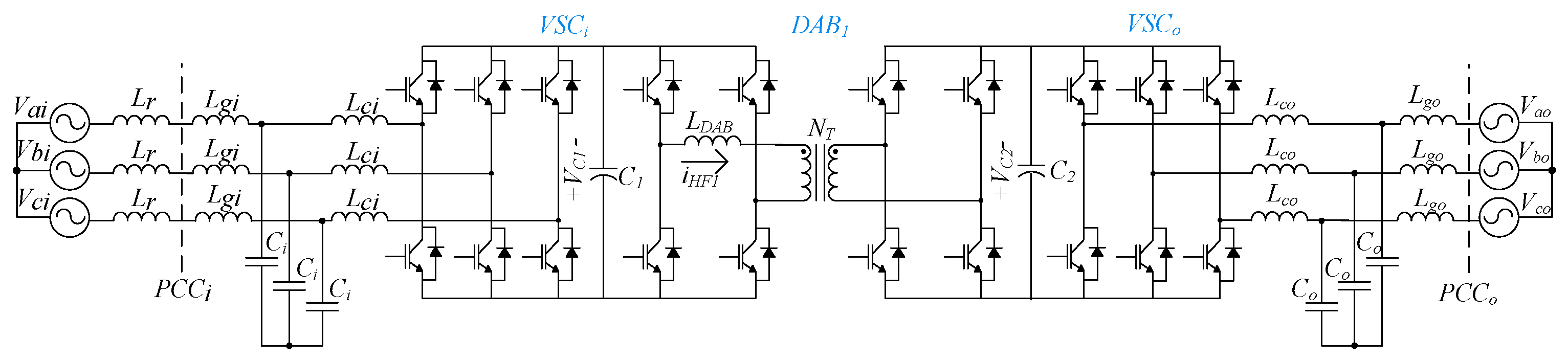
2. SST Topology
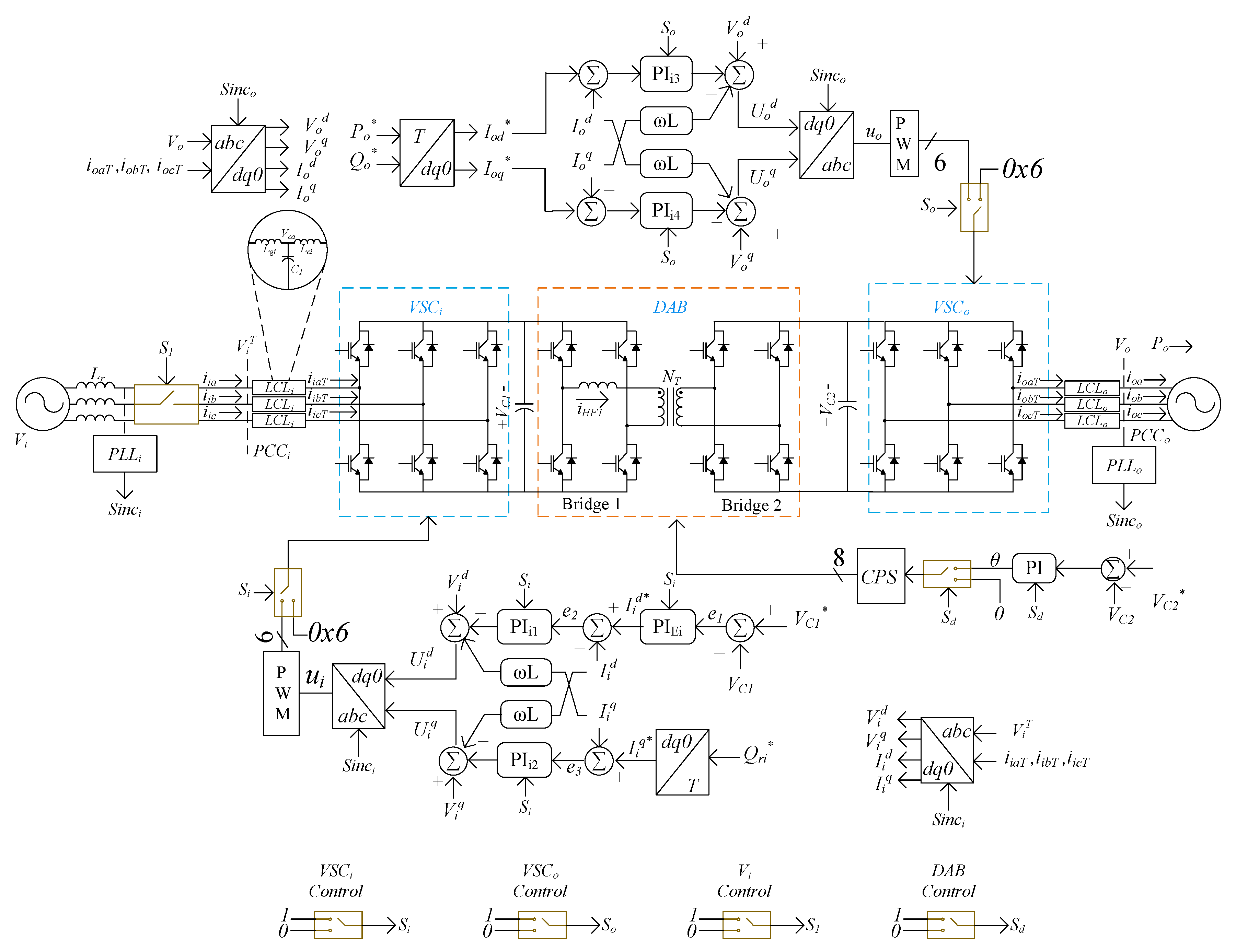
3. Control Strategy
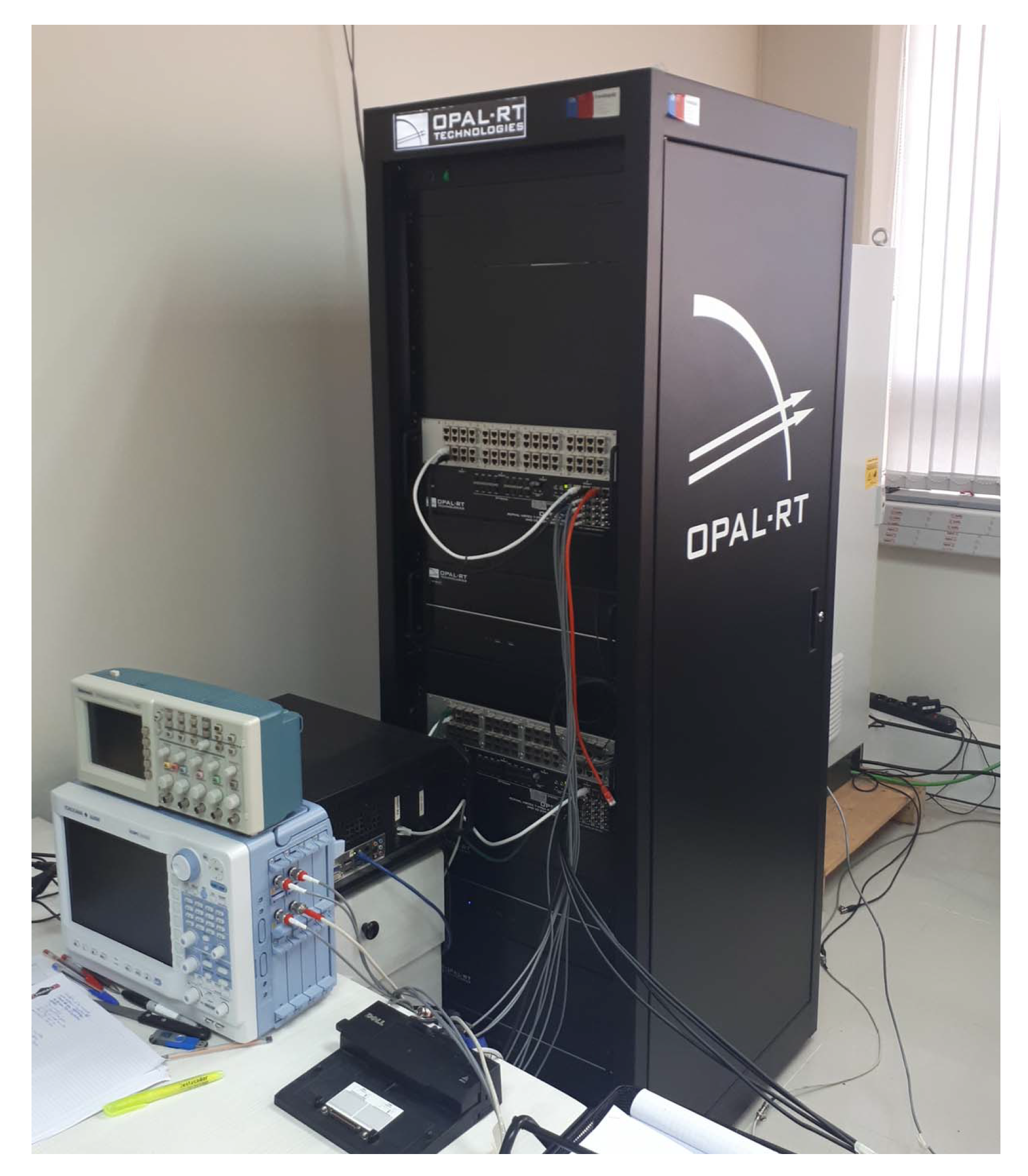
4. Digital Real-Time Simulator
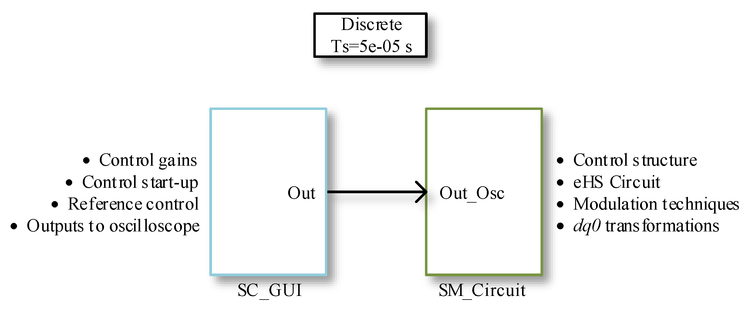
4.1. Simulation Circuit
4.2. eHS Circuit
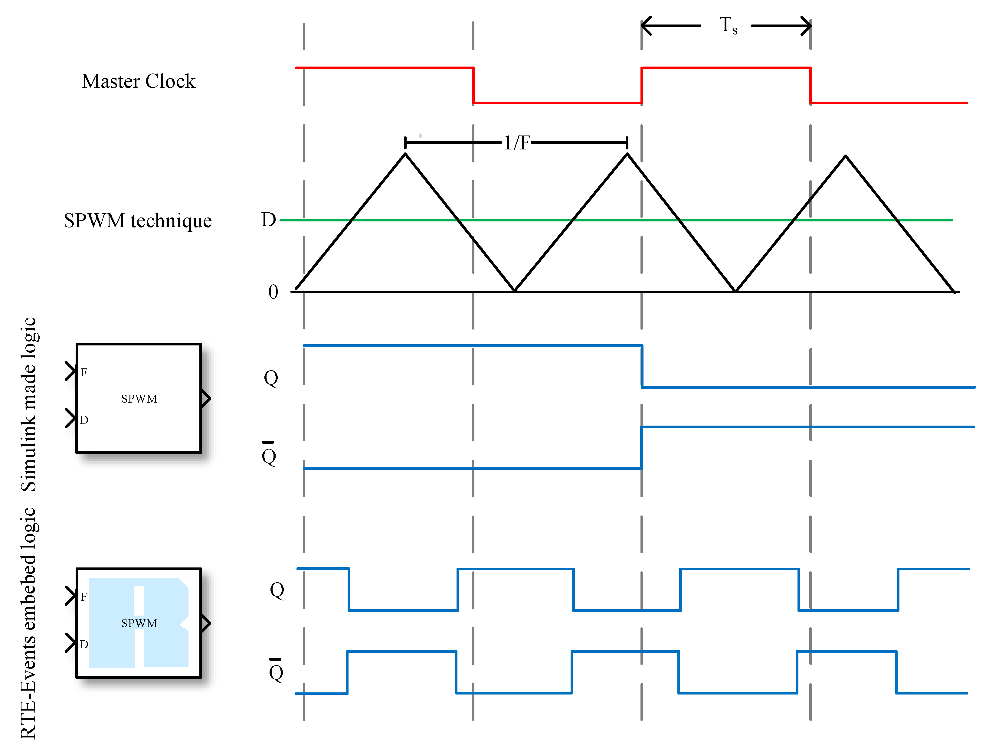
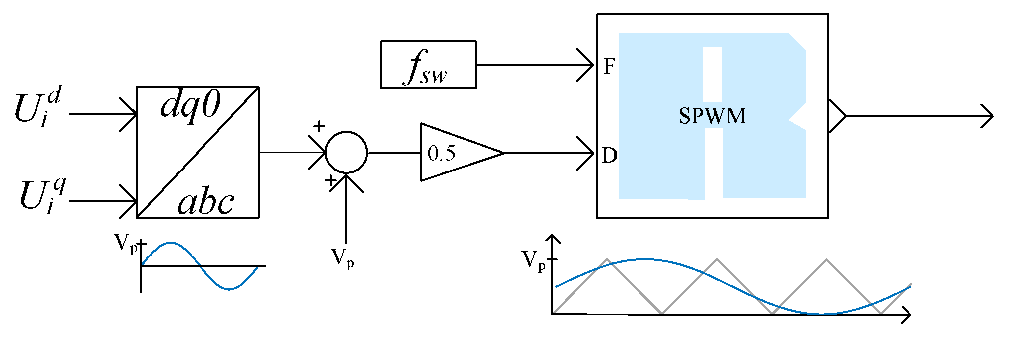
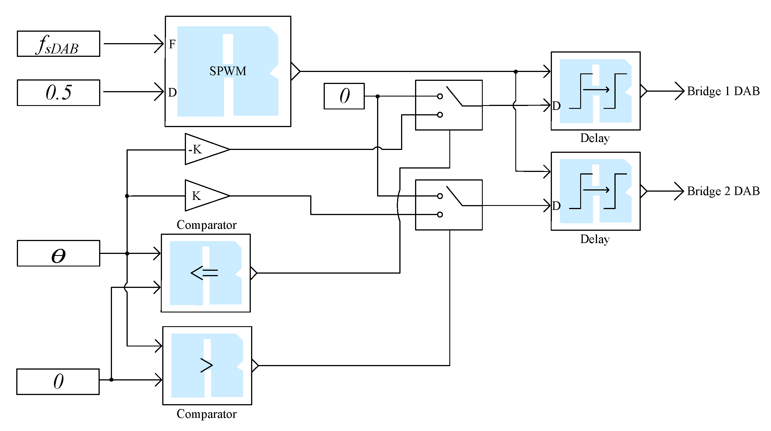
4.3. Modulation Schemes
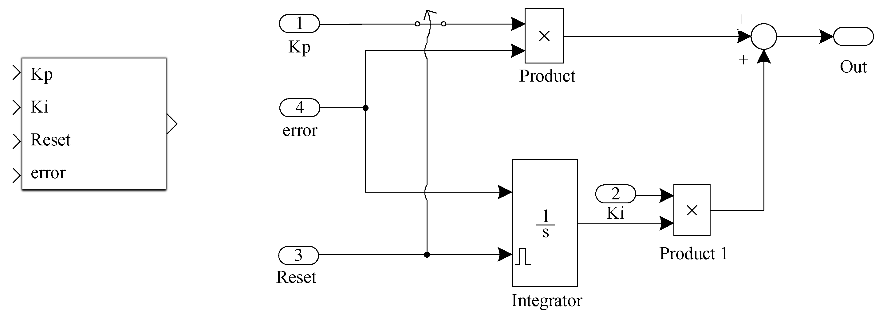
4.4. PI Controllers
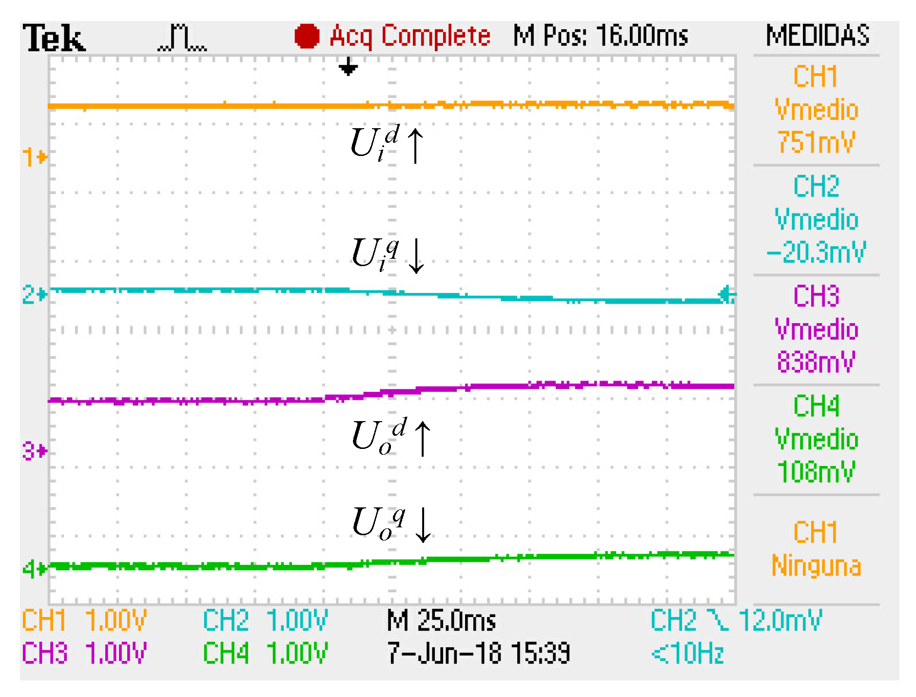
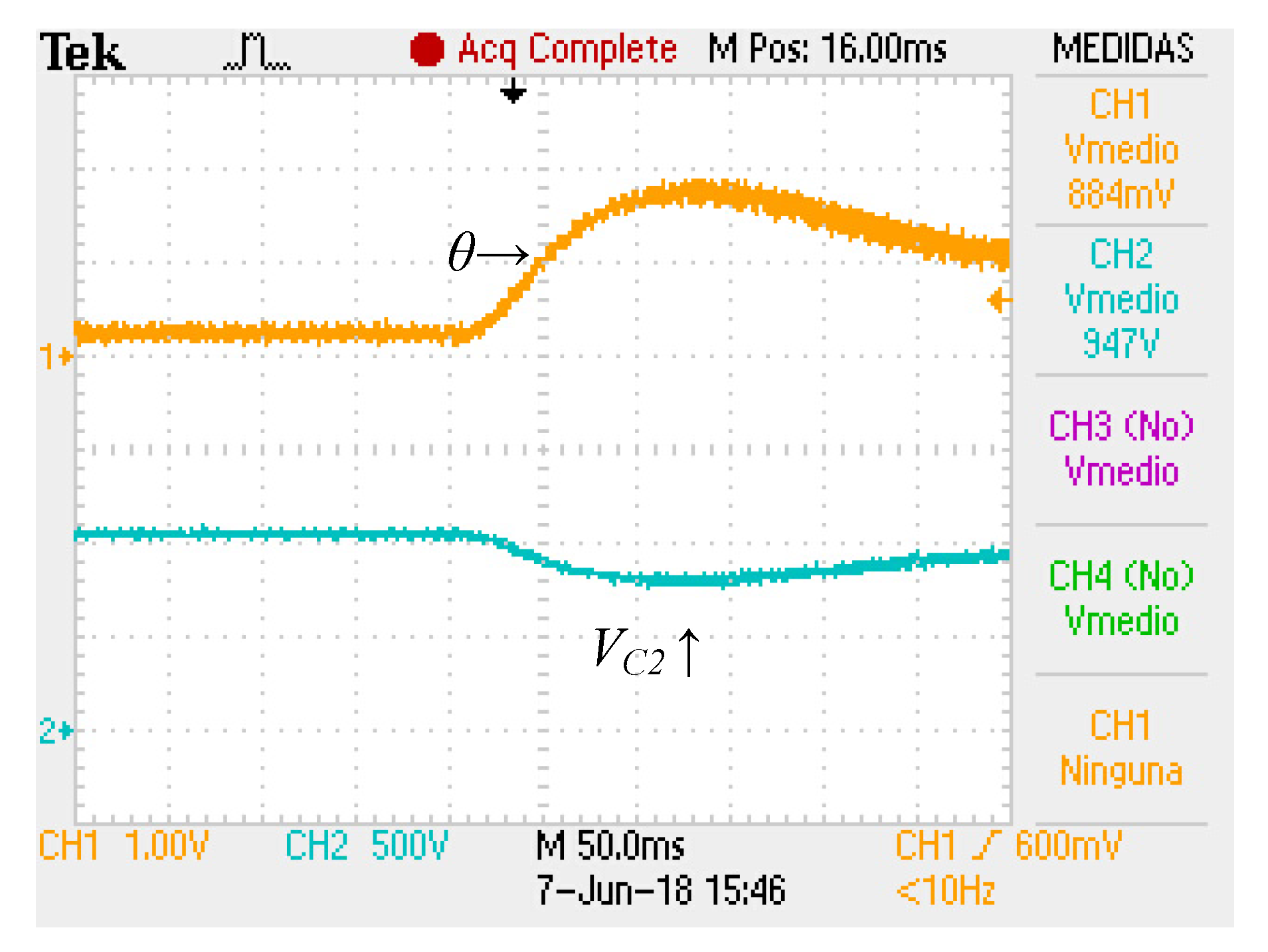
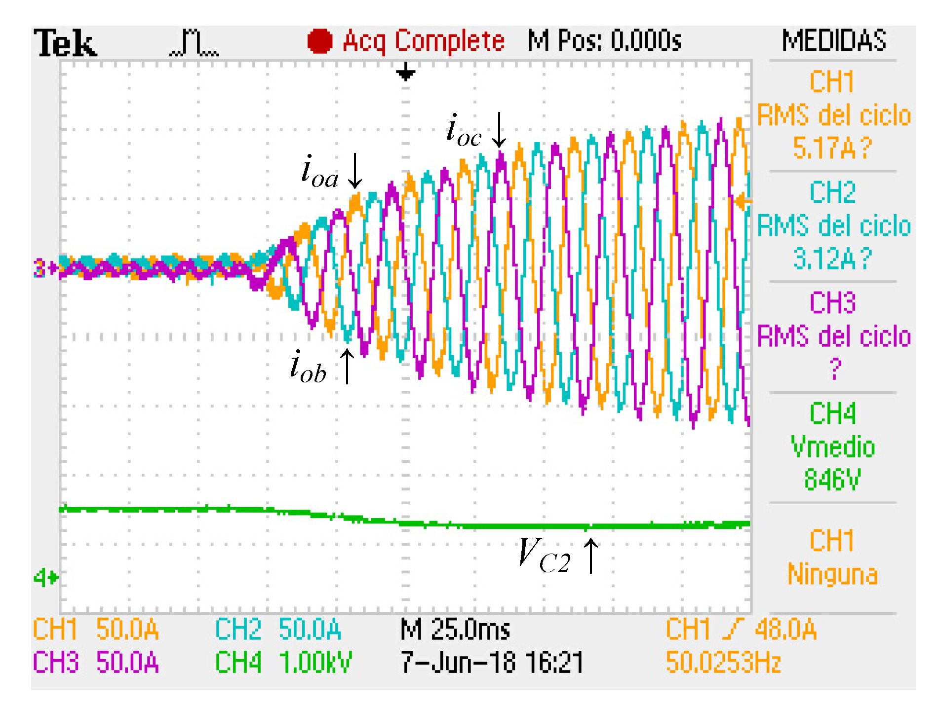
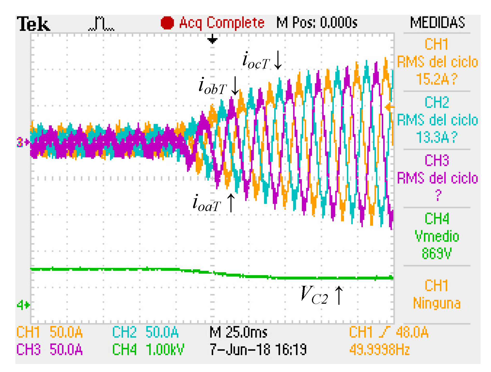
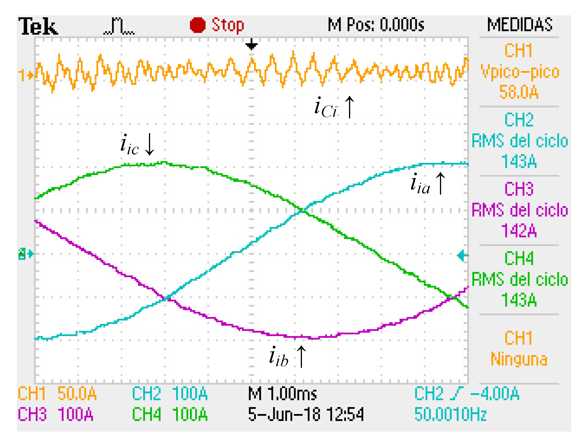
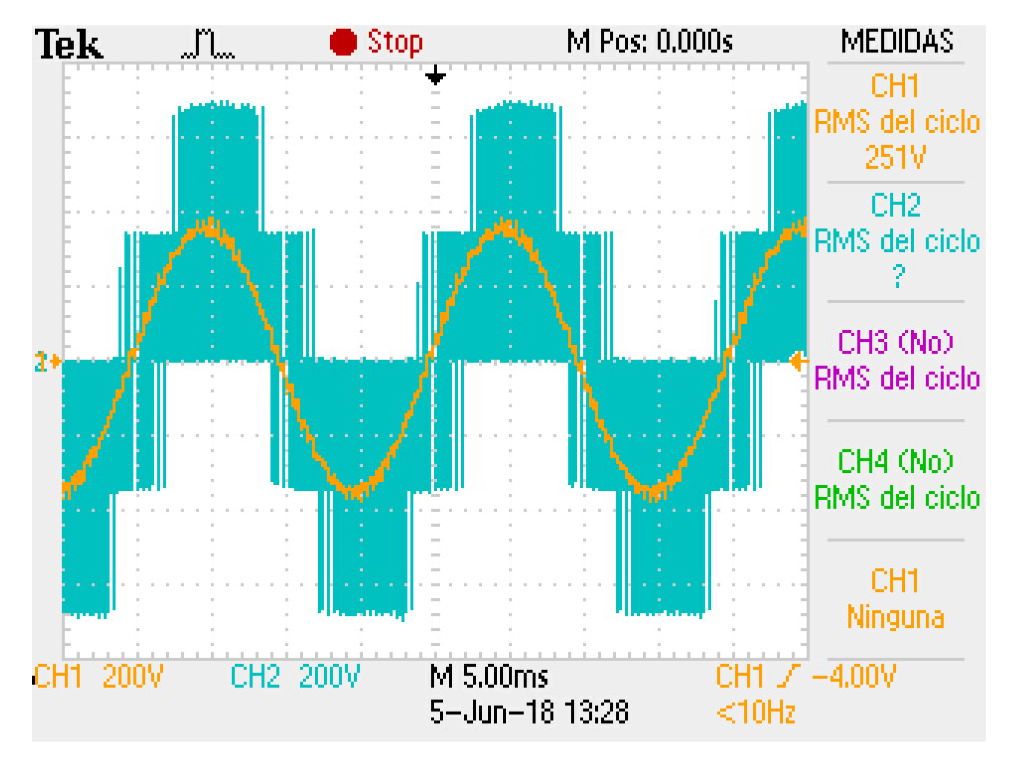
5. Real-Time Operation
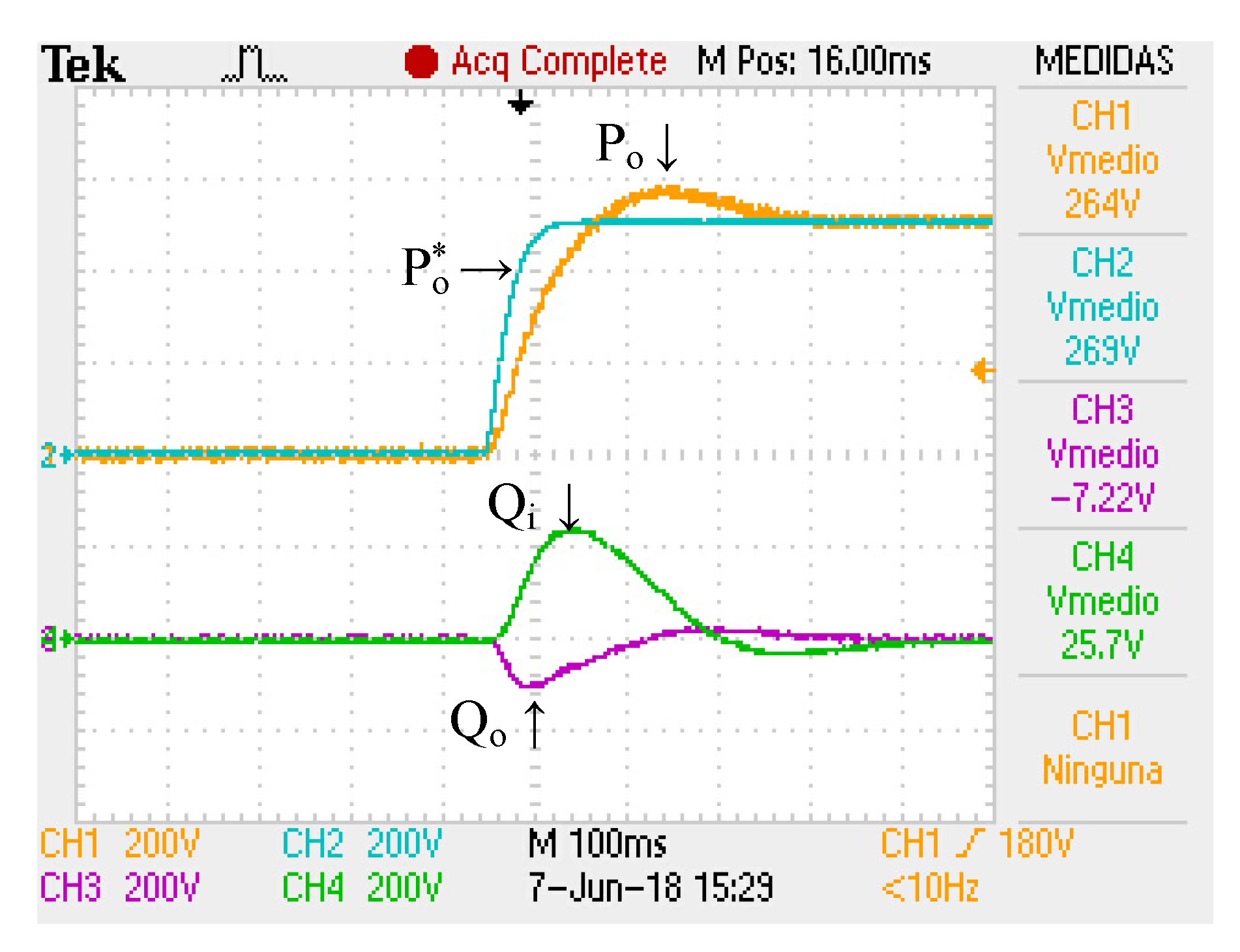
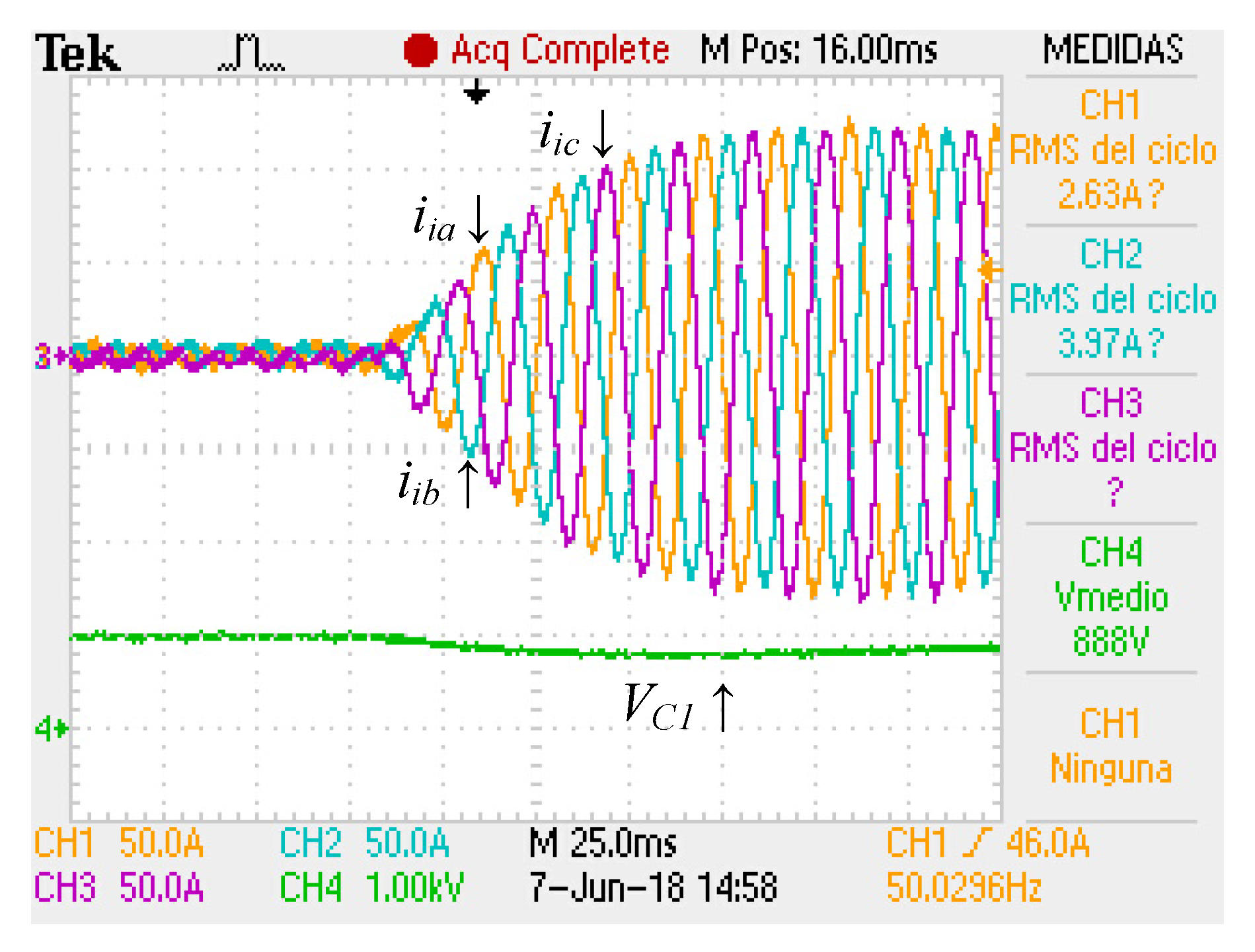
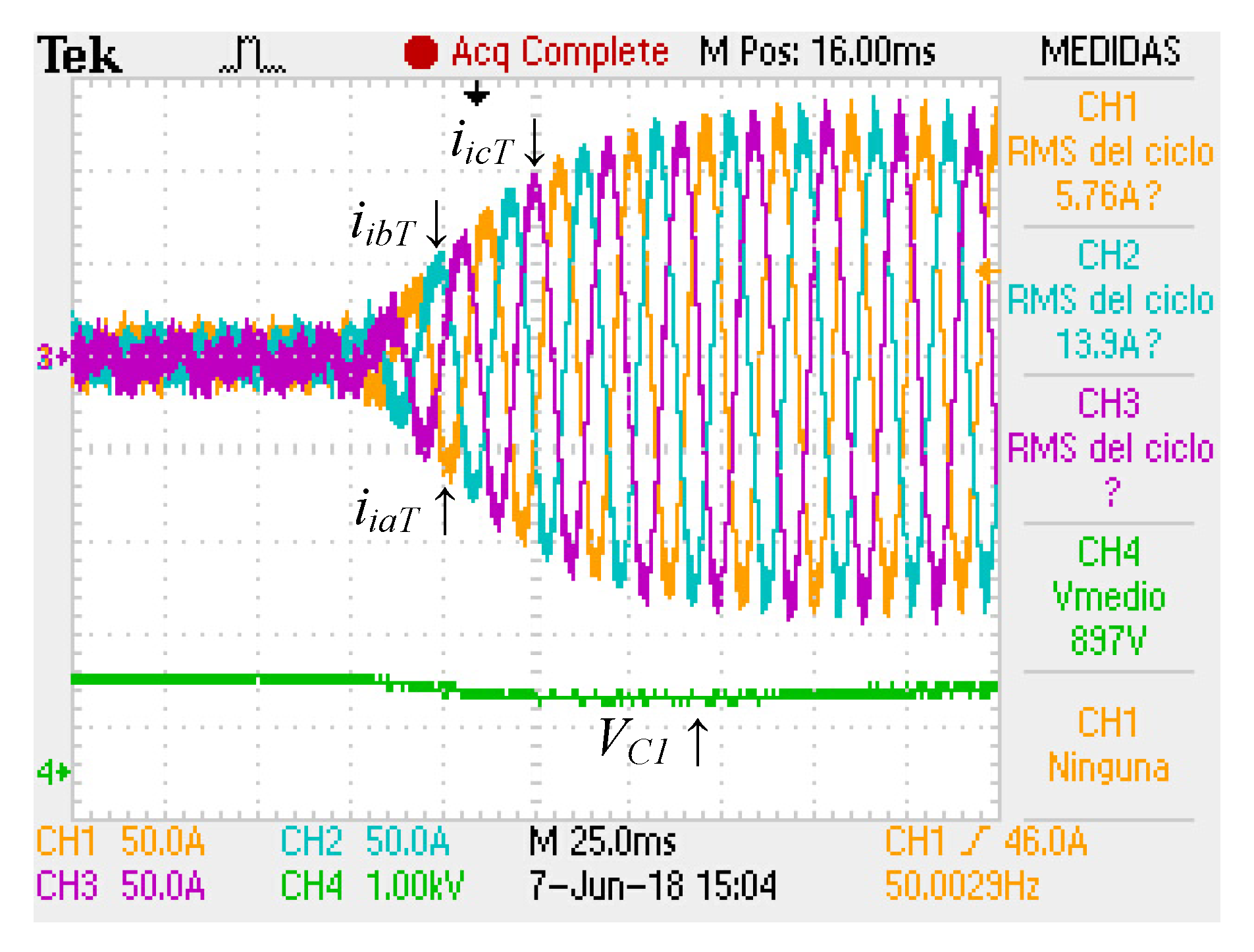
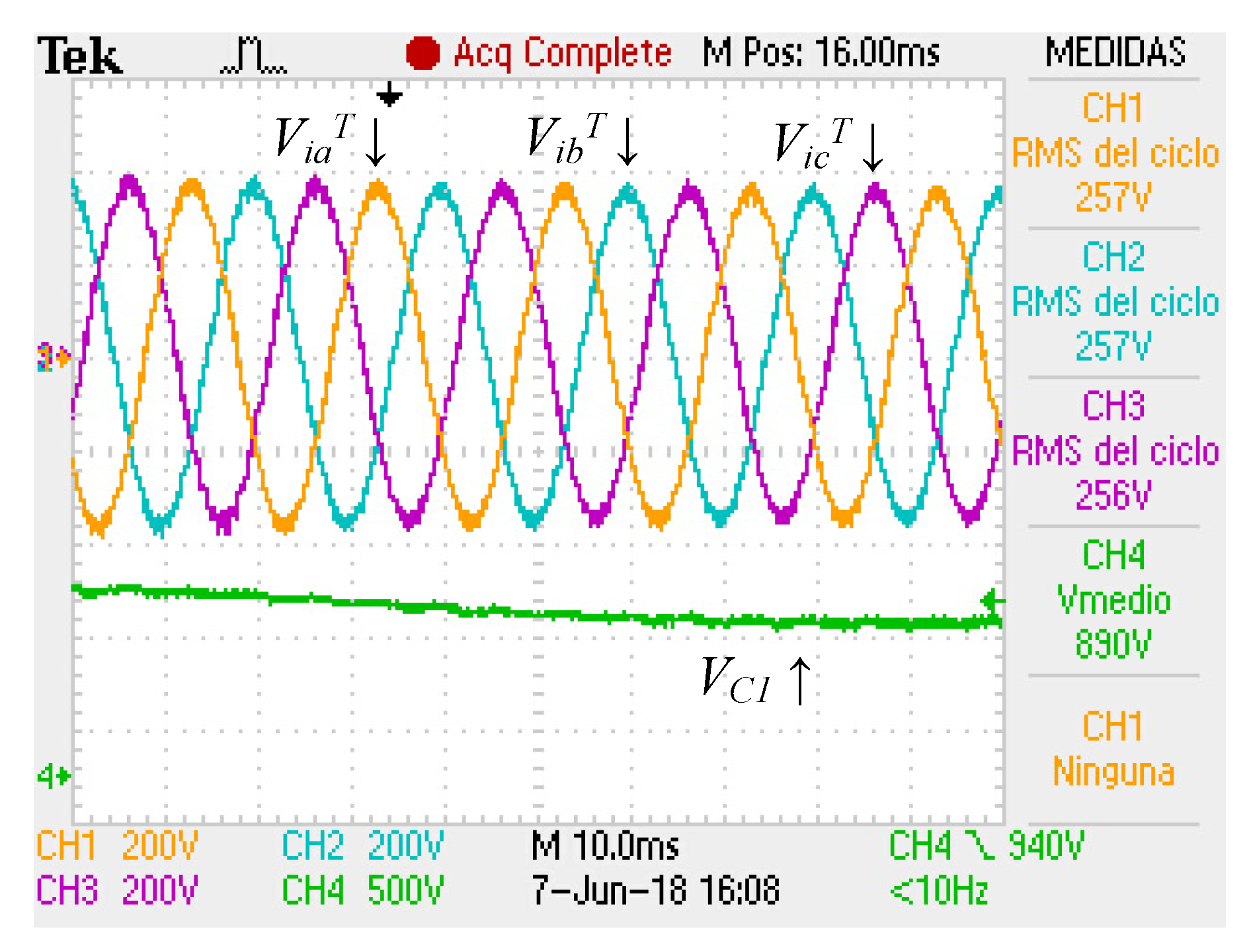
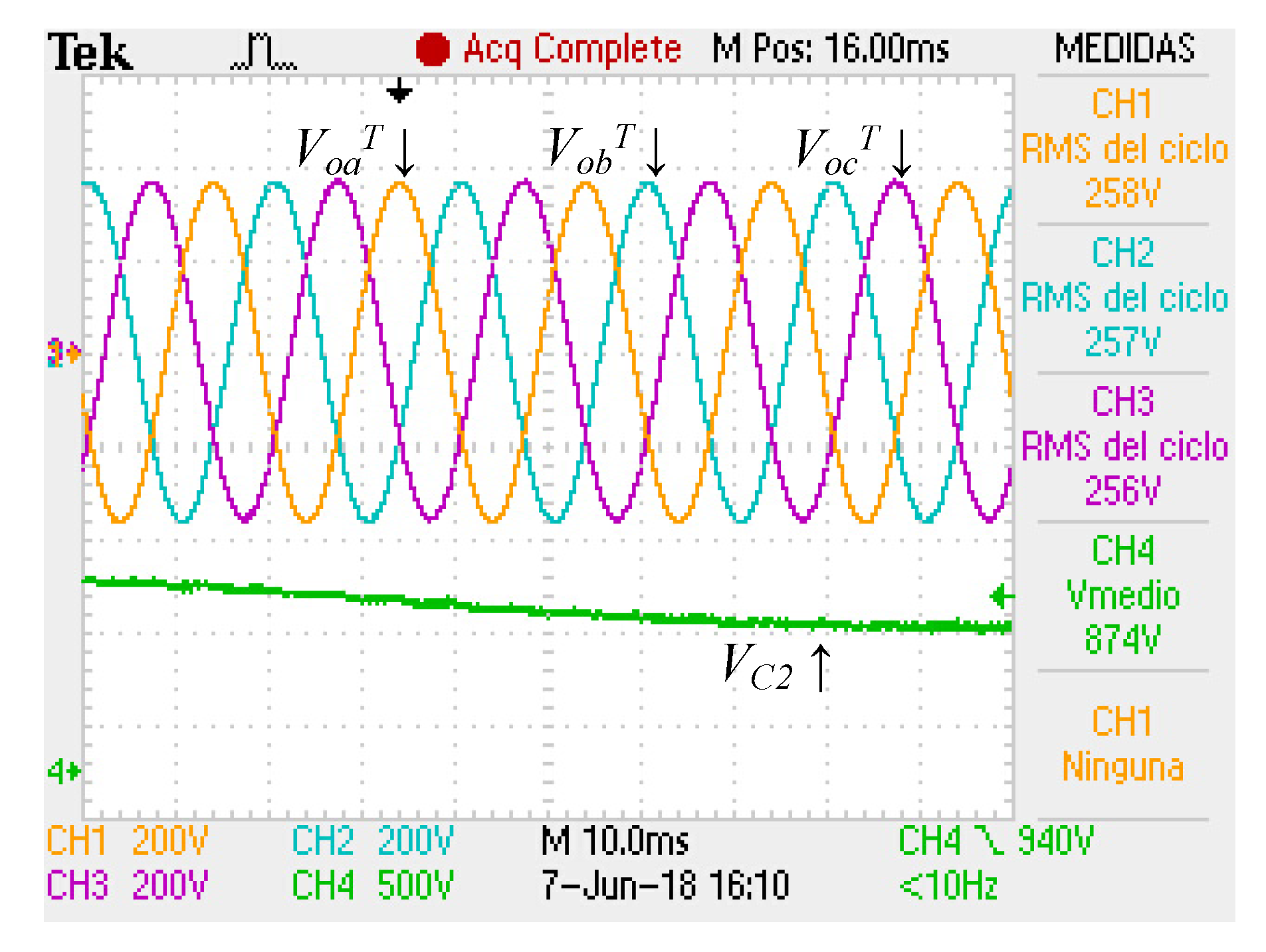
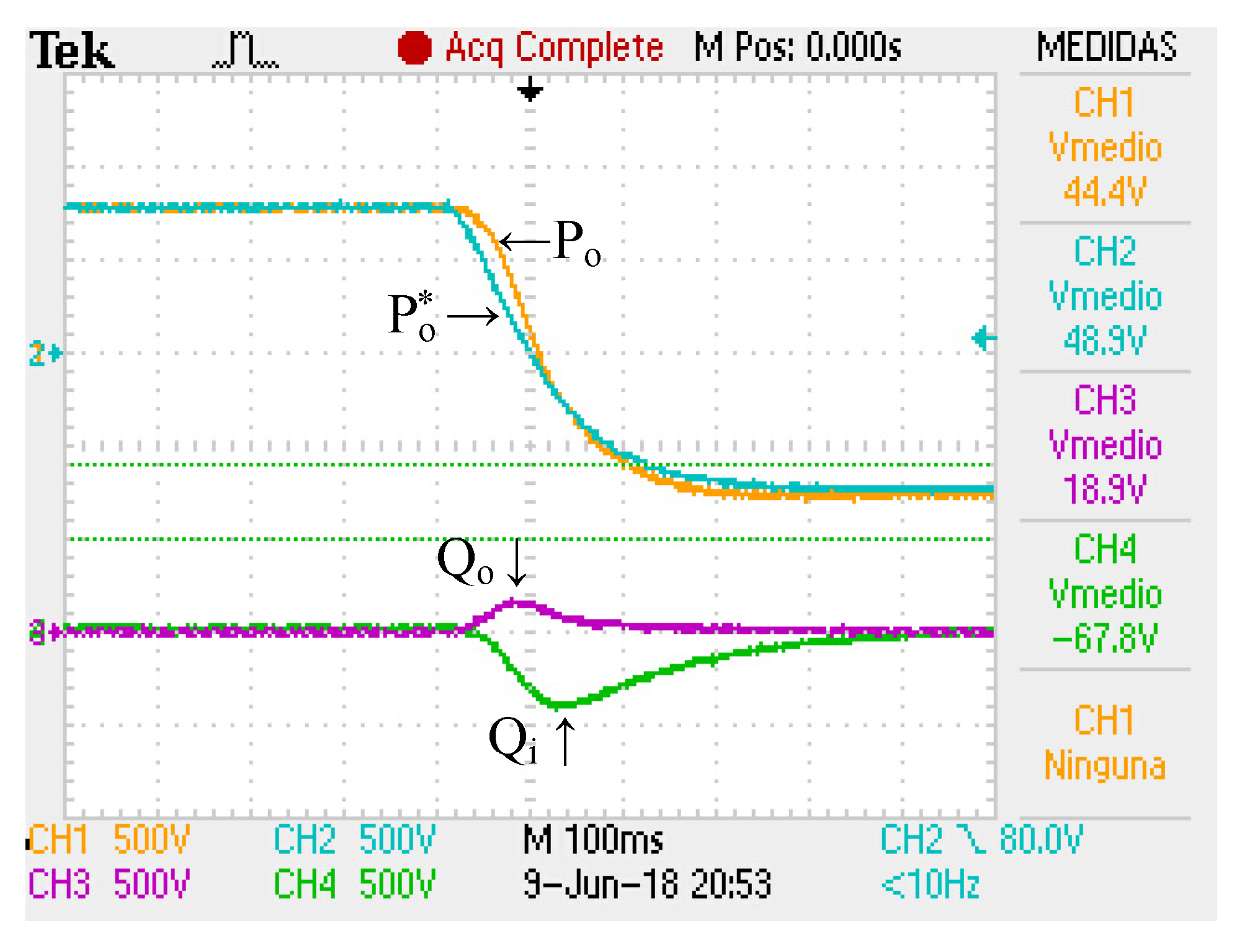
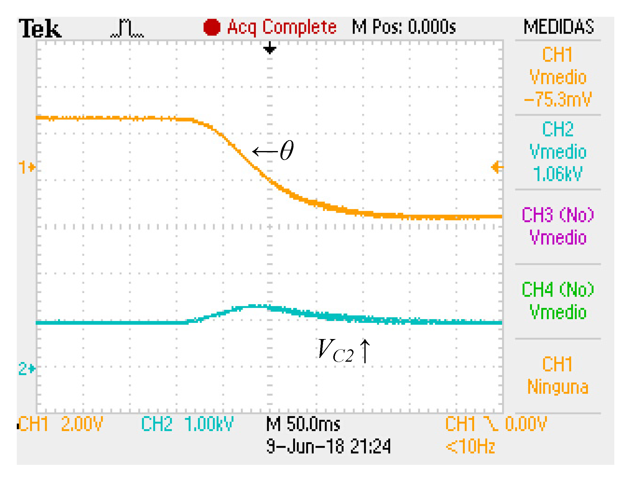
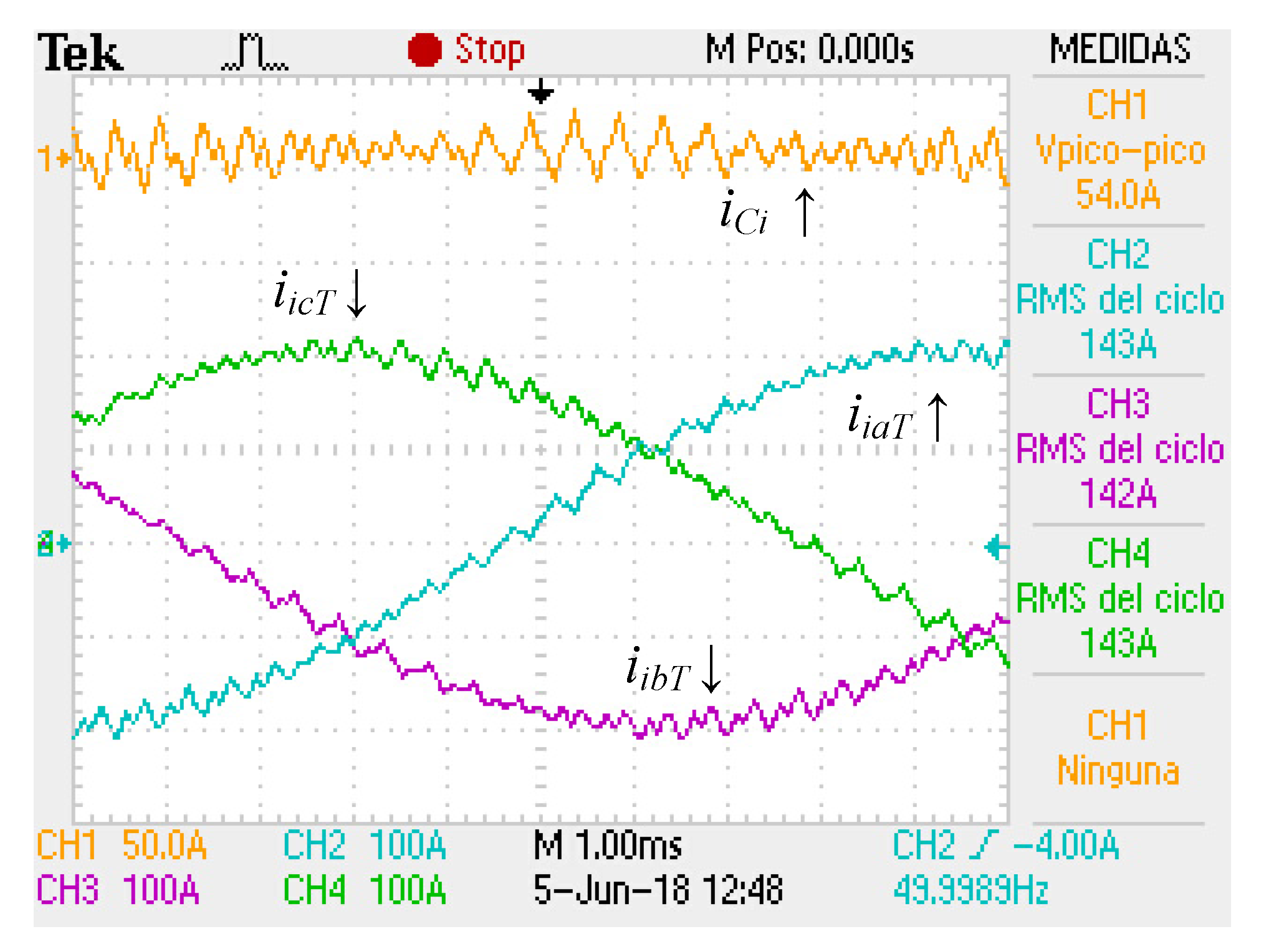
Simulation Results
6. Concluding Remarks
Author Contributions
Funding
Acknowledgments
Conflicts of Interest
References
- Bélanger, J.; Venne, P.; Paquin, J.N. The what, where, and why of real-time simulation. Planet RT 2010, 37–49. Available online: https://www.opal-rt.com/wp-content/themes/enfold-opal/pdf/L00161_0436.pdf (accessed on 23 February 2019).
- Kuffel, R.; Forsyth, P.; Peters, C. The Role and Importance of Real Time Digital Simulation in the Development and Testing of Power System Control and Protection Equipment. IFAC-PapersOnLine 2016, 49, 178–182. [Google Scholar] [CrossRef]
- Strasser, T. Real-Time Simulation Technologies for Power Systems Design, Testing, and Analysis. IEEE Power Energy Technol. Syst. J. 2015, 2, 63–73. [Google Scholar]
- She, X.; Yu, X.; Wang, F.; Huang, A.Q. Design and Demonstration of a 3.6-kV-120-V/10-kVA Solid-State Transformer for Smart Grid Application. IEEE Trans. Power Electron. 2014, 29, 3982–3996. [Google Scholar] [CrossRef]
- Pinto, S.F.; Mendes, P.V.; Silva, J.F. Modular Matrix Converter Based Solid State Transformer for smart grids. Electr. Power Syst. Res. 2016, 136, 189–200. [Google Scholar] [CrossRef]
- Huang, A.Q.; Crow, M.L.; Heydt, G.T.; Zheng, J.P.; Dale, S.J. The Future Renewable Electric Energy Delivery and Management (FREEDM) System: The Energy Internet. Proc. IEEE 2011, 99, 133–148. [Google Scholar] [CrossRef]
- Parreiras, T.; Machado, A.A.P.; Amaral, F.; Lobato, G.; Brito, J.A.S.; Cardoso, B. Forward Dual-Active-Bridge Solid State Transformer for a SiC-Based Cascaded Multilevel Converter Cell in Solar Applications. IEEE Trans. Ind. Appl. 2018, 54, 6353–6363. [Google Scholar] [CrossRef]
- Gao, R.; She, X.; Husain, I.; Huang, A.Q. Solid-State-Transformer-Interfaced Permanent Magnet Wind Turbine Distributed Generation System with Power Management Functions. IEEE Trans. Ind. Appl. 2017, 53, 3849–3861. [Google Scholar] [CrossRef]
- Syed, I.; Khadkikar, V. Replacing the Grid Interface Transformer in Wind Energy Conversion System with Solid-State Transformer. IEEE Trans. Power Syst. 2017, 32, 2152–2160. [Google Scholar] [CrossRef]
- Drabek, P.; Pittermann, M.; Los, M.; Bednar, B. Traction Drive with MFT-Novel Control Strategy Based on Zero Vectors Insertion. IFAC Proc. Vol. 2014, 47, 11968–11973. [Google Scholar] [CrossRef]
- Bednar, B.; Drabek, P.; Pittermann, M. The comparison of different variants of new traction drives with medium frequency transformer. In Proceedings of the 2016 International Symposium on Power Electronics, Electrical Drives, Automation and Motion (SPEEDAM), Anacapri, Italy, 22–24 June 2016; pp. 1172–1177. [Google Scholar] [CrossRef]
- Costa, L.F.; Carne, G.D.; Buticchi, G.; Liserre, M. The Smart Transformer: A solid-state transformer tailored to provide ancillary services to the distribution grid. IEEE Power Electron. Mag. 2017, 4, 56–67. [Google Scholar] [CrossRef]
- Milani, A.A.; Khan, M.T.A.; Chakrabortty, A.; Husain, I. Equilibrium Point Analysis and Power Sharing Methods for Distribution Systems Driven by Solid-State Transformers. IEEE Trans. Power Syst. 2018, 33, 1473–1483. [Google Scholar] [CrossRef]
- Martinez-Velasco, J.A.; Alepuz, S.; González-Molina, F.; Martin-Arnedo, J. Dynamic average modeling of a bidirectional solid state transformer for feasibility studies and real-time implementation. Electr. Power Syst. Res. 2014, 117, 143–153. [Google Scholar] [CrossRef]
- Jiang, Y.; Breazeale, L.; Ayyanar, R.; Mao, X. Simplified Solid State Transformer modeling for Real Time Digital Simulator (RTDS). In Proceedings of the 2012 IEEE Energy Conversion Congress and Exposition (ECCE), Raleigh, NC, USA, 15–20 September 2012; pp. 1447–1452. [Google Scholar] [CrossRef]
- Parma, G.G.; Dinavahi, V. Real-Time Digital Hardware Simulation of Power Electronics and Drives. IEEE Trans. Power Deliv. 2007, 22, 1235–1246. [Google Scholar] [CrossRef]
- Jack, A.G.; Atkinson, D.J.; Slater, H.J. Real-time emulation for power equipment development. I. Real-time simulation. IEEE Proc. Electr. Power Appl. 1998, 145, 92–97. [Google Scholar] [CrossRef]
- Peña-Alzola, R.; Blaabjerg, F. Chapter 8—Design and Control of Voltage Source Converters with LCL-Filters. In Control of Power Electronic Converters and Systems; Blaabjerg, F., Ed.; Academic Press: Cambridge, MA, USA, 2018; pp. 207–242. [Google Scholar]
- Opal-RT Training Services. RT-LAB Solution for Real-Time Applications, OP101: Getting Started; Opal-RT Technologies Inc.: Montréal, QC, Canada, 2013. [Google Scholar]
- Pejovic, P.; Maksimovic, D. A new algorithm for simulation of power electronic systems using piecewise-linear device models. IEEE Trans. Power Electron. 1995, 10, 340–348. [Google Scholar] [CrossRef]
- Opal-RT. eHS User Guide; Opal-RT Technologies Inc.: Montréal, QC, Canada, 2017. [Google Scholar]
- McLyman, C. Transformer and Inductor Design Handbook; CRC Press: Boca Raton, FL, USA, 2017. [Google Scholar]
- Vadhiraj, S.; Swamy, K.N.; Divakar, B.P. Generic SPWM technique for multilevel inverter. In Proceedings of the 2013 IEEE PES Asia-Pacific Power and Energy Engineering Conference (APPEEC), Kowloon, China, 8–11 December 2013; pp. 1–5. [Google Scholar] [CrossRef]


| Parameter | Symbol | Value | Units | |
|---|---|---|---|---|
| Grid | Short-circuit power | 10 | MVA | |
| Grid inductance | 60.4 | H | ||
| Voltage 3 | 220 | V | ||
| Voltage 3 | 220 | V | ||
| Grid frequency | 50 | Hz | ||
| LCL Filter | LCL converter side inductor | 150 | H | |
| Operating VARS 3 for | 240 | kVAR | ||
| LCL grid side inductor | 15 | H | ||
| Operating VARs 3 for | 243 | kVAR | ||
| LCL Capacitor | 432 | F | ||
| Complete operating VARs | 243.1 | kVAR | ||
| Frequencies | Resonance frequency | 875 | Hz | |
| Resonance frequency | 1.075 | kHz | ||
| Outer loop bandwidth | 35 | Hz | ||
| Inner loop bandwidth | 450 | Hz | ||
| Converter | Total apparent power | 1.02 | MVA | |
| Capacitor | 2600 | F | ||
| Link inductor | 0.005 | mH | ||
| Capacitor | 1200 | F | ||
| Switching frequency | 2.15 | kHz | ||
| DAB Switching frequency | 5 | kHz | ||
| DC voltages | 1000 | V |
| Parameter | Value |
|---|---|
| Number of Inputs | 32 |
| Number of Outputs | 32 |
| Number of Switches | 64 |
| Maximum number of states | 150 |
| Calculation power | 25.6 GFLOPS |
| Solving time | ≈200 nS |
| Parameter | Time [s] | [%] |
|---|---|---|
| Data acquisition | 0.08 | 0.16 |
| Major computation time | 13.24 | 26.48 |
| Minor computation time | 0.18 | 0.36 |
| Opctrl recv (EHS) | 0.1 | 0.2 |
| Execution cycle | 14.29 | 28.57 |
© 2019 by the authors. Licensee MDPI, Basel, Switzerland. This article is an open access article distributed under the terms and conditions of the Creative Commons Attribution (CC BY) license (http://creativecommons.org/licenses/by/4.0/).
Share and Cite
Almaguer, J.; Cárdenas, V.; Espinoza, J.; Aganza-Torres, A.; González, M. Performance and Control Strategy of Real-Time Simulation of a Three-Phase Solid-State Transformer. Appl. Sci. 2019, 9, 789. https://doi.org/10.3390/app9040789
Almaguer J, Cárdenas V, Espinoza J, Aganza-Torres A, González M. Performance and Control Strategy of Real-Time Simulation of a Three-Phase Solid-State Transformer. Applied Sciences. 2019; 9(4):789. https://doi.org/10.3390/app9040789
Chicago/Turabian StyleAlmaguer, Jorge, Víctor Cárdenas, Jose Espinoza, Alejandro Aganza-Torres, and Marcos González. 2019. "Performance and Control Strategy of Real-Time Simulation of a Three-Phase Solid-State Transformer" Applied Sciences 9, no. 4: 789. https://doi.org/10.3390/app9040789
APA StyleAlmaguer, J., Cárdenas, V., Espinoza, J., Aganza-Torres, A., & González, M. (2019). Performance and Control Strategy of Real-Time Simulation of a Three-Phase Solid-State Transformer. Applied Sciences, 9(4), 789. https://doi.org/10.3390/app9040789