Recent Progress on Irradiation-Induced Defect Engineering of Two-Dimensional 2H-MoS2 Few Layers

 ,
,  ,
, 


Abstract
1. Introduction
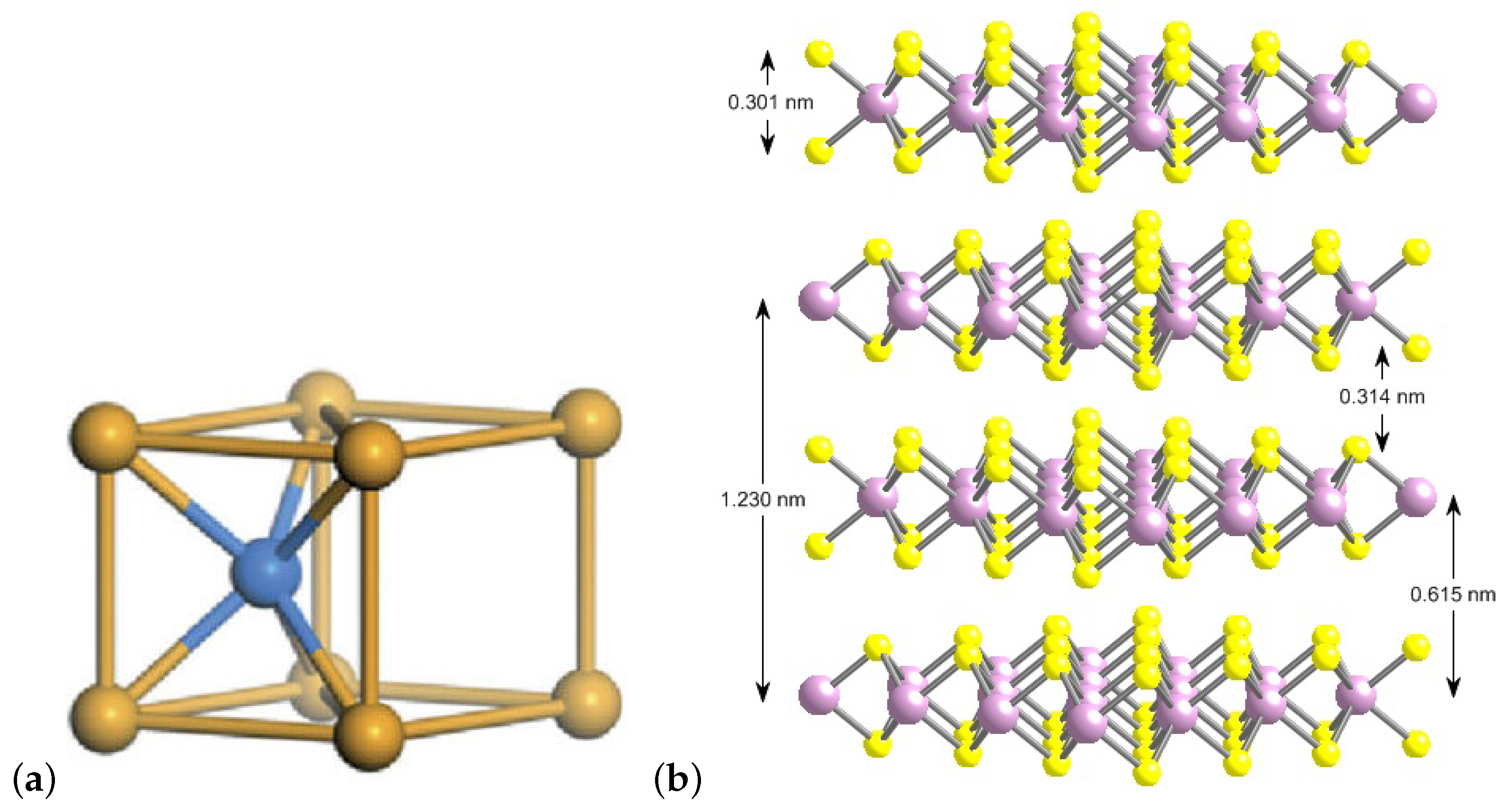
1.1. MoS 2D Materials
1.2. Irradiation Sources
1.3. Irradiated MoS Materials
2. Charged Particle Irradiation
2.1. Swift-Heavy Ion Irradiation
2.1.1. Uranium-238 Ion Irradiation
2.1.2. Gallium Ion Irradiation
2.1.3. Xenon Ion Irradiation
2.1.4. Bismuth Ion Irradiation
2.1.5. Manganese Ion Irradiation
2.1.6. Gold Ion Irradiation
2.1.7. Silver Ion Irradiation
2.1.8. C Ion Irradiation
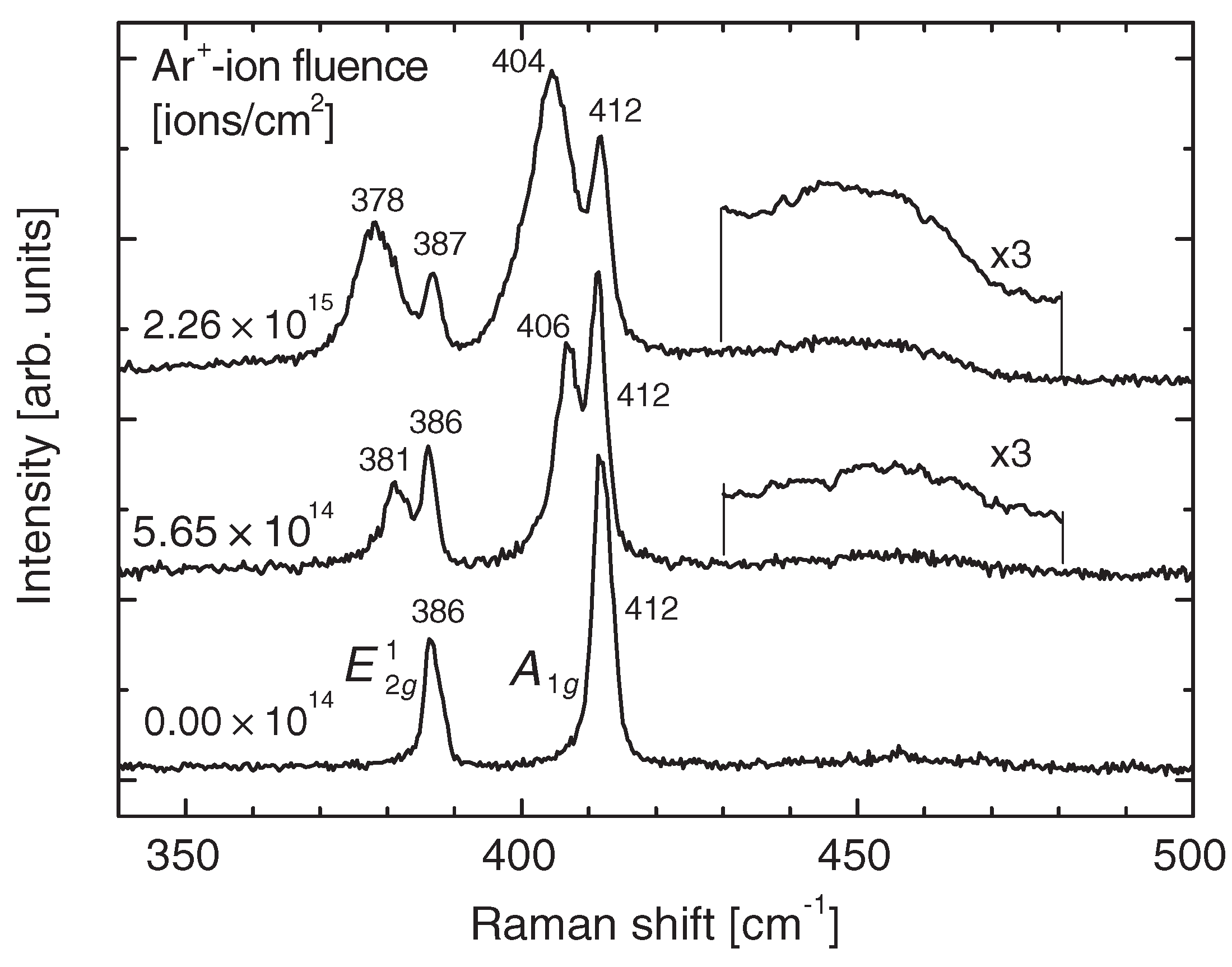
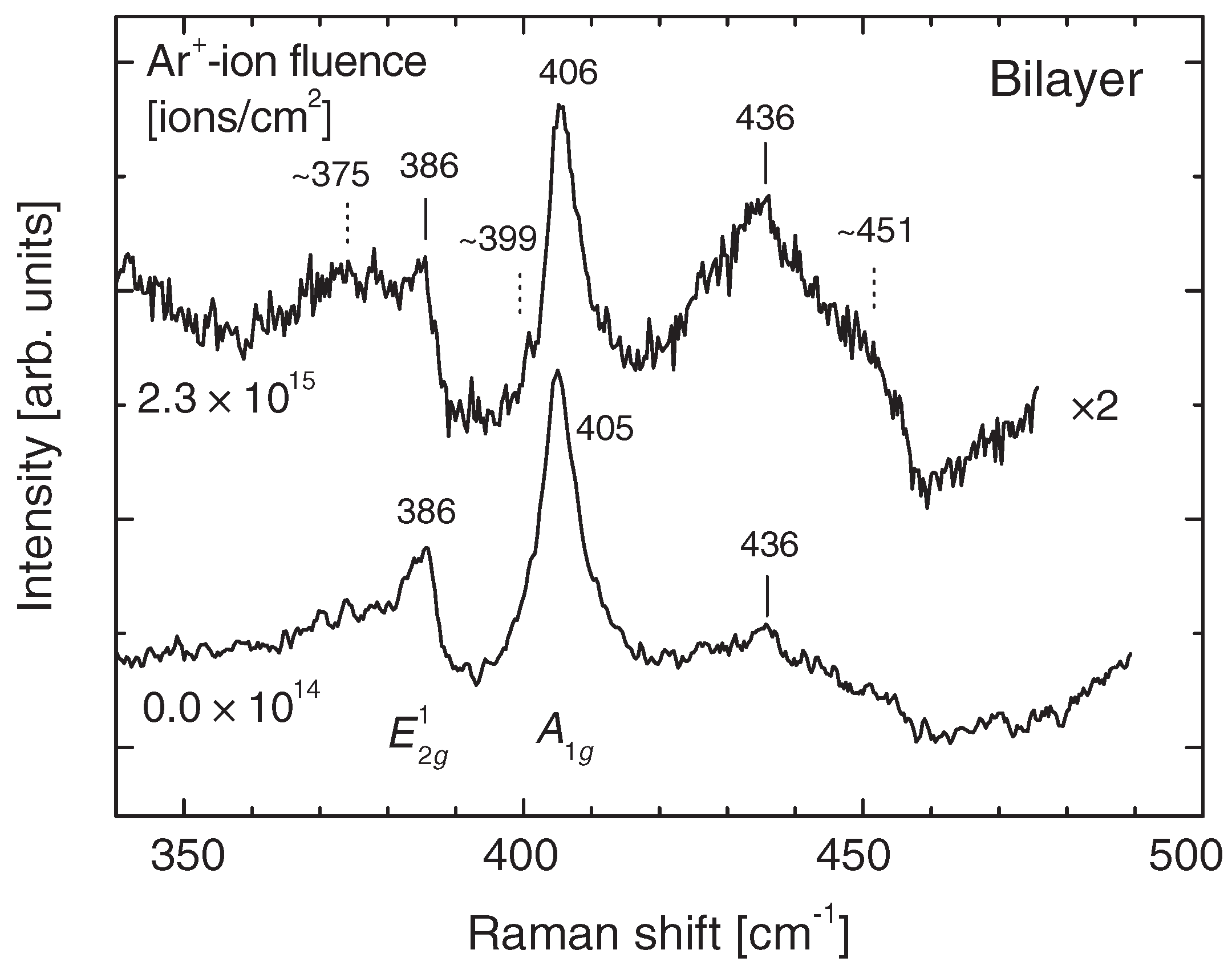
2.2. Argon Ion Irradiation
2.3. Neon Ion Irradiation
2.4. Alpha-Particle/Helium-Ion Irradiation
2.5. Proton Irradiation
2.6. Electron Irradiation
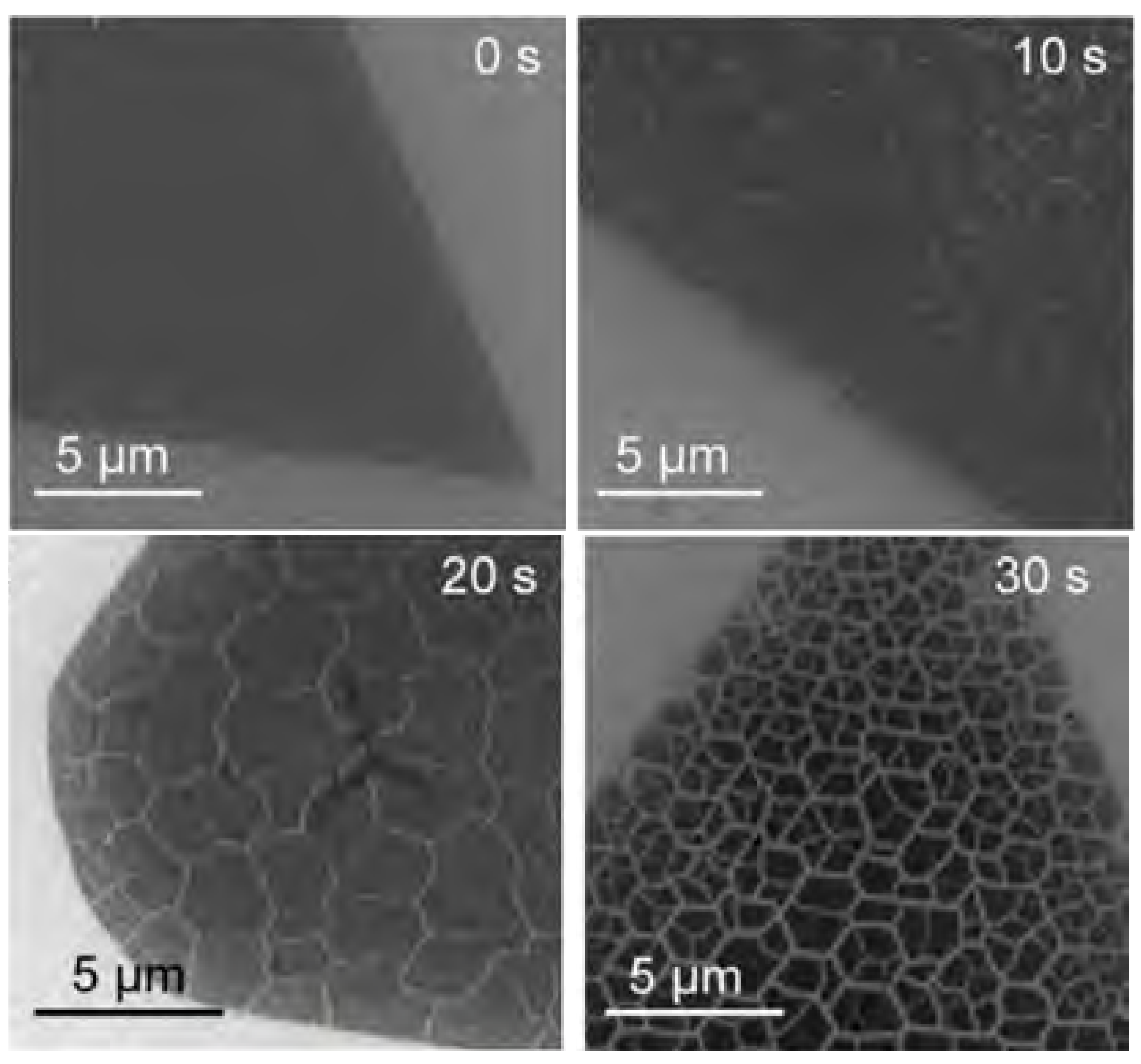
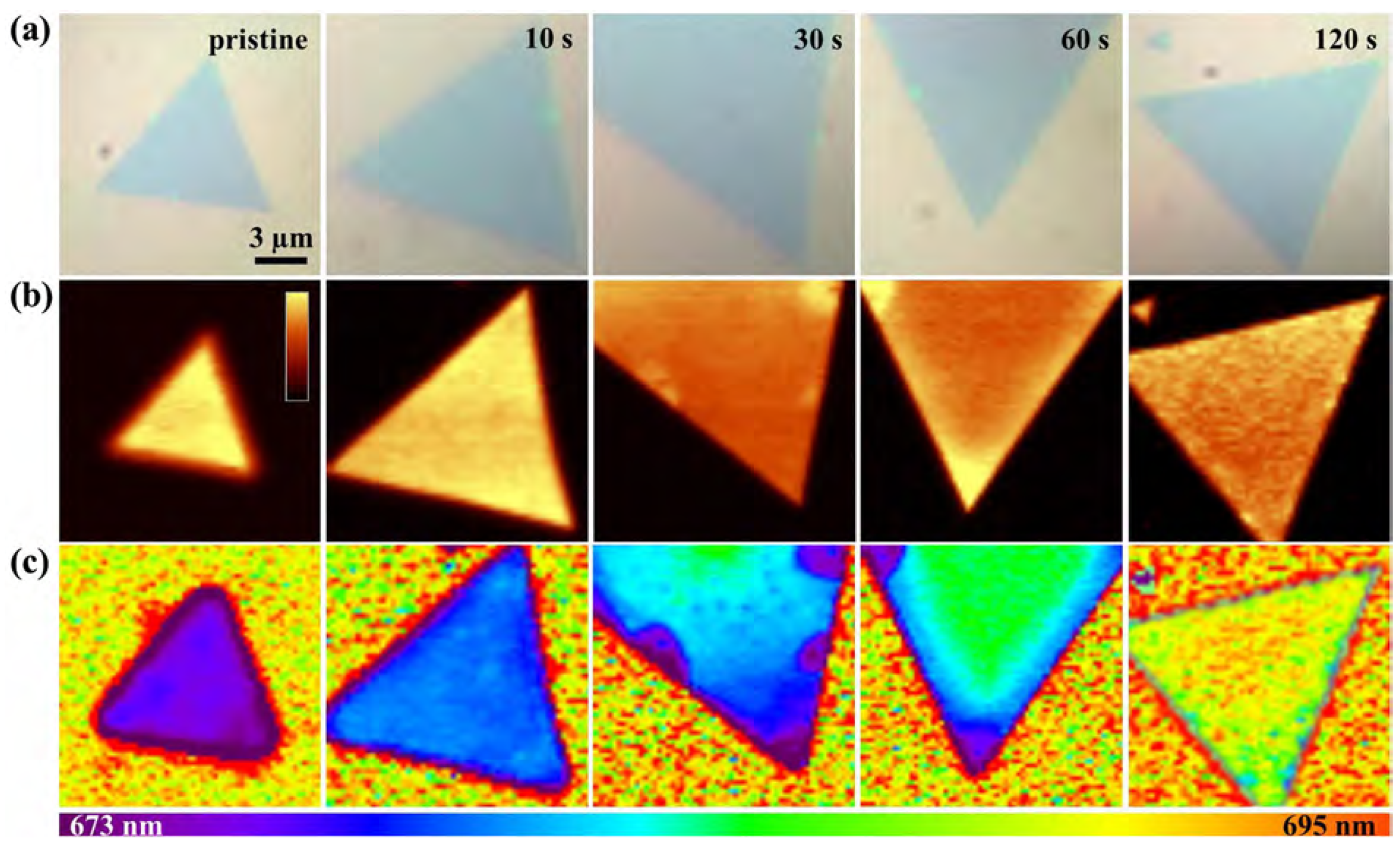
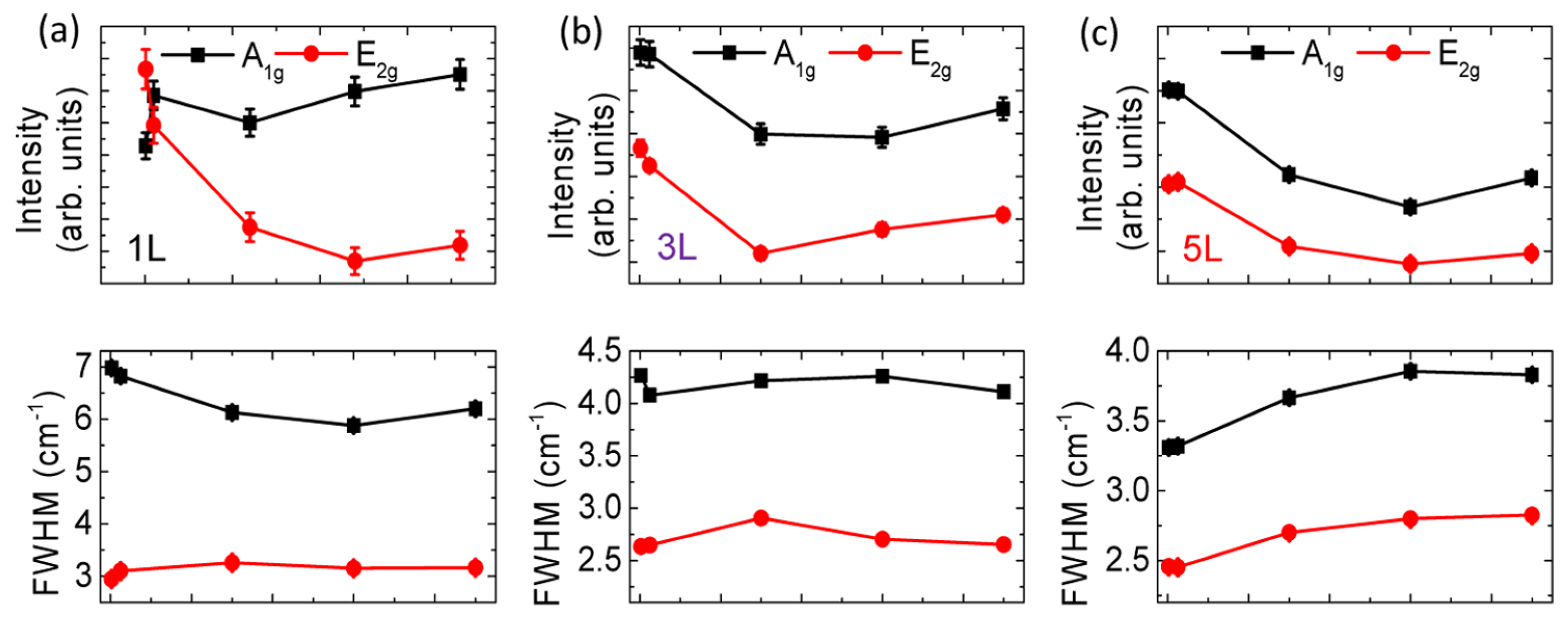
2.7. Plasma Irradiation
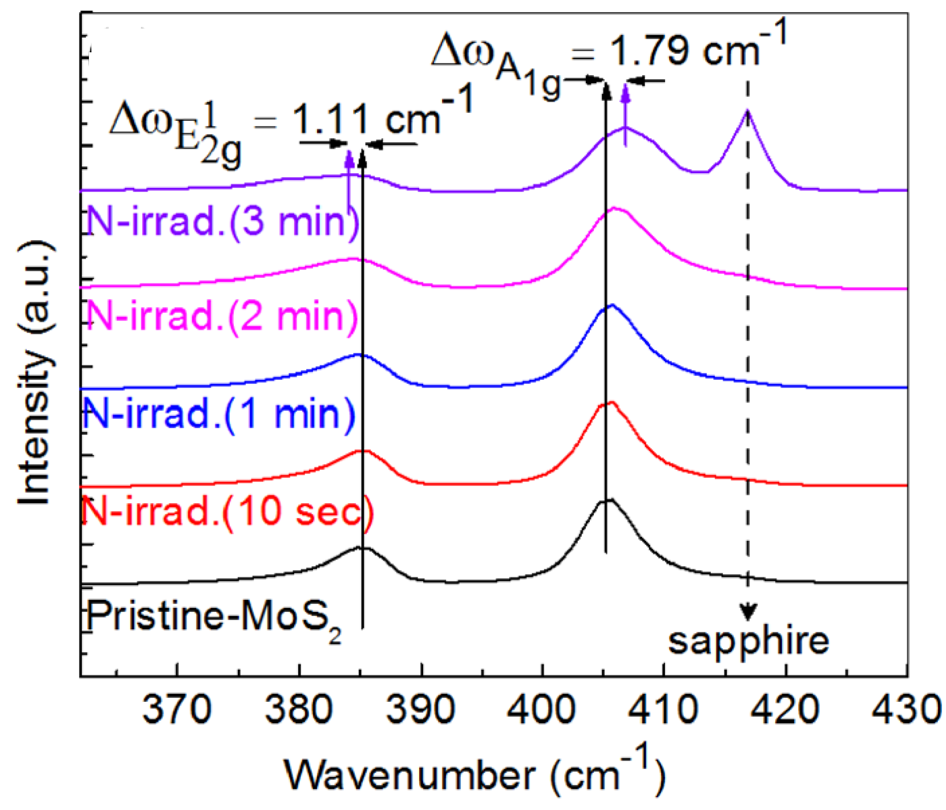
2.7.1. Active Nitrogen N
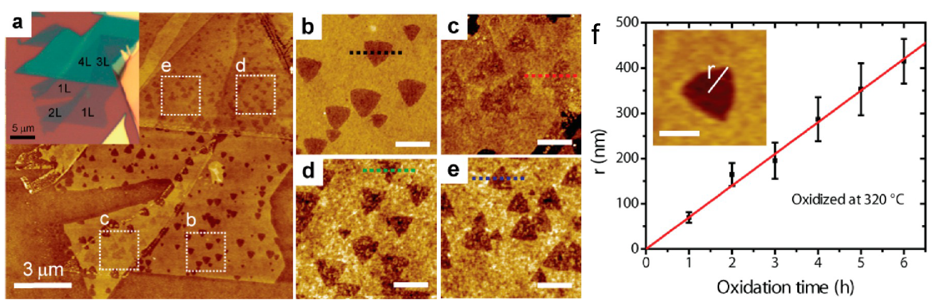
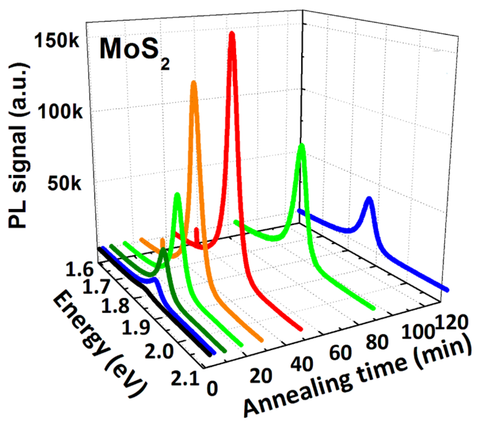
2.7.2. Active Oxygen O
2.7.3. Active Hydrogen H
2.7.4. Other Molecules
Fluoride
Chlorine
Phosphorus
Gallium
Combination
3. Electromagnetic Irradiation
3.1. Gamma-ray Irradiation
3.2. X-ray Irradiation
3.3. Ultraviolet Light Irradiation
3.4. Visible Light Irradiation
3.5. Infrared Light Irradiation
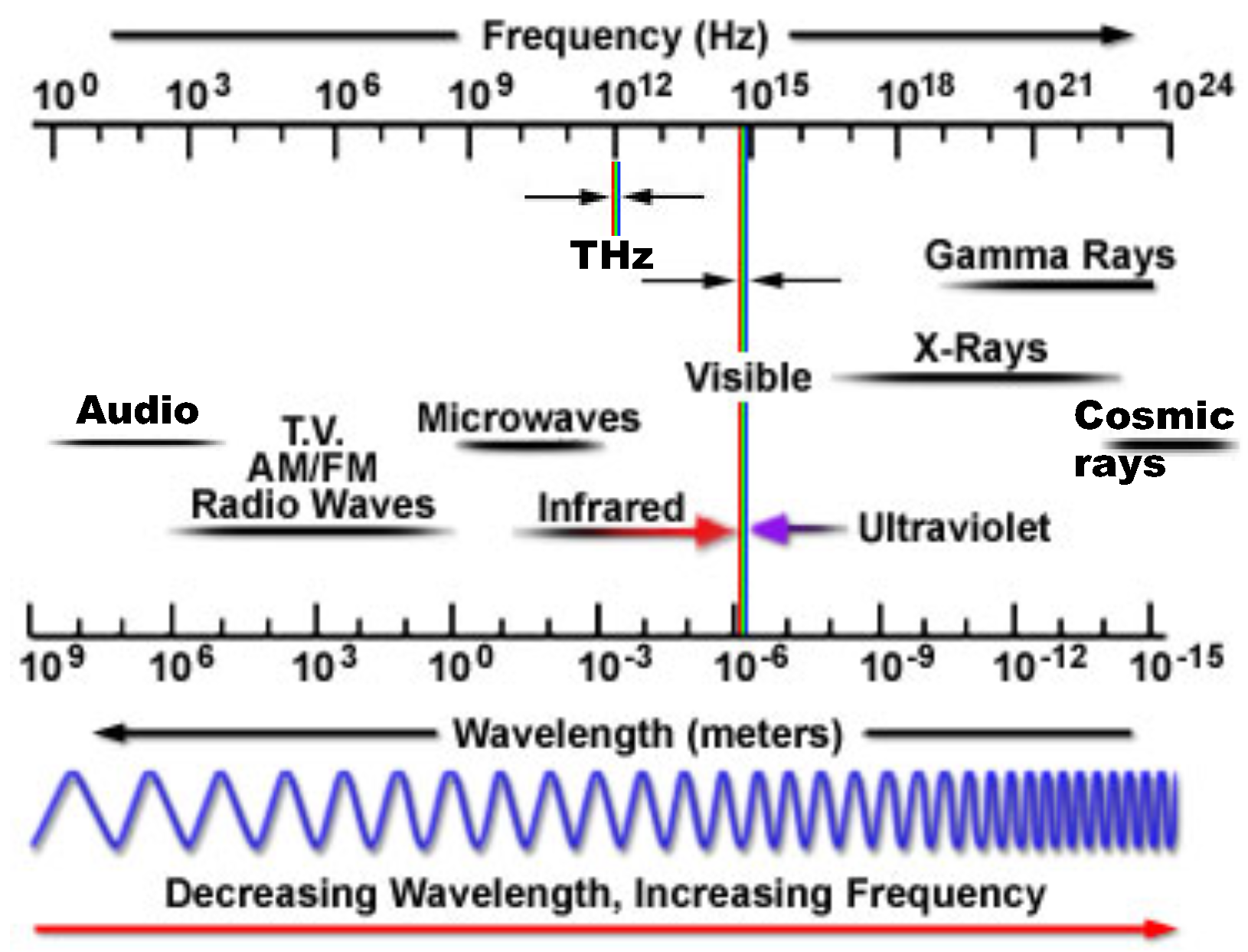
3.6. Terahertz Wave Irradiation
3.7. Microwave Irradiation
4. Other Irradiation
4.1. Ultrasonic Wave Irradiation
4.2. Thermal Irradiation
4.3. Hybrid Irradiation: UV–Ozone Treatments
5. Irradiation Mechanism and Theoretical Simulations
6. Irradiation-Induced Properties
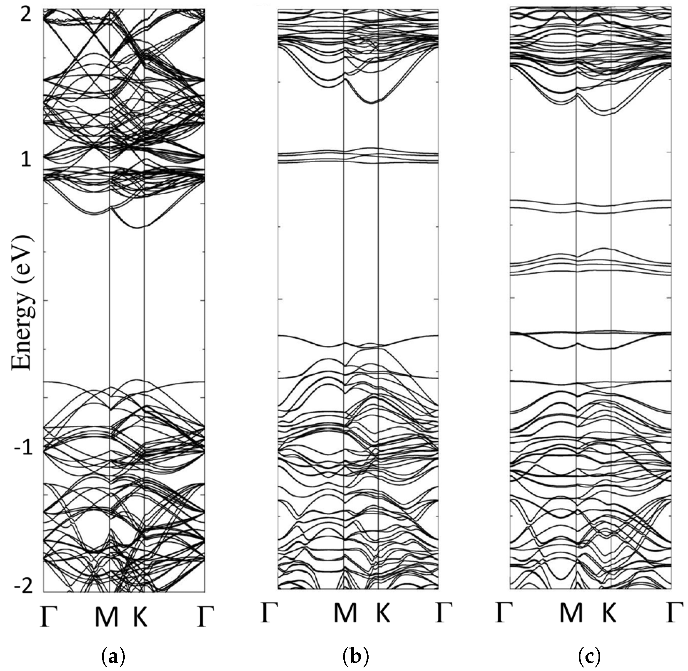
6.1. Band Structures
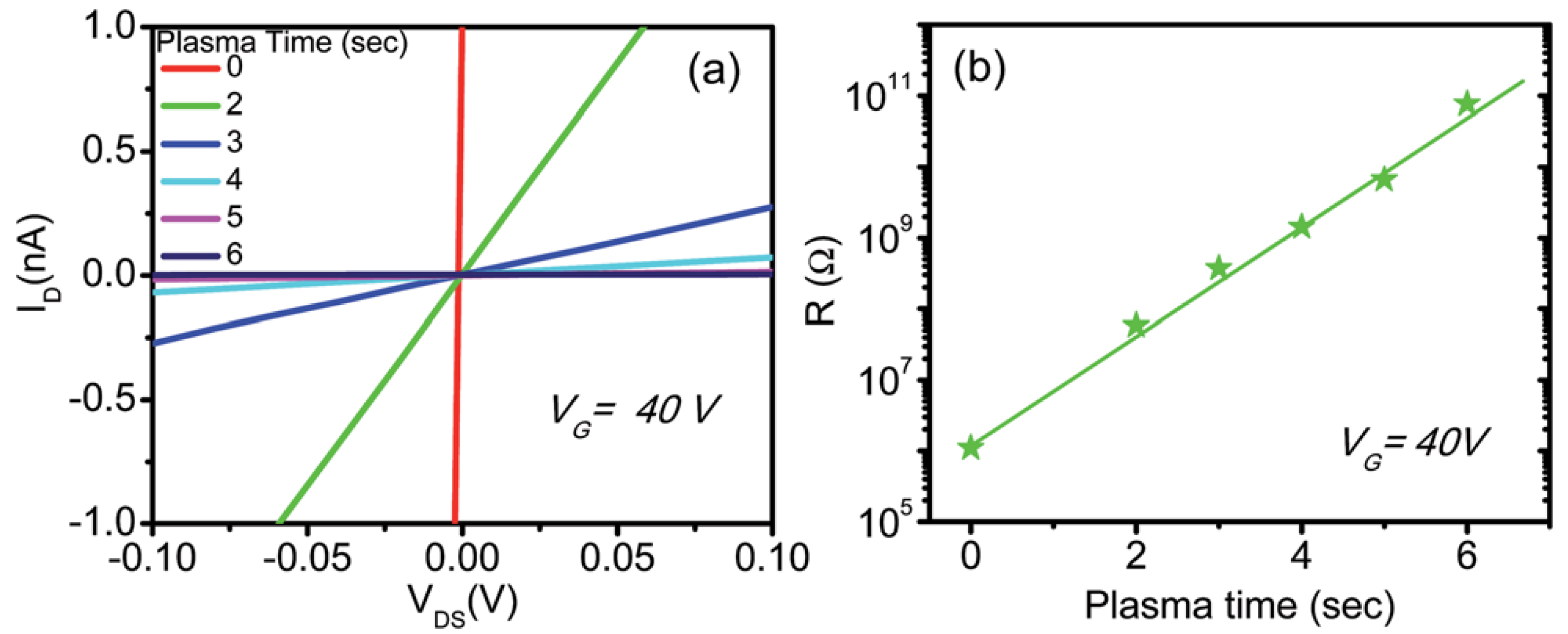
6.2. Electric Properties
6.3. Catalytic Properties
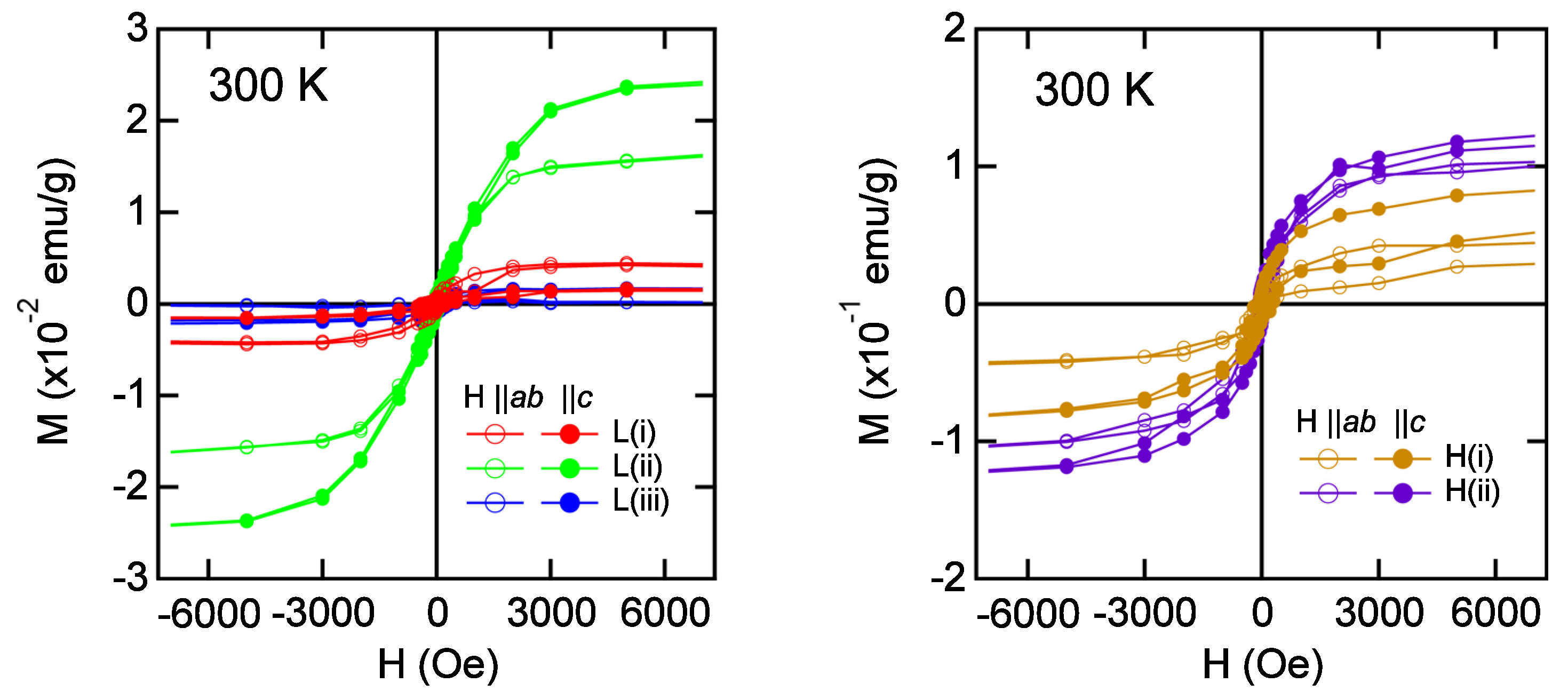
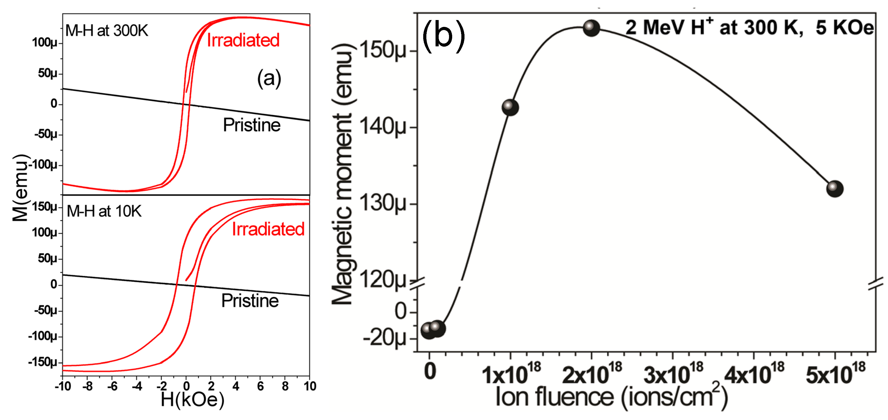
6.4. Magnetic Properties
7. Conclusions and Outlook
Author Contributions
Funding
Acknowledgments
Conflicts of Interest
Abbreviations
| 2D | two-dimensional |
| AFM | atomic force microscopy |
| CBM | conduction band minimum |
| CVD | chemical vapor deposition |
| EBI | electron-beam irradiation |
| EBIT | electron-beam ion trap |
| EBL | electron-beam lithography |
| EDS | electron X-ray dispersive spectroscopy |
| EDX | energy-dispersive X-ray spectroscopy |
| EPMA | electron probe micro-analyzer |
| FET | field effect transistor |
| FFT | fast Fourier transformation |
| FIB | focused ion beam |
| FWHM | full width at half maximum |
| GANIL | The Grand Accélérateur National d’Ions Lourds (Large Heavy Ion National Accelerator) |
| HAADF | high angle annular dark-field |
| HER | hydrogen evolution reaction |
| HIM | helium-ion microscopy |
| HIRFL | heavy ion Research facility in Lanzhou |
| HRTEM | high-resolution transmission electron microscopy |
| IBAD | ion-beam assisted deposition |
| LEAF | low-energy accelerator facility |
| MBE | molecular beam epitaxy |
| NEMS | nanoelectromechanical systems |
| PAMBE | plasma-assisted molecular beam epitaxy |
| PL | photoluminescence |
| RF | radio-frequency |
| RT | room temperature |
| SAED | selected-area electron diffraction |
| SEM | scanning electron microscopy |
| STEM | scanning transmission electron microscopy |
| STM | scanning tunneling microscope |
| TMDC | Transition-metal dichalcogenides |
| TEM | transmission electron microscopy |
| TOF-SIMS | time-of-flight secondary ion mass spectrometry |
| UV | ultraviolet |
| UHV | ultra-high vacuum |
| VBM | valence band maximum |
| VUV | vacuum ultraviolet |
| XPS | X-ray photoelectron spectroscopy |
| XRD | X-ray diffraction |
References
- Kroto, H.W.; Heath, J.R.; O’Brien, S.C.; Curl, R.F.; Smalley, R.E. C60: Buckminsterfullerene. Nature 1985, 318, 162–163. [Google Scholar] [CrossRef]
- Iijima, S.; Ichihashi, T. Single-shell carbon nanotubes of 1-nm diameter. Nature 1993, 363, 603–605. [Google Scholar] [CrossRef]
- Bethune, D.S.; Kiang, C.H.; de Vries, M.S.; Gorman, G.; Savoy, R.; Vazquez, J.; Beyers, R. Cobalt-catalysed growth of carbon nanotubes with single-atomic-layer walls. Nature 1993, 363, 605–607. [Google Scholar] [CrossRef]
- Novoselov, K.S.; Geim, A.K.; Morozov, S.V.; Jiang, D.; Zhang, Y.; Dubonos, S.V.; Grigorieva, I.V.; Firsov, A.A. Electric field effect in atomically thin carbon films. Science 2004, 306, 666–669. [Google Scholar] [CrossRef]
- Frindt, R.F. Single crystals of MoS2 several molecular layers thick. J. Appl. Phys. 1966, 37, 1928–1929. [Google Scholar] [CrossRef]
- Spalvins, T. Lubrication with sputtered MoS2 films: Principles, operation, and limitations. J. Mater. Eng. Perform. 1992, 1, 347–351. [Google Scholar] [CrossRef]
- Chhowalla, M.; Amaratunga, G.A.J. Thin films of fullerene-like MoS2 nanoparticles with ultra-low friction and wear. Nature 2000, 407, 164–167. [Google Scholar] [CrossRef] [PubMed]
- Jaramillo, T.F.; Jørgensen, K.P.; Bonde, J.; Nielsen, J.H.; Horch, S.; Chorkendorff, I. Identification of active edge sites for electrochemical H2 evolution from MoS2 nanocatalysts. Science 2007, 317, 100–102. [Google Scholar] [CrossRef]
- Roxlo, C.B.; Deckman, H.W.; Gland, J.; Cameron, S.D.; Chianelli, R.R. Edge surfaces in lithographically textured molybdenum disulfide. Science 1987, 235, 1629–1631. [Google Scholar] [CrossRef]
- Chianelli, R.R.; Siadati, M.H.; De la Rosa, M.P.; Berhault, G.; Wilcoxon, J.P.; Bearden, R.; Abrams, B.L. Catalytic properties of single layers of transition metal sulfide catalytic materials. Catal. Rev. 2006, 48, 1–41. [Google Scholar] [CrossRef]
- Wang, Q.H.; Kalantar-Zadeh, K.; Kis, A.; Coleman, J.N.; Strano, M.S. Electronics and optoelectronics of two-dimensional transition metal dichalcogenides. Nat. Nanotechnol. 2012, 7, 699–712. [Google Scholar] [CrossRef] [PubMed]
- Peng, Q.; De, S. Outstanding mechanical properties of monolayer MoS2 and its application in elastic energy storage. Phys. Chem. Chem. Phys. 2013, 15, 19427–19437. [Google Scholar] [CrossRef] [PubMed]
- Fiori, G.; Bonaccorso, F.; Iannaccone, G.; Palacios, T.; Neumaier, D.; Seabaugh, A.; Banerjee, S.K.; Colombo, L. Electronics based on two-dimensional materials. Nat. Nanotechnol. 2014, 9, 768–779. [Google Scholar] [CrossRef] [PubMed]
- Lembke, D.; Bertolazzi, S.; Kis, A. Single-layer MoS2 electronics. Acc. Chem. Res. 2015, 48, 100–110. [Google Scholar] [CrossRef] [PubMed]
- Radisavljevic, B.; Radenovic, A.; Brivio, J.; Giacometti, V.; Kis, A. Single-layer MoS2 transistors. Nat. Nanotechnol. 2011, 6, 147–150. [Google Scholar] [CrossRef] [PubMed]
- Sarkar, D.; Liu, W.; Xie, X.; Anselmo, A.C.; Mitragotri, S.; Banerjee, K. MoS2 field-effect transistor for next-generation label-free biosensors. ACS Nano 2014, 8, 3992–4003. [Google Scholar] [CrossRef] [PubMed]
- Kim, J.S.; Yoo, H.W.; Choi, H.O.; Jung, H.T. Tunable volatile organic compounds sensor by using thiolated ligand conjugation on MoS2. Nano Lett. 2014, 14, 5941–5947. [Google Scholar] [CrossRef]
- Yazyev, O.V.; Kis, A. MoS2 and semiconductors in the flatland. Mater. Today 2015, 18, 20–30. [Google Scholar] [CrossRef]
- Nguyen, T.P.; Van Le, Q.; Choi, K.S.; Oh, J.H.; Kim, Y.G.; Lee, S.M.; Chang, S.T.; Cho, Y.H.; Choi, S.; Kim, T.Y.; et al. MoS2 nanosheets exfoliated by sonication and their application in organic photovoltaic cells. Sci. Adv. Mater. 2015, 7, 700–705. [Google Scholar] [CrossRef]
- Li, H.; Tsai, C.; Koh, A.L.; Cai, L.; Contryman, A.W.; Fragapane, A.H.; Zhao, J.; Han, H.S.; Manoharan, H.C.; Abild-Pedersen, F.; et al. Activating and optimizing MoS2 basal planes for hydrogen evolution through the formation of strained sulphur vacancies. Nat. Mater. 2016, 15, 48–53. [Google Scholar] [CrossRef]
- Yu, Z.; Pan, Y.; Shen, Y.; Wang, Z.; Ong, Z.Y.; Xu, T.; Xin, R.; Pan, L.; Wang, B.; Sun, L.; et al. Towards intrinsic charge transport in monolayer molybdenum disulfide by defect and interface engineering. Nat. Commun. 2014, 5, 5290. [Google Scholar] [CrossRef] [PubMed]
- Sim, D.M.; Kim, M.; Yim, S.; Choi, M.J.; Choi, J.; Yoo, S.; Jung, Y.S. Controlled doping of vacancy-containing few-layer MoS2 via highly stable thiol-based molecular chemisorption. ACS Nano 2015, 9, 12115–12123. [Google Scholar] [CrossRef] [PubMed]
- Nguyen, E.P.; Carey, B.J.; Ou, J.Z.; van Embden, J.; Gaspera, E.D.; Chrimes, A.F.; Spencer, M.J.S.; Zhuiykov, S.; Kalantar-zadeh, K.; Daeneke, T. Electronic tuning of 2D MoS2 through surface functionalization. Adv. Mater. 2015, 27, 6225–6229. [Google Scholar] [CrossRef] [PubMed]
- Cho, K.; Min, M.; Kim, T.Y.; Jeong, H.; Pak, J.; Kim, J.K.; Jang, J.; Yun, S.J.; Lee, Y.H.; Hong, W.K.; et al. Electrical and optical characterization of MoS2 with sulfur vacancy passivation by treatment with alkanethiol molecules. ACS Nano 2015, 9, 8044–8053. [Google Scholar] [CrossRef] [PubMed]
- Walker, R.C.; Shi, T.; Silva, E.C.; Jovanovic, I.; Robinson, J.A. Radiation effects on two-dimensional materials. Phys. Status Solidi 2016, 213, 3065–3077. [Google Scholar] [CrossRef]
- Peng, Q.; Crean, J.; Dearden, A.K.; Huang, C.; Wen, X.; Bordas, S.P.A.; De, S. Defect engineering of 2D monatomic-layer materials. Mod. Phys. Lett. B 2013, 27, 1330017. [Google Scholar] [CrossRef]
- Yang, D.; Sandoval, S.J.; Divigalpitiya, W.M.R.; Irwin, J.C.; Frindt, R.F. Structure of single-molecular-layer MoS2. Phys. Rev. B 1991, 43, 12053–12056. [Google Scholar] [CrossRef]
- Wypych, F.; Schöllhorn, R. 1T-MoS2, a new metallic modification of molybdenum disulfide. J. Chem. Soc. Chem. Commun. 1992, 19, 1386–1388. [Google Scholar] [CrossRef]
- Benavente, E.; Santa Ana, M.A.; Mendizábal, F.; González, G. Intercalation chemistry of molybdenum disulfide. Coord. Chem. Rev. 2002, 224, 87–109. [Google Scholar] [CrossRef]
- Fan, X.; Xu, P.; Zhou, D.; Sun, Y.; Li, Y.C.; Nguyen, M.A.T.; Terrones, M.; Mallouk, T.E. Fast and efficient preparation of exfoliated 2H MoS2 nanosheets by sonication-assisted lithium intercalation and infrared laser-induced 1T to 2H phase reversion. Nano Lett. 2015, 15, 5956–5960. [Google Scholar] [CrossRef]
- Xu, D.; Zhu, Y.; Liu, J.; Li, Y.; Peng, W.; Zhang, G.; Zhang, F.; Fan, X. Microwave-assisted 1T to 2H phase reversion of MoS2 in solution: A fast route to processable dispersions of 2H-MoS2 nanosheets and nanocomposites. Nanotechnology 2016, 27, 385604. [Google Scholar] [CrossRef] [PubMed]
- Bromley, R.A.; Murray, R.B.; Yoffe, A.D. The band structures of some transition metal dichalcogenides. III. Group VIA: Trigonal prism materials. J. Phys. C 1972, 5, 759. [Google Scholar] [CrossRef]
- Wieting, T.J.; Verble, J.L. Infrared and Raman studies of long-wavelength optical phonons in hexagonal MoS2. Phys. Rev. B 1971, 3, 4286–4292. [Google Scholar] [CrossRef]
- Mattheiss, L.F. Band structures of transition-metal-dichalcogenide layer compounds. Phys. Rev. B 1973, 8, 3719–3740. [Google Scholar] [CrossRef]
- Böker, T.; Severin, R.; Müller, A.; Janowitz, C.; Manzke, R.; Voβ, D.; Krüger, P.; Mazur, A.; Pollmann, J. Band structure of MoS2, MoSe2, and α-MoTe2: Angle-resolved photoelectron spectroscopy and ab initio calculations. Phys. Rev. B 2001, 64, 235305. [Google Scholar] [CrossRef]
- Kam, K.K.; Parkinson, B.A. Detailed photocurrent spectroscopy of the semiconducting group VIB transition metal dichalcogenides. J. Phys. Chem. 1982, 86, 463–467. [Google Scholar] [CrossRef]
- Yun, W.S.; Han, S.W.; Hong, S.C.; Kim, I.G.; Lee, J.D. Thickness and strain effects on electronic structures of transition metal dichalcogenides: 2H-MX2 semiconductors (M = Mo, W; X = S, Se, Te). Phys. Rev. B 2012, 85, 033305. [Google Scholar] [CrossRef]
- Mak, K.F.; Lee, C.; Hone, J.; Shan, J.; Heinz, T.F. Atomically thin MoS2: A new direct-gap semiconductor. Phys. Rev. Lett. 2010, 105, 136805. [Google Scholar] [CrossRef]
- Splendiani, A.; Sun, L.; Zhang, Y.; Li, T.; Kim, J.; Chim, C.Y.; Galli, G.; Wang, F. Emerging photoluminescence in monolayer MoS2. Nano Lett. 2010, 10, 1271–1275. [Google Scholar] [CrossRef]
- Yang, T.; Feng, J.; Liu, X.; Wang, Y.; Ge, H.; Cao, D.; Li, H.; Peng, Q.; Ramos, M.; Wen, X.D.; et al. A combined computational and experimental study of the adsorption of sulfur containing molecules on molybdenum disulfide nanoparticles. J. Mater. Res. 2018, 33, 3589–3603. [Google Scholar] [CrossRef]
- Chhowalla, M.; Shin, H.S.; Eda, G.; Li, L.J.; Loh, K.P.; Zhang, H. The chemistry of two-dimensional layered transition metal dichalcogenide nanosheets. Nat. Chem. 2013, 5, 263–275. [Google Scholar] [CrossRef] [PubMed]
- Ganatra, R.; Zhang, Q. Few-layer MoS2: A promising layered semiconductor. ACS Nano 2014, 8, 4074–4099. [Google Scholar] [CrossRef] [PubMed]
- Jiang, J.W. Graphene versus MoS2: A short review. Front. Phys. 2015, 10, 287–302. [Google Scholar] [CrossRef]
- Wang, H.; Li, C.; Fang, P.; Zhang, Z.; Zhang, J.Z. Synthesis, properties, and optoelectronic applications of two-dimensional MoS2 and MoS2-based heterostructures. Chem. Soc. Rev. 2018, 47, 6101–6127. [Google Scholar] [CrossRef] [PubMed]
- Wang, Z.; Mi, B. Environmental applications of 2D molybdenum disulfide (MoS2) nanosheets. Environ. Sci. Technol. 2017, 51, 8229–8244. [Google Scholar] [CrossRef] [PubMed]
- Zhang, X.; Lai, Z.; Tan, C.; Zhang, H. Solution-processed two-dimensional MoS2 nanosheets: Preparation, hybridization, and applications. Angew. Chem. Int. Ed. 2016, 55, 8816–8838. [Google Scholar] [CrossRef] [PubMed]
- Yang, L.; Liu, P.; Li, J.; Xiang, B. Two-dimensional material molybdenum disulfides as electrocatalysts for hydrogen evolution. Catalysts 2017, 7, 285. [Google Scholar] [CrossRef]
- Zhao, Y.; Zhang, Y.; Yang, Z.; Yan, Y.; Sun, K. Synthesis of MoS2 and MoO2 for their applications in H2 generation and lithium ion batteries: A review. Sci. Technol. Adv. Mater. 2013, 14, 043501. [Google Scholar] [CrossRef]
- Theerthagiri, J.; Senthil, R.A.; Senthilkumar, B.; Reddy Polu, A.; Madhavan, J.; Ashokkumar, M. Recent advances in MoS2 nanostructured materials for energy and environmental applications—A review. J. Solid State Chem. 2017, 252, 43–71. [Google Scholar] [CrossRef]
- Laursen, A.B.; Kegnæs, S.; Dahla, S.; Chorkendorff, I. Molybdenum sulfides–efficient and viable materials for electro- and photoelectrocatalytic hydrogen evolution. Energy Environ. Sci. 2012, 5, 5577–5591. [Google Scholar] [CrossRef]
- Ding, Q.; Song, B.; Xu, P.; Jin, S. Efficient electrocatalytic and photoelectrochemical hydrogen generation using MoS2 and related compounds. Chem 2016, 1, 699–726. [Google Scholar] [CrossRef]
- Li, Z.; Meng, X.; Zhang, Z. Recent development on MoS2-based photocatalysis: A review. J. Photochem. Photobiol. C 2018, 35, 39–55. [Google Scholar] [CrossRef]
- Han, B.; Hu, Y.H. MoS2 as a co-catalyst for photocatalytic hydrogen production from water. Energy Sci. Eng. 2016, 4, 285–304. [Google Scholar] [CrossRef]
- Zhang, W.J.; Huang, K.J. A review of recent progress in molybdenum disulfide-based supercapacitors and batteries. Inorg. Chem. Front. 2017, 4, 1602–1620. [Google Scholar] [CrossRef]
- Huang, Y.; Guo, J.; Kang, Y.; Ai, Y.; Li, C.M. Two dimensional atomically thin MoS2 nanosheets and their sensing applications. Nanoscale 2015, 7, 19358–19376. [Google Scholar] [CrossRef]
- Lopez-Sanchez, O.; Lembke, D.; Kayci, M.; Radenovic, A.; Kis, A. Ultrasensitive photodetectors based on monolayer MoS2. Nat. Nanotechnol. 2013, 8, 497–501. [Google Scholar] [CrossRef] [PubMed]
- Yin, Z.; Li, H.; Li, H.; Jiang, L.; Shi, Y.; Sun, Y.; Lu, G.; Zhang, Q.; Chen, X.; Zhang, H. Single-layer MoS2 phototransistors. ACS Nano 2012, 6, 74–80. [Google Scholar] [CrossRef]
- Radisavljevic, B.; Whitwick, M.B.; Kis, A. Integrated circuits and logic operations based on single-layer MoS2. ACS Nano 2011, 5, 9934–9938. [Google Scholar] [CrossRef]
- Liu, Y.; Liu, J. Hybrid nanomaterials of WS2 or MoS2 nanosheets with liposomes: Biointerfaces and multiplexed drug delivery. Nanoscale 2017, 9, 13187–13194. [Google Scholar] [CrossRef]
- Zhang, Z.; Xie, Y.; Peng, Q.; Chen, Y. Thermal transport in MoS2/graphene hybrid nanosheets. Nanotechnology 2015, 26, 375402. [Google Scholar] [CrossRef]
- Zhang, Z.; Xie, Y.; Peng, Q.; Chen, Y. A theoretical prediction of super high-performance thermoelectric materials based on MoS2/WS2 hybrid nanoribbons. Sci. Rep. 2016, 6, 21639. [Google Scholar] [CrossRef] [PubMed]
- Wu, W.; Wang, L.; Li, Y.; Zhang, F.; Lin, L.; Niu, S.; Chenet, D.; Zhang, X.; Hao, Y.; Heinz, T.F.; et al. Piezoelectricity of single-atomic-layer MoS2 for energy conversion and piezotronics. Nature 2014, 514, 470. [Google Scholar] [CrossRef] [PubMed]
- Qi, J.; Lan, Y.W.; Stieg, A.Z.; Chen, J.H.; Zhong, Y.L.; Li, L.J.; Chen, C.D.; Zhang, Y.; Wang, K.L. Piezoelectric effect in chemical vapour deposition-grown atomic-monolayer triangular molybdenum disulfide piezotronics. Nat. Commun. 2015, 6, 7430. [Google Scholar] [CrossRef] [PubMed]
- Feng, J.; Graf, M.; Liu, K.; Ovchinnikov, D.; Dumcenco, D.; Heiranian, M.; Nandigana, V.; Aluru, N.R.; Kis, A.; Radenovic, A. Single-layer MoS2 nanopores as nanopower generators. Nature 2016, 536, 197–200. [Google Scholar] [CrossRef] [PubMed]
- Cao, T.; Wang, G.; Han, W.; Ye, H.; Zhu, C.; Shi, J.; Niu, Q.; Tan, P.; Wang, E.; Liu, B.; et al. Valley-selective circular dichroism of monolayer molybdenum disulphide. Nat. Commun. 2012, 3, 887. [Google Scholar] [CrossRef]
- Venkata Subbaiah, Y.P.; Saji, K.J.; Tiwari, A. Atomically thin MoS2: A versatile nongraphene 2D material. Adv. Funct. Mater. 2016, 26, 2046–2069. [Google Scholar] [CrossRef]
- Dong, R.; Kuljanishvili, I. Review Article: Progress in fabrication of transition metal dichalcogenides heterostructure systems. J. Vac. Sci. Technol. B 2017, 35, 030803. [Google Scholar] [CrossRef]
- Sun, J.; Li, X.; Guo, W.; Zhao, M.; Fan, X.; Dong, Y.; Xu, C.; Deng, J.; Fu, Y. Synthesis methods of two-dimensional MoS2: A brief review. Crystals 2017, 7, 198. [Google Scholar] [CrossRef]
- Merki, D.; Hu, X. Recent developments of molybdenum and tungsten sulfides as hydrogen evolution catalysts. Energy Environ. Sci. 2011, 4, 3878–3888. [Google Scholar] [CrossRef]
- Novoselov, K.S.; Jiang, D.; Schedin, F.; Booth, T.J.; Khotkevich, V.V.; Morozov, S.V.; Geim, A.K. Two-dimensional atomic crystals. Proc. Natl. Acad. Sci. USA 2005, 102, 10451–10453. [Google Scholar] [CrossRef]
- Coleman, J.N.; Lotya, M.; O’Neill, A.; Bergin, S.D.; King, P.J.; Khan, U.; Young, K.; Gaucher, A.; De, S.; Smith, R.J.; et al. Two-dimensional nanosheets produced by liquid exfoliation of layered materials. Science 2011, 331, 568–571. [Google Scholar] [CrossRef]
- Zhou, K.G.; Mao, N.N.; Wang, H.X.; Peng, Y.; Zhang, H.L. A mixed-solvent strategy for efficient exfoliation of inorganic graphene analogues. Angew. Chem. 2011, 123, 11031–11034. [Google Scholar] [CrossRef]
- McDonnell, S.; Addou, R.; Buie, C.; Wallace, R.M.; Hinkle, C.L. Defect-dominated doping and contact resistance in MoS2. ACS Nano 2014, 8, 2880–2888. [Google Scholar] [CrossRef] [PubMed]
- Han, S.W.; Park, Y.; Hwang, Y.H.; Lee, W.G.; Hong, S.C. Investigation of electron irradiation-induced magnetism in layered MoS2 single crystals. Appl. Phys. Lett. 2016, 109, 252403. [Google Scholar] [CrossRef]
- Rotunno, E.; Fabbri, F.; Cinquanta, E.; Kaplan, D.; Longo, M.; Lazzarini, L.; Molle, A.; Swaminathan, V.; Salviati, G. Structural, optical and compositional stability of MoS2 multi-layer flakes under high dose electron beam irradiation. 2D Mater. 2016, 3, 025024. [Google Scholar] [CrossRef]
- Lin, Y.C.; Dumcenco, D.O.; Huang, Y.S.; Suenaga, K. Atomic mechanism of the semiconducting-to-metallic phase transition in single-layered MoS2. Nat. Nanotechnol. 2014, 9, 391–396. [Google Scholar] [CrossRef]
- Karmakar, D.; Halder, R.; Padma, N.; Abraham, G.; Vaibhav, K.; Ghosh, M.; Kaur, M.; Bhattacharya, D.; Rao, T.V.C. Optimal electron irradiation as a tool for functionalization of MoS2: Theoretical and experimental investigation. J. Appl. Phys. 2015, 117, 135701. [Google Scholar] [CrossRef]
- Komsa, H.P.; Kotakoski, J.; Kurasch, S.; Lehtinen, O.; Kaiser, U.; Krasheninnikov, A.V. Two-dimensional transition metal dichalcogenides under electron irradiation: Defect production and doping. Phys. Rev. Lett. 2012, 109, 035503. [Google Scholar] [CrossRef]
- Parkin, W.M.; Balan, A.; Liang, L.; Das, P.M.; Lamparski, M.; Naylor, C.H.; Rodríguez-Manzo, J.A.; Johnson, A.T.C.; Meunier, V.; Drndić, M. Raman shifts in electron-irradiated monolayer MoS2. ACS Nano 2016, 10, 4134–4142. [Google Scholar] [CrossRef]
- Matsunaga, M.; Higuchi, A.; He, G.; Yamada, T.; Krüger, P.; Ochiai, Y.; Gong, Y.; Vajtai, R.; Ajayan, P.M.; Bird, J.P.; et al. Nanoscale-barrier formation induced by low-dose electron-beam exposure in ultrathin MoS2 transistors. ACS Nano 2016, 10, 9730–9737. [Google Scholar] [CrossRef]
- Liu, X.; Xu, T.; Wu, X.; Zhang, Z.; Yu, J.; Qiu, H.; Hong, J.H.; Jin, C.H.; Li, J.X.; Wang, X.R.; et al. Top–down fabrication of sub-nanometre semiconducting nanoribbons derived from molybdenum disulfide sheets. Nat. Commun. 2013, 4, 1776. [Google Scholar] [CrossRef] [PubMed]
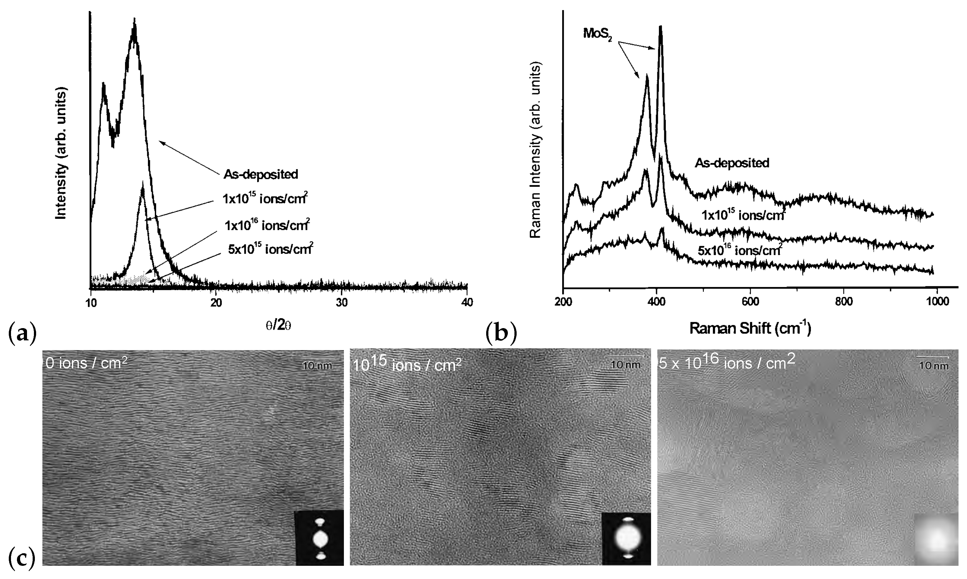
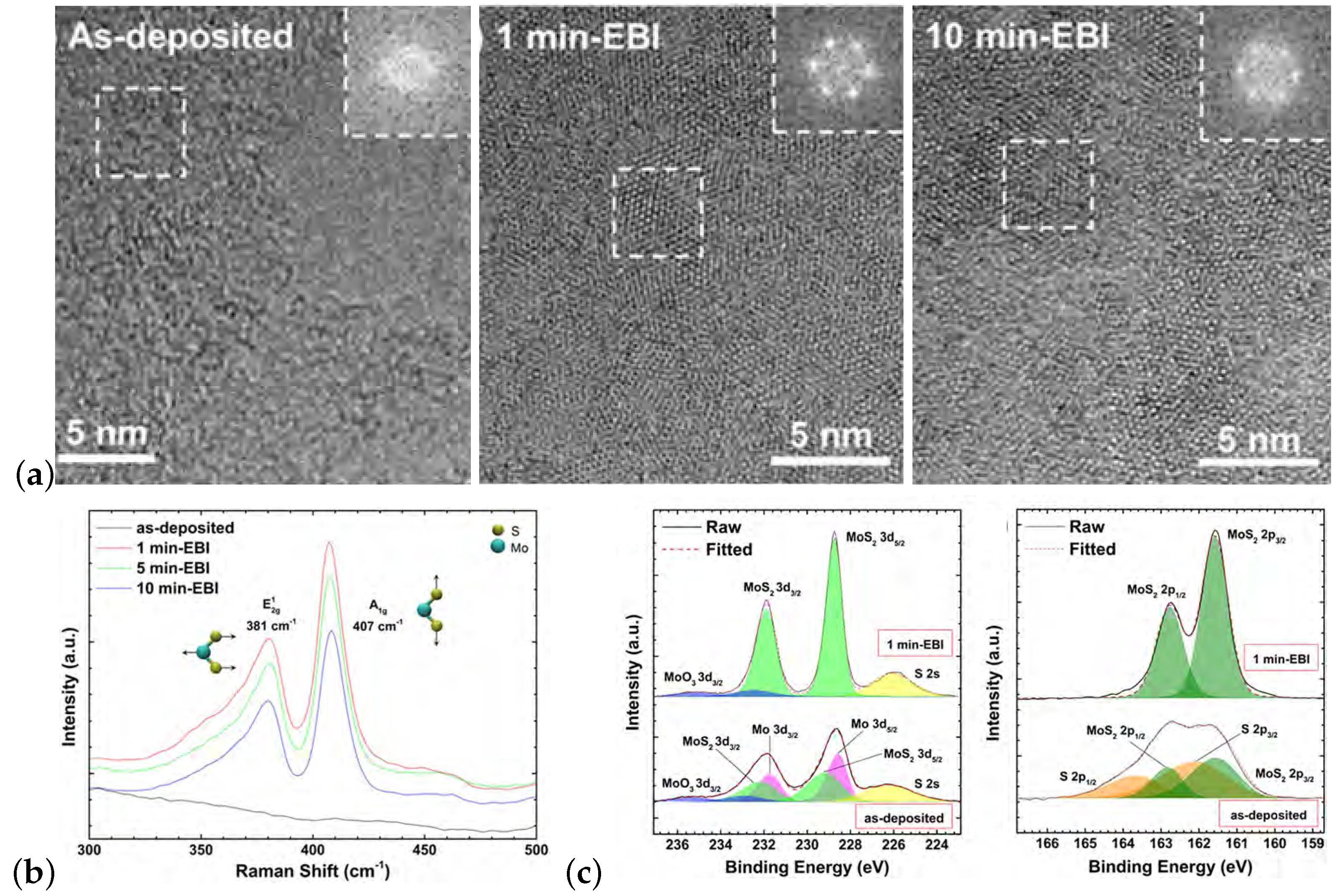
- Kim, B.H.; Gu, H.H.; Yoon, Y.J. Atomic rearrangement of a sputtered MoS2 film from amorphous to a 2D layered structure by electron beam irradiation. Sci. Rep. 2017, 7, 3874. [Google Scholar] [CrossRef] [PubMed]
- Ochedowski, O.; Marinov, K.; Wilbs, G.; Keller, G.; Scheuschner, N.; Severin, D.; Bender, M.; Maultzsch, J.; Tegude, F.J.; Schleberger, M. Radiation hardness of graphene and MoS2 field effect devices against swift heavy ion irradiation. J. Appl. Phys. 2013, 113, 214306. [Google Scholar] [CrossRef]
- Bae, S.; Sugiyama, N.; Matsuo, T.; Raebiger, H.; Shudo, K.I.; Ohno, K. Defect-induced vibration modes of Ar+-irradiated MoS2. Phys. Rev. Appl. 2017, 7, 024001. [Google Scholar] [CrossRef]
- Mathew, S.; Gopinadhan, K.; Chan, T.K.; Yu, X.J.; Zhan, D.; Cao, L.; Rusydi, A.; Breese, M.B.H.; Dhar, S.; Shen, Z.X.; et al. Magnetism in MoS2 induced by proton irradiation. Appl. Phys. Lett. 2012, 101, 102103. [Google Scholar] [CrossRef]
- Kim, T.Y.; Cho, K.; Park, W.; Park, J.; Song, Y.; Hong, S.; Hong, W.K.; Lee, T. Irradiation effects of high-energy proton beams on MoS2 field effect transistors. ACS Nano 2014, 8, 2774–2781. [Google Scholar] [CrossRef] [PubMed]
- Wang, B.; Yang, S.; Chen, J.; Mann, C.; Bushmaker, A.; Cronin, S.B. Radiation-induced direct bandgap transition in few-layer MoS2. Appl. Phys. Lett. 2017, 111, 131101. [Google Scholar] [CrossRef]
- Isherwood, L.H.; Worsley, R.E.; Casiraghi, C.; Baidak, A. Alpha particle irradiation of bulk and exfoliated MoS2 and WS2 membranes. Nucl. Instrum. Methods Phys. Res. Sect. B 2018, 435, 180–189. [Google Scholar] [CrossRef]
- Fox, D.S.; Zhou, Y.; Maguire, P.; O’Neill, A.; Ó’Coileáin, C.; Gatensby, R.; Glushenkov, A.M.; Tao, T.; Duesberg, G.S.; Shvets, I.V.; et al. Nanopatterning and electrical tuning of MoS2 layers with a subnanometer helium ion beam. Nano Lett. 2015, 15, 5307–5313. [Google Scholar] [CrossRef]
- Tongay, S.; Suh, J.; Ataca, C.; Fan, W.; Luce, A.; Kang, J.S.; Liu, J.; Ko, C.; Raghunathanan, R.; Zhou, J.; et al. Defects activated photoluminescence in two-dimensional semiconductors: Interplay between bound, charged, and free excitons. Sci. Rep. 2013, 3, 2657. [Google Scholar] [CrossRef]
- Klein, J.; Kuc, A.; Nolinder, A.; Altzschner, M.; Wierzbowski, J.; Sigger, F.; Kreupl, F.; Finley, J.J.; Wurstbauer, U.; Holleitner, A.W.; et al. Robust valley polarization of helium ion modified atomically thin MoS2. 2D Mater. 2018, 5, 011007. [Google Scholar] [CrossRef]
- Maguire, P.; Fox, D.S.; Zhou, Y.; Wang, Q.; O’Brien, M.; Jadwiszczak, J.; Cullen, C.P.; McManus, J.; Bateman, S.; McEvoy, N.; et al. Defect sizing, separation, and substrate effects in ion-irradiated monolayer two-dimensional materials. Phys. Rev. B 2018, 98, 134109. [Google Scholar] [CrossRef]
- Inoue, A.; Komori, T.; Shudo, K.I. Atomic-scale structures and electronic states of defects on Ar+-ion irradiated MoS2. J. Electron Spectrosc. Relat. Phenom. 2013, 189, 11–18. [Google Scholar] [CrossRef]
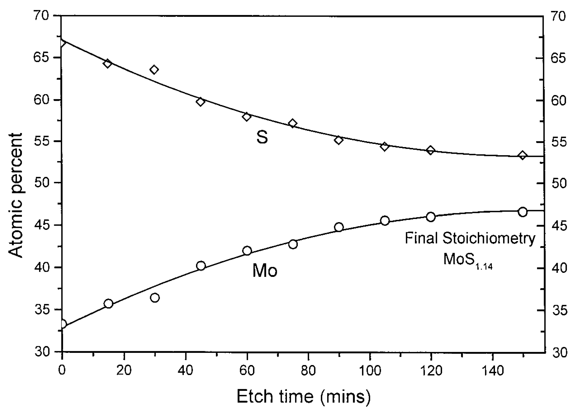
- Baker, M.A.; Gilmore, R.; Lenardi, C.; Gissler, W. XPS investigation of preferential sputtering of S from MoS2 and determination of MoSx stoichiometry from Mo and S peak positions. Appl. Surf. Sci. 1999, 150, 255–262. [Google Scholar] [CrossRef]
- Wahl, K.J.; Dunn, D.N.; Singer, I.L. Effects of ion implantation on microstructure, endurance and wear behavior of IBAD MoS2. Wear 2000, 237, 1–11. [Google Scholar] [CrossRef]
- Ma, Q.; Odenthal, P.M.; Mann, J.; Le, D.; Wang, C.S.; Zhu, Y.; Chen, T.; Sun, D.; Yamaguchi, K.; Tran, T.; et al. Controlled argon beam-induced desulfurization of monolayer molybdenum disulfide. J. Phys. Condens. Matter 2013, 25, 252201. [Google Scholar] [CrossRef] [PubMed]
- Zhu, J.; Wang, Z.; Yu, H.; Li, N.; Zhang, J.; Meng, J.; Liao, M.; Zhao, J.; Lu, X.; Du, L.; et al. Argon plasma induced phase transition in monolayer MoS2. J. Am. Chem. Soc. 2017, 139, 10216–10219. [Google Scholar] [CrossRef] [PubMed]
- Mishra, P.; Tangi, M.; Ng, T.K.; Hedhili, M.N.; Anjum, D.H.; Alias, M.S.; Tseng, C.C.; Li, L.J.; Ooi, B.S. Impact of N-plasma and Ga-irradiation on MoS2 layer in molecular beam epitaxy. Appl. Phys. Lett. 2017, 110, 012101. [Google Scholar] [CrossRef]
- Thiruraman, J.P.; Fujisawa, K.; Danda, G.; Das, P.M.; Zhang, T.; Bolotsky, A.; Perea-López, N.; Nicolaï, A.; Senet, P.; Terrones, M.; et al. Angstrom-size defect creation and ionic transport through pores in single-layer MoS2. Nano Lett. 2018, 18, 1651–1659. [Google Scholar] [CrossRef]
- Madauβ, L.; Ochedowski, O.; Lebius, H.; Ban-d’Etat, B.; Naylor, C.H.; Johnson, A.T.C.; Kotakoski, J.; Schleberger, M. Defect engineering of single- and few-layer MoS2 by swift heavy ion irradiation. 2D Mater. 2017, 4, 015034. [Google Scholar] [CrossRef]
- Hopster, J.; Kozubek, R.; Krämer, J.; Sokolovsky, V.; Schleberger, M. Ultra-thin MoS2 irradiated with highly charged ions. Nucl. Instrum. Methods Phys. Res. Sect. B 2013, 317, 165–169. [Google Scholar] [CrossRef]
- Guo, H.; Sun, Y.; Zhai, P.; Yao, H.; Zeng, J.; Zhang, S.; Duan, J.; Hou, M.; Khan, M.; Liu, J. Swift-heavy ion irradiation-induced latent tracks in few- and mono-layer MoS2. Appl. Phys. A 2016, 122, 375. [Google Scholar] [CrossRef]
- Mignuzzi, S.; Pollard, A.J.; Bonini, N.; Brennan, B.; Gilmore, I.S.; Pimenta, M.A.; Richards, D.; Roy, D. Effect of disorder on Raman scattering of single-layer MoS2. Phys. Rev. B 2015, 91, 195411. [Google Scholar] [CrossRef]
- Henry, J.; Dunlop, A.; Della-Negra, S. Craters, bumps and onion structures in MoS2 irradiated with MeV C60 ions. Nucl. Instrum. Methods Phys. Res. Sect. B 1998, 146, 405–411. [Google Scholar] [CrossRef]
- Devine, M.J.; Lamson, E.R.; Bowen, J.H. Inorganic solid film lubricants. J. Chem. Eng. Data 1961, 6, 79–82. [Google Scholar] [CrossRef]
- Lee, J.; Krupcale, M.J.; Feng, P.X.L. Effects of γ-ray radiation on two-dimensional molybdenum disulfide (MoS2) nanomechanical resonators. Appl. Phys. Lett. 2016, 108, 023106. [Google Scholar] [CrossRef]
- Ozden, B.; Khanal, M.P.; Park, J.; Uprety, S.; Mirkhani, V.; Yapabandara, K.; Kim, K.; Kuroda, M.; Bozack, M.J.; Choi, W.; et al. Raman and X-ray photoelectron spectroscopy investigation of the effect of gamma-ray irradiation on MoS2. Micro Nano Lett. 2017, 12, 271–274. [Google Scholar] [CrossRef]
- Coleman, A.F.; Flores, R.L.; Xu, Y.Q. Effects of ozone plasma treatment and X-ray irradiation on optical properties of atomically thin molybdenum disulfide. Young Sci. 2014, 4, 4. [Google Scholar] [CrossRef]
- Azcatl, A.; McDonnell, S.; Santosh, K.C.; Peng, X.; Dong, H.; Qin, X.; Addou, R.; Mordi, G.I.; Lu, N.; Kim, J.; et al. MoS2 functionalization for ultra-thin atomic layer deposited dielectrics. Appl. Phys. Lett. 2014, 104, 111601. [Google Scholar] [CrossRef]
- McMorrow, J.J.; Cress, C.D.; Arnold, H.N.; Sangwan, V.K.; Jariwala, D.; Schmucker, S.W.; Marks, T.J.; Hersam, M.C. Vacuum ultraviolet radiation effects on two-dimensional MoS2 field-effect transistors. Appl. Phys. Lett. 2017, 110, 073102. [Google Scholar] [CrossRef]
- Gu, E.; Wang, Q.; Zhang, Y.; Cong, C.; Hu, L.; Tian, P.; Liu, R.; Zhang, S.L.; Qiu, Z.J. A real-time Raman spectroscopy study of the dynamics of laser-thinning of MoS2 flakes to monolayers. AIP Adv. 2017, 7, 125329. [Google Scholar] [CrossRef]
- Lu, J.; Lu, J.H.; Liu, H.; Liu, B.; Chan, K.X.; Lin, J.; Chen, W.; Loh, K.P.; Sow, C.H. Improved photoelectrical properties of MoS2 films after laser micromachining. ACS Nano 2014, 8, 6334–6343. [Google Scholar] [CrossRef] [PubMed]
- Paradisanos, I.; Kymakis, E.; Fotakis, C.; Kioseoglou, G.; Stratakis, E. Intense femtosecond photoexcitation of bulk and monolayer MoS2. Appl. Phys. Lett. 2014, 105, 041108. [Google Scholar] [CrossRef]
- Zhai, P.; Lu, F.; Tang, X.; Wei, J.; He, J.; Shang, G.; Yao, J. Observation of radiation damage of energetic heavy ions impacts on MoS2 surface by scanning tunneling microscopy. Sci. China Ser. A 1993, 36, 715–719. [Google Scholar] [CrossRef]
- Bhattacharya, R.S.; Rai, A.K.; McCormick, A.W.; Erdemir, A. High energy (MeV) ion beam modifications of sputtered MoS2 coatings on ceramics. Tribol. Trans. 1993, 36, 621–626. [Google Scholar] [CrossRef]
- Murray, R.; Haynes, K.; Zhao, X.; Perry, S.; Hatem, C.; Jones, K. The effect of low energy ion implantation on MoS2. ECS J. Solid State Sci. Technol. 2016, 5, Q3050–Q3053. [Google Scholar] [CrossRef]
- Chen, Y.; Huang, S.; Ji, X.; Adepalli, K.; Yin, K.; Ling, X.; Wang, X.; Xue, J.; Dresselhaus, M.; Kong, J.; et al. Tuning electronic structure of single layer MoS2 through defect and interface engineering. ACS Nano 2018, 12, 2569–2579. [Google Scholar] [CrossRef] [PubMed]
- Liu, Y.; Nan, H.; Wu, X.; Pan, W.; Wang, W.; Bai, J.; Zhao, W.; Sun, L.; Wang, X.; Ni, Z. Layer-by-layer thinning of MoS2 by plasma. ACS Nano 2013, 7, 4202–4209. [Google Scholar] [CrossRef]
- Elgqvist, J.; Frost, S.; Pouget, J.P.; Albertsson, P. The potential and hurdles of targeted alpha therapy—Clinical trials and beyond. Front. Oncol. 2014, 3, 324. [Google Scholar] [CrossRef]
- Sgouros, G.; Hobbs, R.F.; Song, H. Modelling and dosimetry for alpha-particle therapy. Curr. Radiopharm. 2011, 4, 261–265. [Google Scholar] [CrossRef]
- Zhang, H.; Maguire, P.; Fox, D.S.; Zhou, Y. Beam exfoliation of MoS2 layers with a helium ion beam. In Proceedings of the European Microscopy Congress 2016, Lyon, France, 28 August–2 September 2016; p. 1. [Google Scholar] [CrossRef]
- Han, S.W.; Park, Y.; Hwang, Y.H.; Jekal, S.; Kang, M.; Lee, W.G.; Yang, W.; Lee, G.D.; Hong, S.C. Electron beam-formed ferromagnetic defects on MoS2 surface along 1 T phase transition. Sci. Rep. 2016, 6, 38730. [Google Scholar] [CrossRef] [PubMed]
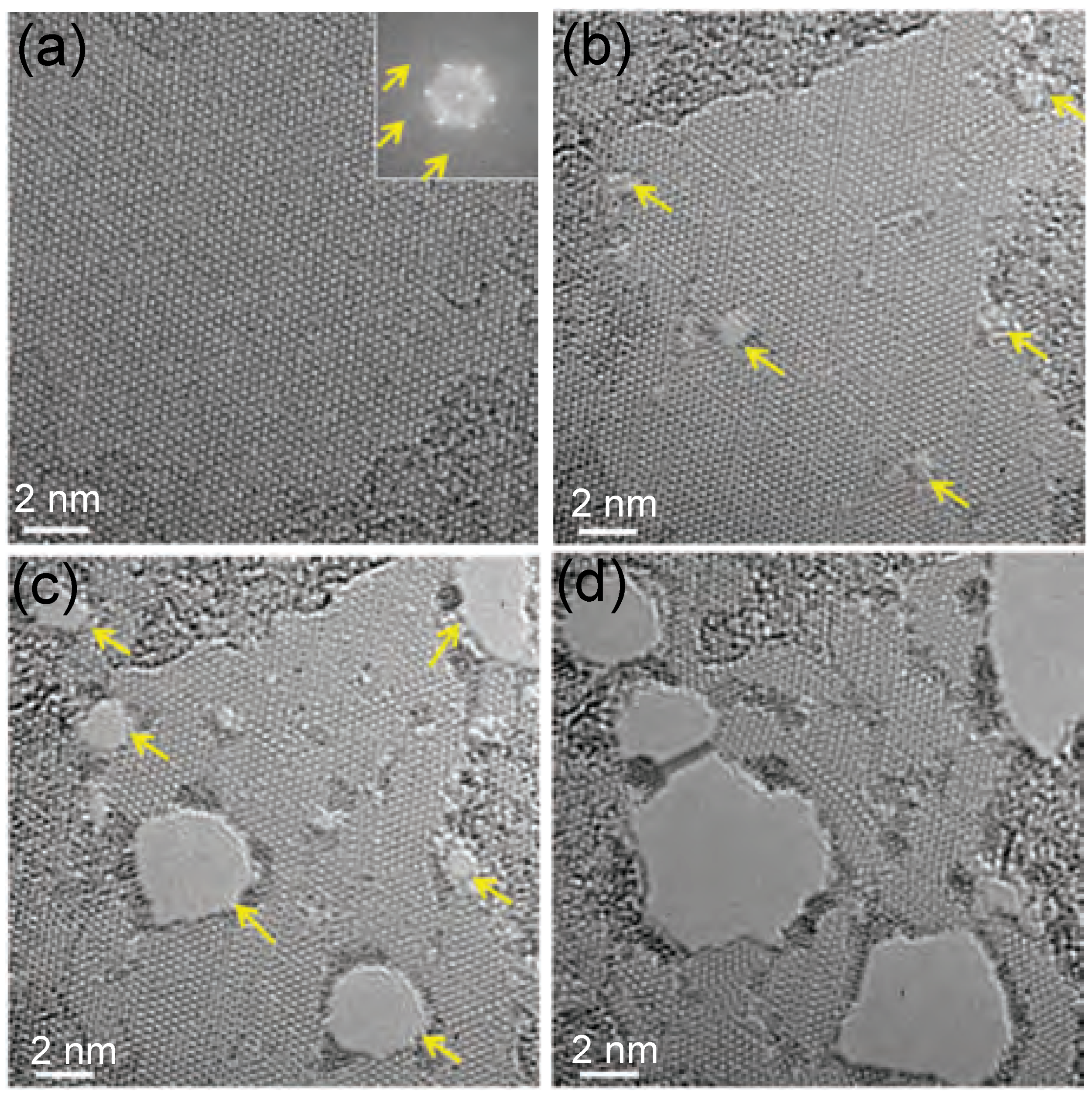
- Komsa, H.P.; Kurasch, S.; Lehtinen, O.; Kaiser, U.; Krasheninnikov, A.V. From point to extended defects in two-dimensional MoS2: Evolution of atomic structure under electron irradiation. Phys. Rev. B 2013, 88, 035301. [Google Scholar] [CrossRef]
- Azcatl, A.; Qin, X.; Prakash, A.; Zhang, C.; Cheng, L.; Wang, Q.; Lu, N.; Kim, M.J.; Kim, J.; Cho, K.; et al. Covalent nitrogen doping and compressive strain in MoS2 by remote N2 plasma exposure. Nano Lett. 2016, 16, 5437–5443. [Google Scholar] [CrossRef] [PubMed]
- Nan, H.; Wang, Z.; Wang, W.; Liang, Z.; Lu, Y.; Chen, Q.; He, D.; Tan, P.; Miao, F.; Wang, X.; et al. Strong photoluminescence enhancement of MoS2 through defect engineering and oxygen bonding. ACS Nano 2014, 8, 5738–5745. [Google Scholar] [CrossRef] [PubMed]
- Chen, M.; Nam, H.; Wi, S.; Ji, L.; Ren, X.; Bian, L.; Lu, S.; Liang, X. Stable few-layer MoS2 rectifying diodes formed by plasma-assisted doping. Appl. Phys. Lett. 2013, 103, 142110. [Google Scholar] [CrossRef]
- Kang, N.; Paudel, H.P.; Leuenberger, M.N.; Tetard, L.; Khondaker, S.I. Photoluminescence quenching in single-layer MoS2 via oxygen plasma treatment. J. Phys. Chem. C 2014, 118, 21258–21263. [Google Scholar] [CrossRef]
- Islam, M.R.; Kang, N.; Bhanu, U.; Paudel, H.P.; Erementchouk, M.; Tetard, L.; Leuenberger, M.N.; Khondaker, S.I. Tuning the electrical property via defect engineering of single layer MoS2 by oxygen plasma. Nanoscale 2014, 6, 10033–10039. [Google Scholar] [CrossRef]
- Ye, G.; Gong, Y.; Lin, J.; Li, B.; He, Y.; Pantelides, S.T.; Zhou, W.; Vajtai, R.; Ajayan, P.M. Defects engineered monolayer MoS2 for improved hydrogen evolution reaction. Nano Lett. 2016, 16, 1097–1103. [Google Scholar] [CrossRef]
- Dhall, R.; Neupane, M.R.; Wickramaratne, D.; Mecklenburg, M.; Li, Z.; Moore, C.; Lake, R.K.; Cronin, S. Direct bandgap transition in many-layer MoS2 by plasma-induced layer decoupling. Adv. Mater. 2015, 27, 1573–1578. [Google Scholar] [CrossRef]
- Kim, M.S.; Nam, G.; Park, S.; Kim, H.; Han, G.H.; Lee, J.; Dhakal, K.P.; Leem, J.Y.; Lee, Y.H.; Kim, J. Photoluminescence wavelength variation of monolayer MoS2 by oxygen plasma treatment. Thin Solid Films 2015, 590, 318–323. [Google Scholar] [CrossRef]
- Nipane, A.; Karmakar, D.; Kaushik, N.; Karande, S.; Lodha, S. Few-layer MoS2 p-type devices enabled by selective doping using low energy phosphorus implantation. ACS Nano 2016, 10, 2128–2137. [Google Scholar] [CrossRef] [PubMed]
- Jadwiszczak, J.; O’Callaghan, C.; Zhou, Y.; Fox, D.S.; Weitz, E.; Keane, D.; Cullen, C.P.; O’Reilly, I.; Downing, C.; Shmeliov, A.; et al. Oxide-mediated recovery of field-effect mobility in plasma-treated MoS2. Sci. Adv. 2018, 4, eaao5031. [Google Scholar] [CrossRef]
- Bhimanapati, G.R.; Hankins, T.; Lei, Y.; Vilá, R.A.; Fuller, I.; Terrones, M.; Robinson, J.A. Growth and tunable surface wettability of vertical MoS2 layers for improved hydrogen evolution reactions. ACS Appl. Mater. Interfaces 2016, 8, 22190–22195. [Google Scholar] [CrossRef]
- Zhang, C.X.; Newaz, A.K.M.; Wang, B.; Zhang, E.X.; Duan, G.X.; Fleetwood, D.M.; Alles, M.L.; Schrimpf, R.D.; Bolotin, K.I.; Pantelides, S.T. Electrical stress and total ionizing dose effects on MoS2 transistors. IEEE Trans. Nucl. Sci. 2014, 61, 2862–2867. [Google Scholar] [CrossRef]
- Li, J.; Wierzbowski, J.; Ceylan, O.; Klein, J.; Nisic, F.; Anh, T.L.; Meggendorfer, F.; Palma, C.A.; Dragonetti, C.; Barth, J.V.; et al. Tuning the optical emission of MoS2 nanosheets using proximal photoswitchable azobenzene molecules. Appl. Phys. Lett. 2014, 105, 241116. [Google Scholar] [CrossRef]
- Lu, X.; Wang, R.; Hao, L.; Yang, F.; Jiao, W.; Peng, P.; Yuan, F.; Liu, W. Oxidative etching of MoS2/WS2 nanosheets to their QDs by facile UV irradiation. Phys. Chem. Chem. Phys. 2016, 18, 31211–31216. [Google Scholar] [CrossRef] [PubMed]
- Singh, A.K.; Andleeb, S.; Singh, J.; Eom, J. Tailoring the electrical properties of multilayer MoS2 transistors using ultraviolet light irradiation. RSC Adv. 2015, 5, 77014–77018. [Google Scholar] [CrossRef]
- Singh, A.K.; Andleeb, S.; Singh, J.; Dung, H.T.; Seo, Y.; Eom, J. Ultraviolet-light-induced reversible and stable carrier modulation in MoS2 field-effect transistors. Adv. Funct. Mater. 2014, 24, 7125–7132. [Google Scholar] [CrossRef]
- Liu, P.; Liu, Y.; Ye, W.; Ma, J.; Gao, D. Flower-like N-doped MoS2 for photocatalytic degradation of RhB by visible light irradiation. Nanotechnology 2016, 27, 225403. [Google Scholar] [CrossRef]
- Castellanos-Gomez, A.; Barkelid, M.; Goossens, A.M.; Calado, V.E.; van der Zant, H.S.J.; Steele, G.A. Laser-thinning of MoS2: On demand generation of a single-layer semiconductor. Nano Lett. 2012, 12, 3187–3192. [Google Scholar] [CrossRef]
- Yoo, J.H.; Kim, E.; Hwang, D.J. Femtosecond laser patterning, synthesis, defect formation, and structural modification of atomic layered materials. MRS Bull. 2016, 41, 1002–1008. [Google Scholar] [CrossRef]
- Pan, Y.; Yang, M.; Li, Y.; Wang, Z.; Zhang, C.; Zhao, Y.; Yao, J.; Wu, Q.; Xu, J. Threshold dependence of deep- and near-subwavelength ripples formation on natural MoS2 induced by femtosecond laser. Sci. Rep. 2016, 6, 19571. [Google Scholar] [CrossRef] [PubMed]
- Windom, B.C.; Sawyer, W.G.; Hahn, D.W. A Raman spectroscopic study of MoS2 and MoO3: Applications to tribological systems. Tribol. Lett. 2011, 42, 301–310. [Google Scholar] [CrossRef]
- Tran Khac, B.C.; Jeon, K.J.; Choi, S.T.; Kim, Y.S.; DelRio, F.W.; Chung, K.H. Laser-induced particle adsorption on atomically thin MoS2. ACS Appl. Mater. Interfaces 2016, 8, 2974–2984. [Google Scholar] [CrossRef] [PubMed]
- Alrasheed, A.; Gorham, J.M.; Tran Khac, B.C.; Alsaffar, F.; DelRio, F.W.; Chung, K.H.; Amer, M.R. Surface properties of laser-treated molybdenum disulfide nanosheets for optoelectronic applications. ACS Appl. Mater. Interfaces 2018, 10, 18104–18112. [Google Scholar] [CrossRef] [PubMed]
- Goswami, A.; Dhandaria, P.; Pal, S.; McGee, R.; Khan, F.; Antić, Ž.; Gaikwad, R.; Prashanthi, K.; Thundat, T. Effect of interface on mid-infrared photothermal response of MoS2 thin film grown by pulsed laser deposition. Nano Res. 2017, 10, 3571–3584. [Google Scholar] [CrossRef]
- Cao, Y.; Gan, S.; Geng, Z.; Liu, J.; Yang, Y.; Bao, Q.; Chen, H. Optically tuned terahertz modulator based on annealed multilayer MoS2. Sci. Rep. 2016, 6, 22899. [Google Scholar] [CrossRef]
- Docherty, C.J.; Parkinson, P.; Joyce, H.J.; Chiu, M.H.; Chen, C.H.; Lee, M.Y.; Li, L.J.; Herz, L.M.; Johnston, M.B. Ultrafast transient terahertz conductivity of monolayer MoS2 and WSe2 grown by chemical vapor deposition. ACS Nano 2014, 8, 11147–11153. [Google Scholar] [CrossRef]
- Arcos, D.; Gabriel, D.; Dumcenco, D.; Kis, A.; Ferrer-Anglada, N. THz time-domain spectroscopy and IR spectroscopy on MoS2. Phys. Status Solidi (b) 2016, 253, 2499–2504. [Google Scholar] [CrossRef]
- Deng, X.Y.; Deng, X.H.; Su, F.H.; Liu, N.H.; Liu, J.T. Broadband ultra-high transmission of terahertz radiation through monolayer MoS2. J. Appl. Phys. 2015, 118, 224304. [Google Scholar] [CrossRef]
- Lee, J.; Wang, Z.; He, K.; Yang, R.; Shan, J.; Feng, P.X.L. Electrically tunable single- and few-layer MoS2 nanoelectromechanical systems with broad dynamic range. Sci. Adv. 2018, 4, eaao6653. [Google Scholar] [CrossRef] [PubMed]
- Krasnozhon, D.; Lembke, D.; Nyffeler, C.; Leblebici, Y.; Kis, A. MoS2 transistors operating at gigahertz frequencies. Nano Lett. 2014, 14, 5905–5911. [Google Scholar] [CrossRef]
- Cheng, R.; Jiang, S.; Chen, Y.; Liu, Y.; Weiss, N.; Cheng, H.C.; Wu, H.; Huang, Y.; Duan, X. Few-layer molybdenum disulfide transistors and circuits for high-speed flexible electronics. Nat. Commun. 2014, 5, 5143. [Google Scholar] [CrossRef] [PubMed]
- Zhang, X.; Hayward, D.O.; Lee, C.; Mingos, D.M.P. Microwave assisted catalytic reduction of sulfur dioxide with methane over MoS2 catalysts. Appl. Catal. B 2001, 33, 137–148. [Google Scholar] [CrossRef]
- Zhao, H.; Mu, X.; Yang, G.; Zheng, C.; Sun, C.; Gao, X.; Wu, T. Microwave-induced activation of additional active edge sites on the MoS2 surface for enhanced Hg0 capture. Appl. Surf. Sci. 2017, 420, 439–445. [Google Scholar] [CrossRef]
- Gao, D.; Si, M.; Li, J.; Zhang, J.; Zhang, Z.; Yang, Z.; Xue, D. Ferromagnetism in freestanding MoS2 nanosheets. Nanoscale Res. Lett. 2013, 8, 129. [Google Scholar] [CrossRef] [PubMed]
- Mdleleni, M.M.; Hyeon, T.; Suslick, K.S. Sonochemical synthesis of nanostructured molybdenum sulfide. J. Am. Chem. Soc. 1998, 120, 6189–6190. [Google Scholar] [CrossRef]
- Petö, J.; Ollár, T.; Vancsó, P.; Popov, Z.I.; Magda, G.Z.; Dobrik, G.; Hwang, C.; Sorokin, P.B.; Tapasztó, L. Spontaneous doping of the basal plane of MoS2 single layers through oxygen substitution under ambient conditions. Nat. Chem. 2018, 10, 1246–1251. [Google Scholar] [CrossRef]
- Donarelli, M.; Bisti, F.; Perrozzi, F.; Ottaviano, L. Tunable sulfur desorption in exfoliated MoS2 by means of thermal annealing in ultra-high vacuum. Chem. Phys. Lett. 2013, 588, 198–202. [Google Scholar] [CrossRef]
- Yamamoto, M.; Einstein, T.L.; Fuhrer, M.S.; Cullen, W.G. Anisotropic etching of atomically thin MoS2. J. Phys. Chem. C 2013, 117, 25643–25649. [Google Scholar] [CrossRef]
- Tongay, S.; Zhou, J.; Ataca, C.; Liu, J.; Kang, J.S.; Matthews, T.S.; You, L.; Li, J.; Grossman, J.C.; Wu, J. Broad-range modulation of light emission in two-dimensional semiconductors by molecular physisorption gating. Nano Lett. 2013, 13, 2831–2836. [Google Scholar] [CrossRef] [PubMed]
- Yang, H.I.; Park, S.; Choi, W. Modification of the optoelectronic properties of two-dimensional MoS2 crystals by ultraviolet-ozone treatment. Appl. Surf. Sci. 2018, 443, 91–96. [Google Scholar] [CrossRef]
- Wang, J.; Li, S.; Zou, X.; Ho, J.; Liao, L.; Xiao, X.; Jiang, C.; Hu, W.; Wang, J.; Li, J. Integration of high-k oxide on MoS2 by using ozone pretreatment for high-performance MoS2 top-gated transistor with thickness-dependent carrier scattering investigation. Small 2015, 11, 5932–5938. [Google Scholar] [CrossRef] [PubMed]
- Le, Q.V.; Nguyen, T.P.; Jang, H.W.; Kim, S.Y. The use of UV/ozone-treated MoS2 nanosheets for extended air stability in organic photovoltaic cells. Phys. Chem. Chem. Phys. 2014, 16, 13123–13128. [Google Scholar] [CrossRef] [PubMed]
- Su, W.; Kumar, N.; Spencer, S.J.; Dai, N.; Roy, D. Transforming bilayer MoS2 into single-layer with strong photoluminescence using UV-ozone oxidation. Nano Res. 2015, 8, 3878–3886. [Google Scholar] [CrossRef]
- Burman, D.; Ghosh, R.; Santra, S.; Ray, S.K.; Guha, P.K. Role of vacancy sites and UV-ozone treatment on few layered MoS2 nanoflakes for toxic gas detection. Nanotechnology 2017, 28, 435502. [Google Scholar] [CrossRef]
- Kretschmer, S.; Maslov, M.; Ghaderzadeh, S.; Ghorbani-Asl, M.; Hlawacek, G.; Krasheninnikov, A.V. Supported two-dimensional materials under ion irradiation: The substrate governs defect production. ACS Appl. Mater. Interfaces 2018, 10, 30827–30836. [Google Scholar] [CrossRef]
- Ghorbani-Asl, M.; Kretschmer, S.; Spearot, D.E.; Krasheninnikov, A.V. Two-dimensional MoS2 under ion irradiation: From controlled defect production to electronic structure engineering. 2D Mater. 2017, 4, 025078. [Google Scholar] [CrossRef]
- Kobayashi, K.; Yamauchi, J. Electronic structure and scanning-tunneling-microscopy image of molybdenum dichalcogenide surfaces. Phys. Rev. B 1995, 51, 17085–17095. [Google Scholar] [CrossRef]
- Gusakova, J.; Wang, X.; Shiau, L.L.; Krivosheeva, A.; Shaposhnikov, V.; Borisenko, V.; Gusakov, V.; Tay, B.K. Electronic properties of bulk and monolayer TMDs: Theoretical study within DFT framework (GVJ-2e Method). Phys. Status Solidi 2017, 214, 1700218. [Google Scholar] [CrossRef]
- Sundaram, R.S.; Engel, M.; Lombardo, A.; Krupke, R.; Ferrari, A.C.; Avouris, P.; Steiner, M. Electroluminescence in single layer MoS2. Nano Lett. 2013, 13, 1416–1421. [Google Scholar] [CrossRef] [PubMed]
- Ghorbani-Asl, M.; Enyashin, A.N.; Kuc, A.; Seifert, G.; Heine, T. Defect-induced conductivity anisotropy in MoS2 monolayers. Phys. Rev. B 2013, 88, 245440. [Google Scholar] [CrossRef]
- Durand, C.; Zhang, X.; Fowlkes, J.; Najmaei, S.; Lou, J.; Li, A.P. Defect-mediated transport and electronic irradiation effect in individual domains of CVD-grown monolayer MoS2. J. Vac. Sci. Technol. B 2015, 33, 02B110. [Google Scholar] [CrossRef]
- Lu, M.Y.; Wu, S.C.; Wang, H.C.; Lu, M.P. Time-evolution of the electrical characteristics of MoS2 field-effect transistors after electron beam irradiation. Phys. Chem. Chem. Phys. 2018, 20, 9038–9044. [Google Scholar] [CrossRef] [PubMed]
- Voiry, D.; Salehi, M.; Silva, R.; Fujita, T.; Chen, M.; Asefa, T.; Shenoy, V.B.; Eda, G.; Chhowalla, M. Conducting MoS2 nanosheets as catalysts for hydrogen evolution reaction. Nano Lett. 2013, 13, 6222–6227. [Google Scholar] [CrossRef] [PubMed]
- Geng, X.; Sun, W.; Wu, W.; Chen, B.; Al-Hilo, A.; Benamara, M.; Zhu, H.; Watanabe, F.; Cui, J.; Chen, T.P. Pure and stable metallic phase molybdenum disulfide nanosheets for hydrogen evolution reaction. Nat. Commun. 2016, 7, 10672. [Google Scholar] [CrossRef]
- Shen, Y.; Ren, X.; Qi, X.; Zhou, J.; Huang, Z.; Zhong, J. MoS2 nanosheet loaded with TiO2 nanoparticles: An efficient electrocatalyst for hydrogen evolution reaction. J. Electrochem. Soc. 2016, 163, H1087–H1090. [Google Scholar] [CrossRef]
- Kim, Y.; Jackson, D.H.K.; Lee, D.; Choi, M.; Kim, T.W.; Jeong, S.Y.; Chae, H.J.; Kim, H.W.; Park, N.; Chang, H.; et al. In situ electrochemical activation of atomic layer deposition coated MoS2 basal planes for efficient hydrogen evolution reaction. Adv. Funct. Mater. 2017, 27, 1701825. [Google Scholar] [CrossRef]
- Zong, X.; Yan, H.; Wu, G.; Ma, G.; Wen, F.; Wang, L.; Li, C. Enhancement of photocatalytic H2 evolution on CdS by loading MoS2 as cocatalyst under visible light irradiation. J. Am. Chem. Soc. 2008, 130, 7176–7177. [Google Scholar] [CrossRef]
- Hinnemann, B.; Moses, P.G.; Bonde, J.; Jørgensen, K.P.; Nielsen, J.H.; Horch, S.; Chorkendorff, I.; Nørskov, J.K. Biomimetic hydrogen evolution: MoS2 nanoparticles as catalyst for hydrogen evolution. J. Am. Chem. Soc. 2005, 127, 5308–5309. [Google Scholar] [CrossRef]
- Liu, C.; Kong, D.; Hsu, P.C.; Yuan, H.; Lee, H.W.; Liu, Y.; Wang, H.; Wang, S.; Yan, K.; Lin, D.; et al. Rapid water disinfection using vertically aligned MoS2 nanofilms and visible light. Nat. Nanotechnol. 2016, 11, 1098–1104. [Google Scholar] [CrossRef] [PubMed]
- Tao, L.; Duan, X.; Wang, C.; Duan, X.; Wang, S. Plasma-engineered MoS2 thin-film as an efficient electrocatalyst for hydrogen evolution reaction. Chem. Commun. 2015, 51, 7470–7473. [Google Scholar] [CrossRef]
- Tongay, S.; Varnoosfaderani, S.S.; Appleton, B.R.; Wu, J.; Hebard, A.F. Magnetic properties of MoS2: Existence of ferromagnetism. Appl. Phys. Lett. 2012, 101, 123105. [Google Scholar] [CrossRef]
- Zhang, J.; Soon, J.M.; Loh, K.P.; Yin, J.; Ding, J.; Sullivian, M.B.; Wu, P. Magnetic molybdenum disulfide nanosheet films. Nano Lett. 2007, 7, 2370–2376. [Google Scholar] [CrossRef] [PubMed]
- Li, Y.; Zhou, Z.; Zhang, S.; Chen, Z. MoS2 nanoribbons: High stability and unusual electronic and magnetic properties. J. Am. Chem. Soc. 2008, 130, 16739–16744. [Google Scholar] [CrossRef] [PubMed]
- Botello-Méndez, A.R.; López-Urías, F.; Terrones, M.; Terrones, H. Metallic and ferromagnetic edges in molybdenum disulfide nanoribbons. Nanotechnology 2009, 20, 325703. [Google Scholar] [CrossRef]
- Shidpour, R.; Manteghian, M. A density functional study of strong local magnetism creation on MoS2 nanoribbon by sulfur vacancy. Nanoscale 2010, 2, 1429–1435. [Google Scholar] [CrossRef] [PubMed]
- Murugan, P.; Kumar, V.; Kawazoe, Y.; Ota, N. Atomic structures and magnetism in small MoS2 and WS2 clusters. Phys. Rev. A 2005, 71, 063203. [Google Scholar] [CrossRef]
- Vojvodic, A.; Hinnemann, B.; Nørskov, J.K. Magnetic edge states in MoS2 characterized using density-functional theory. Phys. Rev. B 2009, 80, 125416. [Google Scholar] [CrossRef]
- Pan, H.; Zhang, Y.W. Tuning the electronic and magnetic properties of MoS2 nanoribbons by strain engineering. J. Phys. Chem. C 2012, 116, 11752–11757. [Google Scholar] [CrossRef]
- Zhang, R.; Li, Y.; Qi, J.; Gao, D. Ferromagnetism in ultrathin MoS2 nanosheets: From amorphous to crystalline. Nanoscale Res. Lett. 2014, 9, 586. [Google Scholar] [CrossRef] [PubMed]
- Cai, L.; He, J.; Liu, Q.; Yao, T.; Chen, L.; Yan, W.; Hu, F.; Jiang, Y.; Zhao, Y.; Hu, T.; et al. Vacancy-induced ferromagnetism of MoS2 nanosheets. J. Am. Chem. Soc. 2015, 137, 2622–2627. [Google Scholar] [CrossRef] [PubMed]
- Tsai, M.L.; Su, S.H.; Chang, J.K.; Tsai, D.S.; Chen, C.H.; Wu, C.I.; Li, L.J.; Chen, L.J.; He, J.H. Monolayer MoS2 heterojunction solar cells. ACS Nano 2014, 8, 8317–8322. [Google Scholar] [CrossRef] [PubMed]
- Hao, L.Z.; Gao, W.; Liu, Y.J.; Han, Z.D.; Xue, Q.Z.; Guo, W.Y.; Zhu, J.; Li, Y.R. High-performance n-MoS2/i-SiO2/p-Si heterojunction solar cells. Nanoscale 2015, 7, 8304–8308. [Google Scholar] [CrossRef] [PubMed]
- Pradhan, S.K.; Xiao, B.; Pradhan, A.K. Enhanced photo-response in p-Si/MoS2 heterojunction-based solar cells. Sol. Energy Mater. Sol. Cells 2016, 144, 117–127. [Google Scholar] [CrossRef]
- Chen, Y.; Song, B.; Tang, X.; Lu, L.; Xue, J. Ultrasmall Fe3O4 nanoparticle/MoS2 nanosheet composites with superior performances for lithium ion batteries. Small 2013, 10, 1536–1543. [Google Scholar] [CrossRef] [PubMed]
- Veeramalai, C.P.; Li, F.; Xu, H.; Kim, T.W.; Guo, T. One pot hydrothermal synthesis of graphene like MoS2 nanosheets for application in high performance lithium ion batteries. RSC Adv. 2015, 5, 57666–57670. [Google Scholar] [CrossRef]
- Wang, L.; Ma, Y.; Yang, M.; Qi, Y. Titanium plate supported MoS2 nanosheet arrays for supercapacitor application. Appl. Surf. Sci. 2017, 396, 1466–1471. [Google Scholar] [CrossRef]
- Qiu, H.; Pan, L.; Yao, Z.; Li, J.; Shi, Y.; Wang, X. Electrical characterization of back-gated bi-layer MoS2 field-effect transistors and the effect of ambient on their performances. Appl. Phys. Lett. 2012, 100, 123104. [Google Scholar] [CrossRef]
- Pu, J.; Yomogida, Y.; Liu, K.K.; Li, L.J.; Iwasa, Y.; Takenobu, T. Highly flexible MoS2 thin-film transistors with ion gel dielectrics. Nano Lett. 2012, 12, 4013–4017. [Google Scholar] [CrossRef]
- Liu, H.; Neal, A.T.; Ye, P.D. Channel length scaling of MoS2 MOSFETs. ACS Nano 2012, 6, 8563–8569. [Google Scholar] [CrossRef] [PubMed]
- Radisavljevic, B.; Kis, A. Mobility engineering and a metal–insulator transition in monolayer MoS2. Nat. Mater. 2013, 12, 815–820. [Google Scholar] [CrossRef] [PubMed]
- Farimani, A.B.; Min, K.; Aluru, N.R. DNA base detection using a single-layer MoS2. ACS Nano 2014, 8, 7914–7922. [Google Scholar] [CrossRef]
- Bertolazzi, S.; Bonacchi, S.; Nan, G.; Pershin, A.; Beljonne, D.; Samorì, P. Engineering chemically active defects in monolayer MoS2 transistors via ion-beam irradiation and their healing via vapor deposition of alkanethiols. Adv. Mater. 2017, 29, 1606760. [Google Scholar] [CrossRef] [PubMed]
- Li, H.; Yin, Z.; He, Q.; Li, H.; Huang, X.; Lu, G.; Fam, D.W.H.; Tok, A.I.Y.; Zhang, Q.; Zhang, H. Fabrication of single- and multilayer MoS2 film-based field-effect transistors for sensing NO at room temperature. Small 2011, 8, 63–67. [Google Scholar] [CrossRef]
- Late, D.J.; Huang, Y.K.; Liu, B.; Acharya, J.; Shirodkar, S.N.; Luo, J.; Yan, A.; Charles, D.; Waghmare, U.V.; Dravid, V.P.; et al. Sensing behavior of atomically thin-layered MoS2 transistors. ACS Nano 2013, 7, 4879–4891. [Google Scholar] [CrossRef] [PubMed]
- Lee, K.; Gatensby, R.; McEvoy, N.; Hallam, T.; Duesberg, G.S. High-performance sensors based on molybdenum disulfide thin films. Adv. Mater. 2013, 25, 6699–6702. [Google Scholar] [CrossRef]
- Huang, J.; Dong, Z.; Li, Y.; Li, J.; Tang, W.; Yang, H.; Wang, J.; Bao, Y.; Jin, J.; Li, R. MoS2 nanosheet functionalized with Cu nanoparticles and its application for glucose detection. Mater. Res. Bull. 2013, 48, 4544–4547. [Google Scholar] [CrossRef]
- Ramanathan, A.A. Defect Functionalization of MoS2 nanostructures as toxic gas sensors: A review. IOP Conf. Ser. Mater. Sci. Eng. 2018, 305, 012001. [Google Scholar] [CrossRef]
- Wang, H.; Lu, Z.; Xu, S.; Kong, D.; Cha, J.J.; Zheng, G.; Hsu, P.C.; Yan, K.; Bradshaw, D.; Prinz, F.B.; et al. Electrochemical tuning of vertically aligned MoS2 nanofilms and its application in improving hydrogen evolution reaction. Proc. Natl. Acad. Sci. USA 2013, 110, 19701–19706. [Google Scholar] [CrossRef]
- Hai, X.; Zhou, W.; Wang, S.; Pang, H.; Chang, K.; Ichihara, F.; Ye, J. Rational design of freestanding MoS2 monolayers for hydrogen evolution reaction. Nano Energy 2017, 39, 409–417. [Google Scholar] [CrossRef]
- Buscema, M.; Barkelid, M.; Zwiller, V.; van der Zant, H.S.J.; Steele, G.A.; Castellanos-Gomez, A. Large and tunable photothermoelectric effect in single-layer MoS2. Nano Lett. 2013, 13, 358–363. [Google Scholar] [CrossRef] [PubMed]
- Wu, J.; Schmidt, H.; Amara, K.K.; Xu, X.; Eda, G.; Özyilmaz, B. Large thermoelectricity via variable range hopping in chemical vapor deposition grown single-layer MoS2. Nano Lett. 2014, 14, 2730–2734. [Google Scholar] [CrossRef] [PubMed]
- Huang, W.; Luo, X.; Gan, C.K.; Quek, S.Y.; Liang, G. Theoretical study of thermoelectric properties of few-layer MoS2 and WSe2. Phys. Chem. Chem. Phys. 2014, 16, 10866–10874. [Google Scholar] [CrossRef] [PubMed]
- Arab, A.; Li, Q. Anisotropic thermoelectric behavior in armchair and zigzag mono- and fewlayer MoS2 in thermoelectric generator applications. Sci. Rep. 2015, 5, 13706. [Google Scholar] [CrossRef] [PubMed]
- Xiong, P.; Ao, X.; Chen, J.; Li, J.G.; Lv, L.; Li, Z.; Zondode, M.; Xue, X.; Lan, Y.; Wang, C. Nickel diselenide nanoflakes give superior urea electrocatalytic conversion. Electrochim. Acta 2019, 297, 833–841. [Google Scholar] [CrossRef]
- Zhou, H.; Yu, F.; Sun, J.; He, R.; Wang, Y.; Guo, C.F.; Wang, F.; Lan, Y.; Ren, Z.; Chen, S. Highly active and durable self-standing WS2/graphene hybrid catalysts for the hydrogen evolution reaction. J. Mater. Chem. A 2016, 4, 9472–9476. [Google Scholar] [CrossRef]
- Zhang, J.; Lv, L.; Tian, Y.; Li, Z.; Ao, X.; Lan, Y.; Jiang, J.; Wang, C. Rational design of cobalt-iron selenides for highly efficient electrochemical water oxidation. ACS Appl. Mater. Interfaces 2017, 9, 33833–33840. [Google Scholar] [CrossRef]
- Li, Z.; Lv, L.; Wang, J.; Ao, X.; Ruan, Y.; Zha, D.; Hong, G.; Wu, Q.; Lan, Y.; Wang, C.; et al. Engineering phosphorus-doped LaFeO3-δ perovskite oxide as robust bifunctional oxygen electrocatalysts in alkaline solutions. Nano Energy 2018, 47, 199–209. [Google Scholar] [CrossRef]
- Wang, A.; Wang, C.; Fu, L.; Wong-Ng, W.; Lan, Y. Recent advances of graphitic carbon nitride-based structures and applications in catalyst, sensing, imaging, and LEDs. Nano-Micro Lett. 2017, 9, 47. [Google Scholar] [CrossRef]
- Lv, L.; Xu, K.; Wang, C.; Wan, H.; Ruan, Y.; Liu, J.; Zou, R.; Miao, L.; Ostrikov, K.K.; Lan, Y.; et al. Intercalation of glucose in NiMn-layered double hydroxides nanosheets: An effective path way towards battery-type electrodes with enhanced performance. Electrochim. Acta 2016, 216, 35–43. [Google Scholar] [CrossRef]
- Lan, Y.; Lu, Y.; Ren, Z. Mini review on photocatalysis of titanium dioxide nanoparticles and their solar applications. Nano Energy 2013, 2, 1031–1045. [Google Scholar] [CrossRef]
- Lan, Y.; Minnich, A.J.; Chen, G.; Ren, Z. Enhancement of thermoelectric figure-of-merit by a bulk nanostructuring approach. Adv. Funct. Mater. 2010, 20, 357–376. [Google Scholar] [CrossRef]
- Dampare, J.; Zondode, M.; Liou, S.C.; Ozturk, B.; Yu, H.; Lan, Y. EELS investigations of carbon-rich boron carbide nanomaterials. Microsc. Microanal. 2018, 24, 1756–1757. [Google Scholar] [CrossRef]
- Lan, Y.; Wang, Y.; Ren, Z.F. Physics and applications of aligned carbon nanotubes. Adv. Phys. 2011, 60, 553–678. [Google Scholar] [CrossRef]
- Cao, Q.; Geng, X.; Wang, H.; Wang, P.; Liu, A.; Lan, Y.; Peng, Q. A review of current development of graphene mechanics. Crystals 2018, 8, 357. [Google Scholar] [CrossRef]
- Lan, Y.; Zondode, M.; Deng, H.; Yan, J.A.; Ndaw, M.; Lisfi, A.; Wang, C.; Pan, Y.L. Basic concepts and recent advances of crystallographic orientation determination of graphene by Raman spectroscopy. Crystals 2018, 8, 375. [Google Scholar] [CrossRef]
- Zhou, H.; Wang, Y.; He, R.; Yu, F.; Sun, J.; Wang, F.; Lan, Y.; Ren, Z.; Chen, S. One-step synthesis of self-supported porous NiSe2/Ni hybrid foam: An efficient 3D electrode for hydrogen evolution reaction. Nano Energy 2016, 20, 29–36. [Google Scholar] [CrossRef]
- Guo, C.F.; Lan, Y.; Sun, T.; Ren, Z. Deformation-induced cold-welding for self-healing of super-durable flexible transparent electrodes. Nano Energy 2014, 8, 110–117. [Google Scholar] [CrossRef]


| MoS | Irradiation | Particle Energy | Dose/Fluence | Irradiation Source | Irradiation Conditions | Results | Ref. |
|---|---|---|---|---|---|---|---|
| thickness | electron | 0.7 MeV | 150–600 kGy | electron accelerator | RT | created S vacancies | [74] |
| thickness | electron | 2.0 MeV | 100–250 kGy | electron accelerator | RT | created S vacancies and Mo vacancies, diamagnetic to ferromagnetic phase transition | [74] |
| 20 layer | electron | 50 nA for 15 min | SEM beam | in vacuum | formed crystalline islands | [75] | |
| mono-layer | electron | – electron | STEM beam | 400–700 in vacuum | induced 2H/1T phase transition | [76] | |
| ∼10 layer | electron | 3–15 | n/a | EPMA | in vacuum | broke the inversion symmetry | [77] |
| mono-layer | electron | n/a | TEM beam | in vacuum | removed top and bottom S atoms | [78] | |
| mono-layer | electron | TEM beam | in vacuum | created S vacancies, increased electric resistance | [79] | ||
| mono-layer | electron | EBL | in vacuum | produced local strain and changed band structure | [80] | ||
| mono-layer | electron | TEM beam | in vacuum | produced holes and MoS nanoribbons | [81] | ||
| amorphous 5–7 layer | electron | 1–10 | EBI | in vacuum | crystallized | [82] | |
| mono-layer | U | 1.14 GeV | heavy ion accelerator | in vacuum | total damaged | [83] | |
| micron thickness | Ar | 500 eV | plasma | UHV | produced S vacancies | [84] | |
| bi-layer | Ar | 500 eV | – ions | plasma | UHV | produced S vacancies and MoS vacancy clusters | [84] |
| mono-layer | Ar | 500 eV | plasma | UHV | damaged | [84] | |
| thickness | proton | 3.5 MeV | Singletron facility | RT | preserved lattice structure, produced defects, changed magnetic moments | [85] | |
| few-layer | proton | 10 MeV | – ions | MC-50 cyclotron | n/a | decreased electrical conductance | [86] |
| mono-layer | proton | 100 keV | – particles | LEAF | n/a | created defects | [87] |
| bi-layer | proton | 100 keV | LEAF | n/a | created defects | [87] | |
| bulk | He | 1.66 MeV | 900 MGy | ion accelerator | n/a | changed Raman scattering slightly | [88] |
| nanosheet | He | 1.66 MeV | 900 MGy | ion accelerator | n/a | invariant | [88] |
| few-layer | He | 30 keV | FIB beam | in vacuum | milled or damaged | [89] | |
| mono-layer | He | 3.04 MeV | PTA | n/a | produced defects | [90] | |
| mono-layer | He | 30 keV | – ions | HIM | in vacuum | produced S vacancies | [91] |
| mono-layer | He | 30 keV | – ions | NFM | in vacuum | generated disorder | [92] |
| bulk | Ar | 500 eV | STM | UHV | removed S atoms | [93] | |
| micron thickness | Ar | 500 eV | – ions | n/a | UHV | produced S vacancies at low doses and Mo/MoS vacancies at high doses | [84] |
| powder | Ar | 3 keV | n/a | n/a | removed S atoms | [94] | |
| 200 nm | Ar | 180 keV | – ions | IBAD | in vacuum | induced amorphization | [95] |
| bi-layer | Ar | 500 eV | – ions | n/a | UHV | produced S vacancies at low doses and Mo/MoS vacancies at high doses | [84] |
| mono-layer | Ar | 500 eV | – ions | n/a | UHV | produced S vacancies at low doses and Mo/MoS vacancies at high doses | [84] |
| mono-layer | Ar | 500 eV | 3–11 | sputter beam | vacuum | selectively removed S atoms without significantly depleted Mo atoms | [96] |
| mono-layer | Ar | 13.56 MHz | n/a | RF plasma | RT | produced 2H/1T phase transition | [97] |
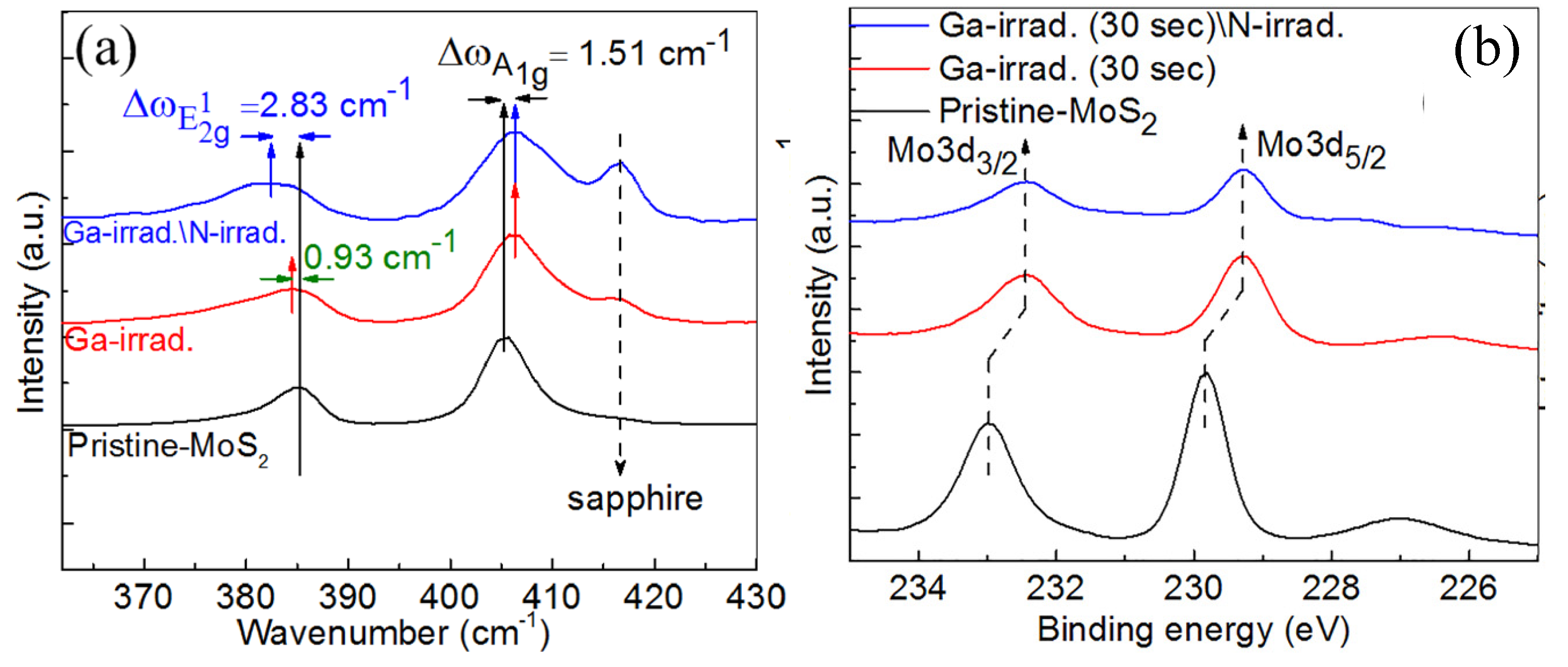
| mono-layer | Ga ion | n/a | n/a | PAMBE | in vacuum | doped Ga, reduced binding energy | [98] |
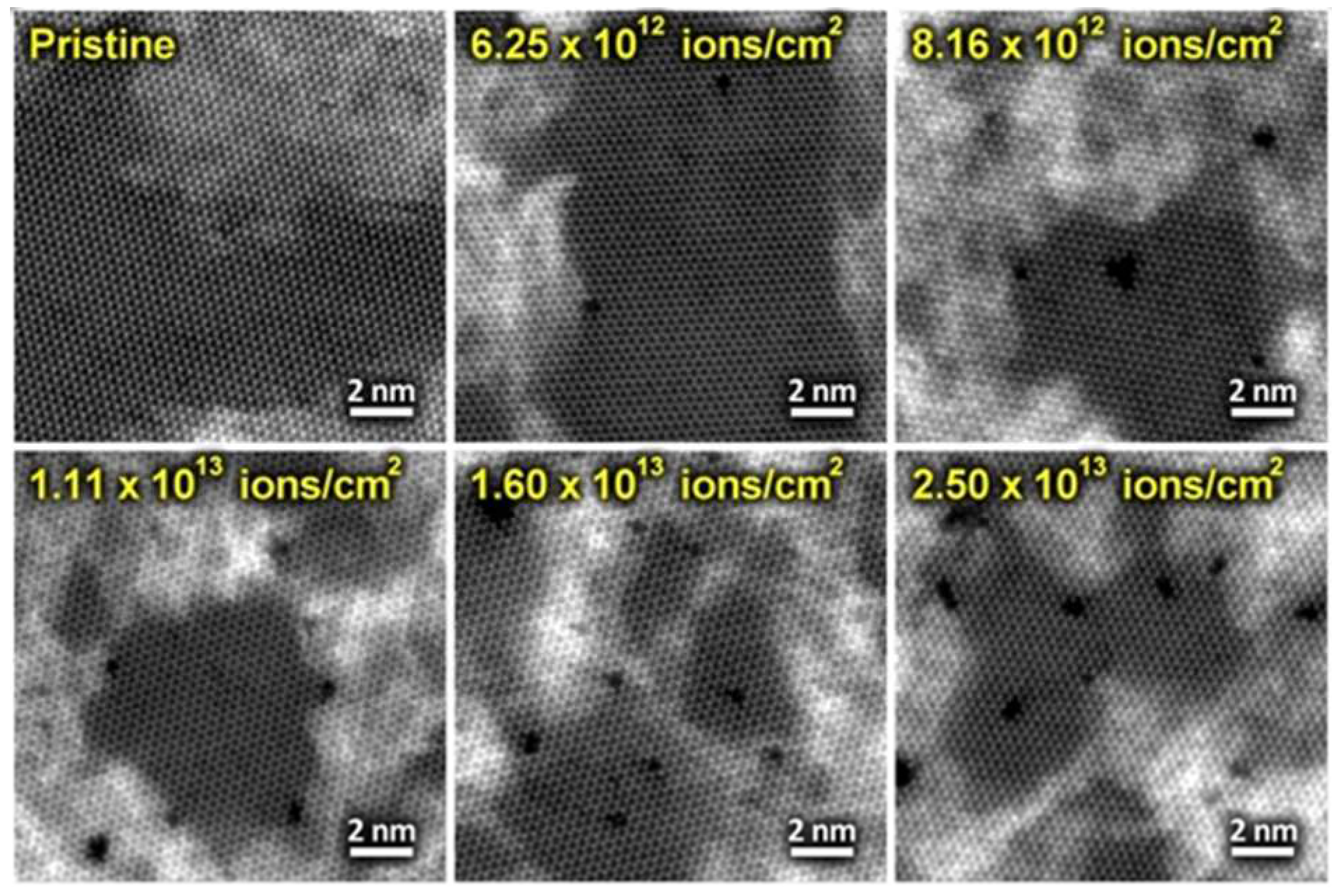
| mono-layer | Ga ion | 30 keV | FIB beam | in vacuum | produced sub-nm pores and vacancies | [99] | |
| bulk | Xe | 91 MeV | GANIL | n/a | formed nano-hillocks | [100] | |
| few-layer | Xe | 91 MeV | GANIL | n/a | formed nano-incisions | [100] | |
| mono-layer | Xe ion | 91 MeV | GANIL | n/a | formed nano-incisions | [100] | |
| mono-layer | Xe ion | 25–30 keV | EBIT | n/a | induced pits and hillocks | [101] | |
| 1–4 layer | Bi ion | 0.45–1.23 | – ions | HIRFL | vacuum, RT | formed hillocks | [102] |
| mono-layer | Mn ion | 25 keV | – ions | TOF-SIMS | UHV | formed defects | [103] |
| bulk | C | 20–40 MeV | – ions | TA | RT | modified structures | [104] |
| micron thickness | -ray | n/a | RGIF | in air | no damaging effects | [105] | |
| 50–132 layer | -ray | 662 keV | 5000 photons | Cs source | RT in air | unaffected | [106] |
| 5–8 layer | -ray | ∼1.2 | Co source | RT in air | converted to MoO | [107] | |
| 1–3 layer | X-ray | 10 keV | 6 Mrad | XRD | RT in air | no noticeable degradation | [108] |
| film | UV | n/a | n/a | mercury lamp | in O (ozone) | formed oxygen-sulfur bonds | [109] |
| mono-layer and multilayer | UV | n/a | – photos | deuterium lamp | vacuum | no structural damage, no oxidation | [110] |
| multilayer | laser | 1–20 mW for 1–100 s | laser | RT in air | stable or damage depending on laser power | [111] | |
| few-layer | laser | diode laser | in air or vacuum | patterned and thinned | [112] | ||
| mono-layer | laser | 20–50 | Ti:sapphire laser | RT | damaged or unaffected depending on irradiation intensity | [113] |
| Comfiguration | Bulk (eV) | Mono-layer (eV) |
|---|---|---|
| single S-vacancy | 14.4 | 5.7 |
| single Mo-vacancy | 24.8 | 18.8 |
| single-line S-vacancy | 39.2 | 30.5 |
| double-line S-vacancy | 66.2 | 62.3 |
| DIV | 28.8 | 23.3 |
© 2019 by the authors. Licensee MDPI, Basel, Switzerland. This article is an open access article distributed under the terms and conditions of the Creative Commons Attribution (CC BY) license (http://creativecommons.org/licenses/by/4.0/).
Share and Cite
Zhao, G.-Y.; Deng, H.; Tyree, N.; Guy, M.; Lisfi, A.; Peng, Q.; Yan, J.-A.; Wang, C.; Lan, Y. Recent Progress on Irradiation-Induced Defect Engineering of Two-Dimensional 2H-MoS2 Few Layers. Appl. Sci. 2019, 9, 678. https://doi.org/10.3390/app9040678
Zhao G-Y, Deng H, Tyree N, Guy M, Lisfi A, Peng Q, Yan J-A, Wang C, Lan Y. Recent Progress on Irradiation-Induced Defect Engineering of Two-Dimensional 2H-MoS2 Few Layers. Applied Sciences. 2019; 9(4):678. https://doi.org/10.3390/app9040678
Chicago/Turabian StyleZhao, Guang-Yi, Hua Deng, Nathaniel Tyree, Michael Guy, Abdellah Lisfi, Qing Peng, Jia-An Yan, Chundong Wang, and Yucheng Lan. 2019. "Recent Progress on Irradiation-Induced Defect Engineering of Two-Dimensional 2H-MoS2 Few Layers" Applied Sciences 9, no. 4: 678. https://doi.org/10.3390/app9040678
APA StyleZhao, G.-Y., Deng, H., Tyree, N., Guy, M., Lisfi, A., Peng, Q., Yan, J.-A., Wang, C., & Lan, Y. (2019). Recent Progress on Irradiation-Induced Defect Engineering of Two-Dimensional 2H-MoS2 Few Layers. Applied Sciences, 9(4), 678. https://doi.org/10.3390/app9040678