Study of Implantation Defects in CVD Graphene by Optical and Electrical Methods

Abstract
Featured Application
Abstract
1. Introduction
2. Materials and Methods
3. Results
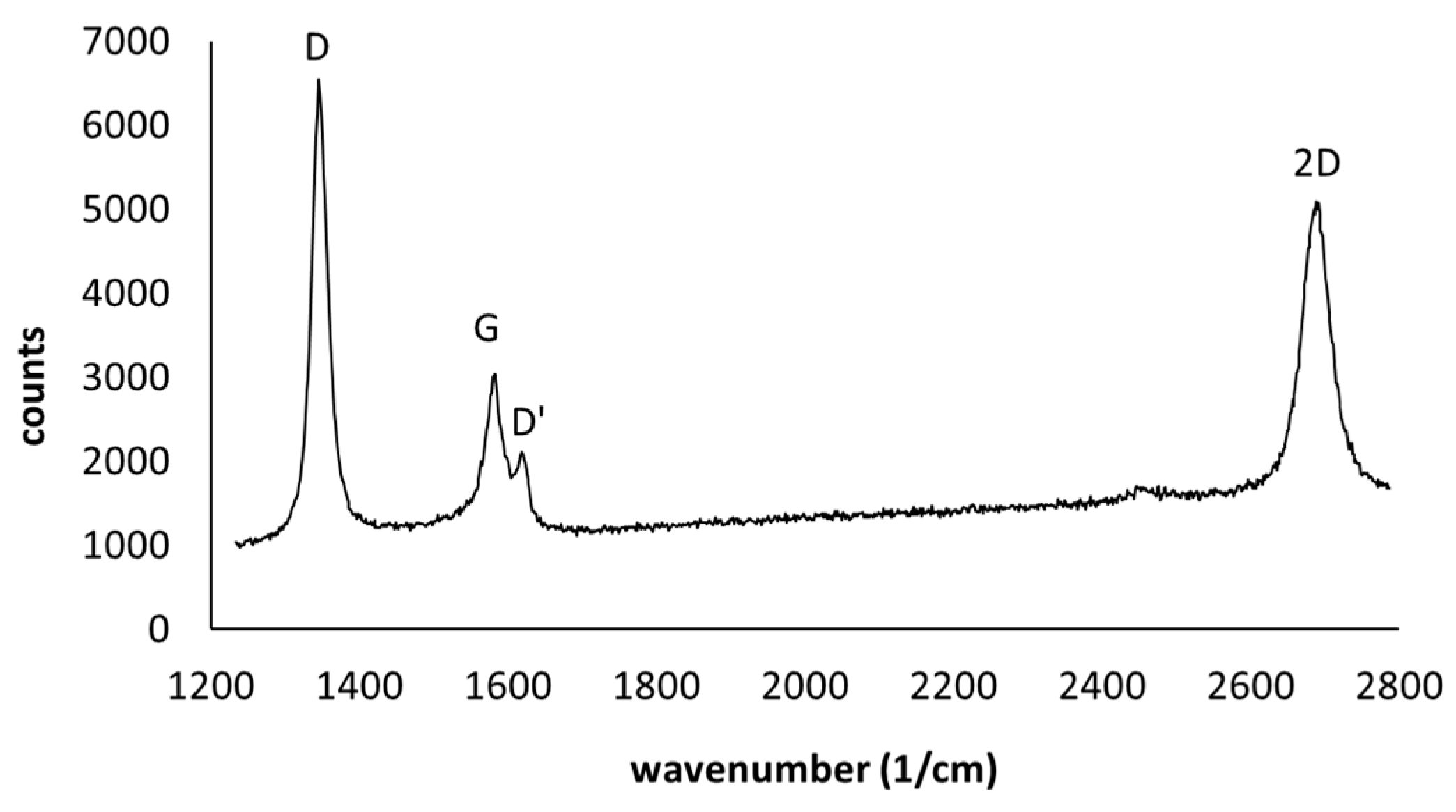
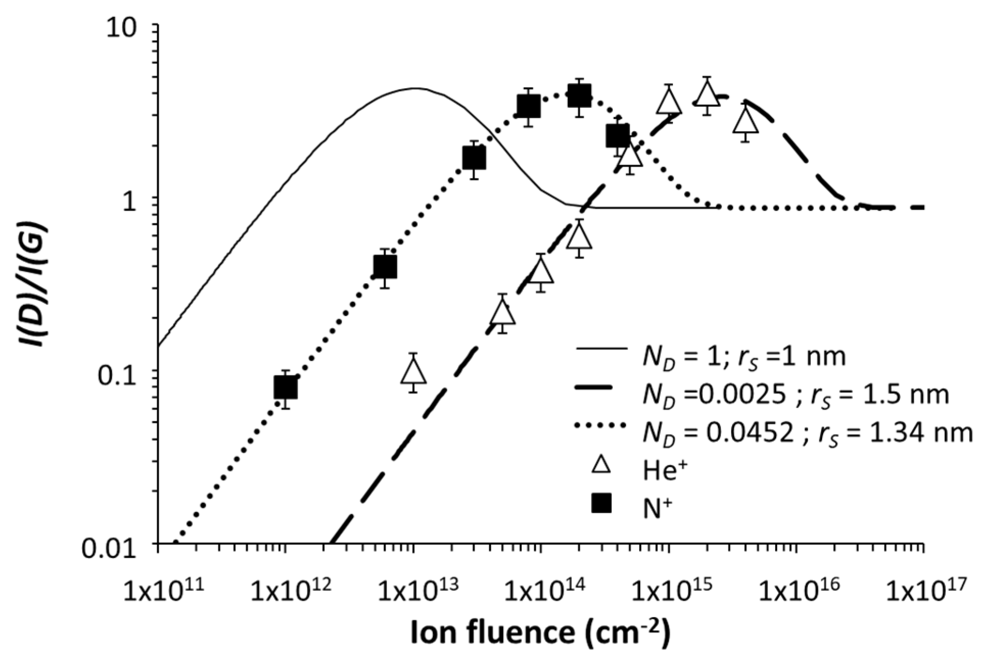
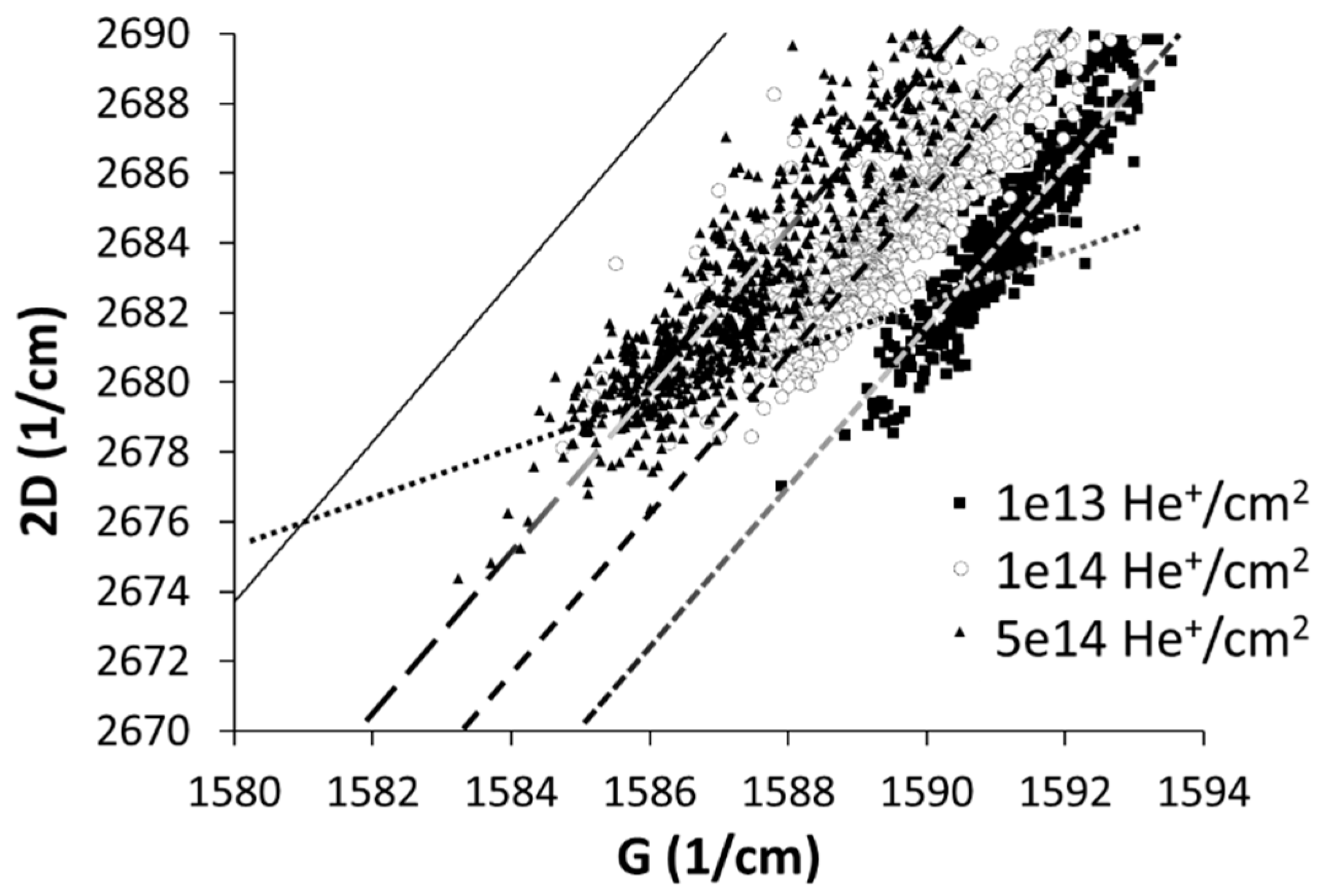
3.1. Raman Measurements
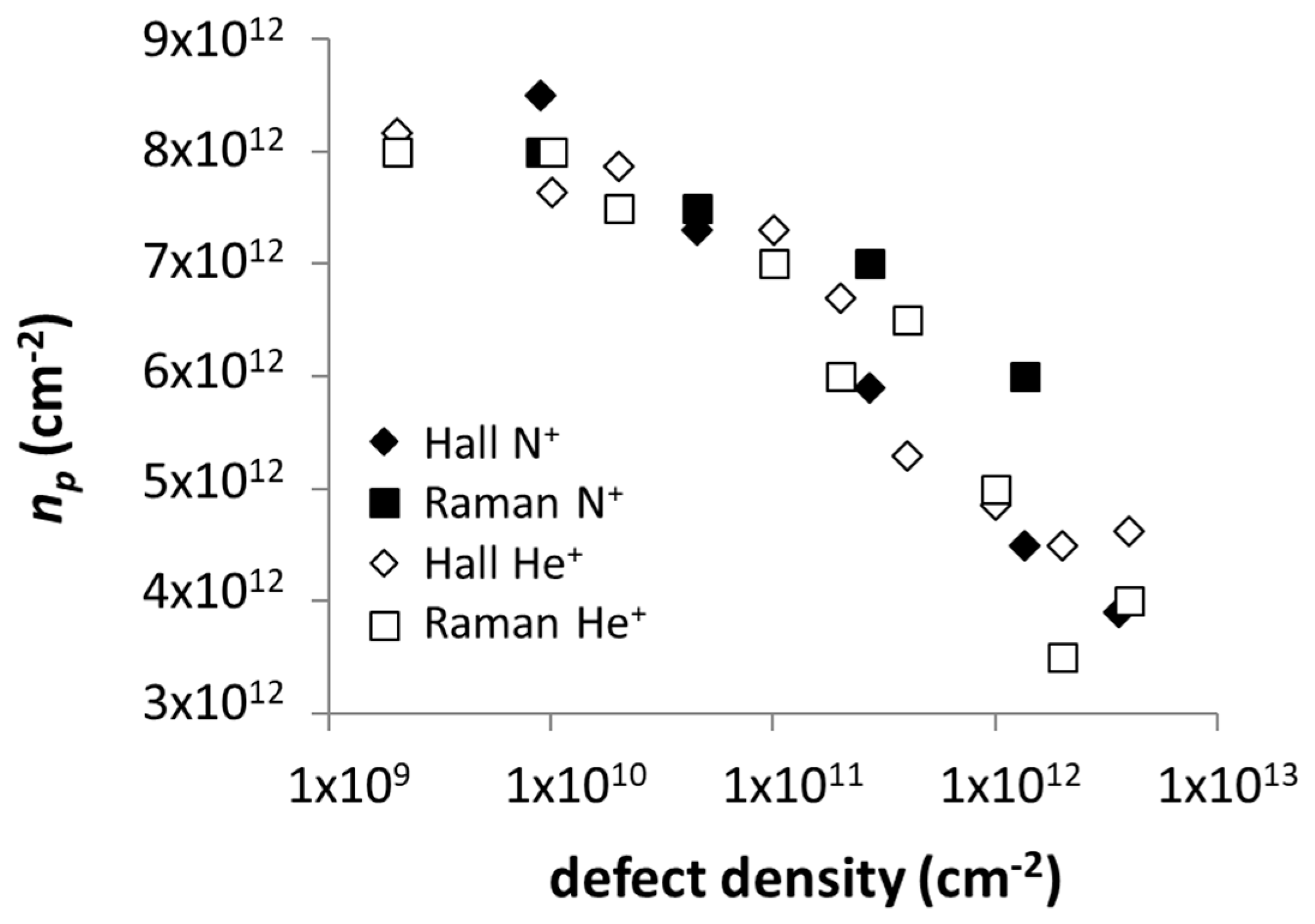
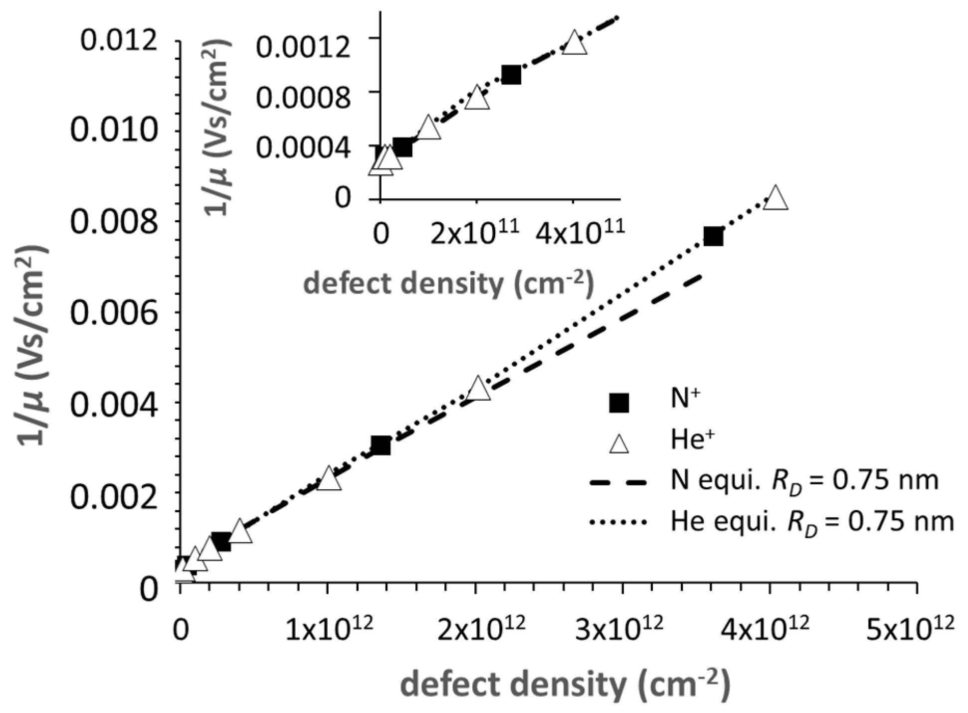
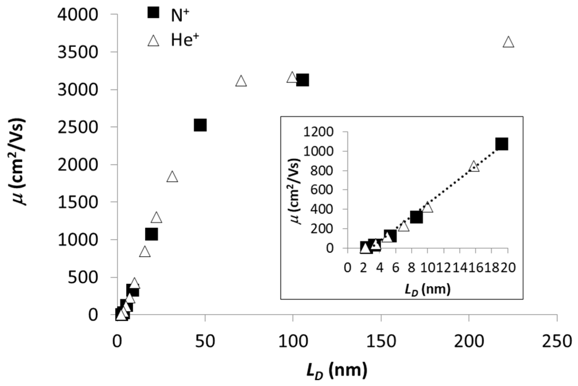
3.2. Electrical Measurements
4. Discussion and Conclusions
Author Contributions
Funding
Acknowledgments
Conflicts of Interest
References
- Ye, J.C.; Charnvanichborikarn, S.; Worslay, M.A.; Kucheyev, S.O.; Wood, B.C.; Wang, Y.M. Enhanced electrochemical performance of ion beam treated 3D graphene aerogels for lithium ion batteries. Carbon 2015, 85, 269–278. [Google Scholar] [CrossRef]
- O’Hern, S.C.; Boutillier, M.S.H.; Song, Y.; Kong, J.; Laoui, T.; Atieh, M.; Karnik, R. Selective ionic transport through tunable subnanometer pores in single-layer graphene membranes. Nano Lett. 2014, 14, 1234–1241. [Google Scholar] [CrossRef] [PubMed]
- Gawlik, G.; Ciepielewski, P.; Baranowski, J.M.; Jagielski, J. Ion beam induced defects in CVD graphene on glass. Surf. Coat. Technol. 2016, 306, 119–122. [Google Scholar] [CrossRef]
- Berger, C.; Song, Z.; Li, X.; Wu, X.; Brown, N.; Naud, C.; Mayou, D.; Li, T.; Hass, J.; Marchenkov, A.N.; et al. Electronic confinement and coherence in patterned epitaxial graphene. Science 2006, 312, 1191–1196. [Google Scholar] [CrossRef] [PubMed]
- Emtsev, K.V.; Bostwick, A.; Horn, K.; Jobst, J.; Kellogg, G.L.; Ley, L.; McChesney, J.L.; Ohta, T.; Reshanov, S.A.; Ruohrl, J.; et al. Towards wafer-size graphene layers by atmospheric pressure graphitization of silicon carbide. Nat. Mater. 2009, 8, 203–207. [Google Scholar] [CrossRef] [PubMed]
- Emtsev, K.V.; Seyller, T.; Speck, F.; Ley, L.; Stojanov, P.; Riley, J.D.; Leckey, R.G.C. Initial Stages of the Graphite-SiC(0001) Interface Formation Studied by Photoelectron Spectroscopy. Mater. Sci. Forum 2007, 556–557, 525–528. [Google Scholar] [CrossRef]
- Emtsev, K.V.; Speck, F.; Seyller, T.; Ley, L.; Riley, J.D. Interaction, growth, and ordering of epitaxial graphene on SiC{0001} surfaces: A comparative photoelectron spectroscopy study. Phys. Rev. 2008, 77, 155303. [Google Scholar] [CrossRef]
- Riedl, C.; Coletti, C.; Iwasaki, T.; Zakharov, A.A.; Starke, U. Quasi-Free-Standing Epitaxial Graphene on SiC Obtained by Hydrogen Intercalation. Phys. Rev. Lett. 2009, 103, 246804. [Google Scholar] [CrossRef]
- Kotakoski, J.; Brand, C.; Lilach, Y.; Cheshnovsky, O.; Mangler, C.; Arndt, M.; Meyer, J.C. Toward two-dimensional all-carbon heterostructures via ion beam pattering single layer graphene. Nano Lett. 2015, 15, 5944–5949. [Google Scholar] [CrossRef]
- Pan, C.-T.; Hinks, J.A.; Ramasse, Q.M.; Greaves, G.; Bangert, U.; Donnelly, S.E.; Haigh, S.J. In-situ observation and atomic resolution imaging of the ion irradiation induced amorphisation of graphene. Sci. Rep. 2014, 4, 6334. [Google Scholar] [CrossRef]
- Robertson, A.W.; Allen, C.S.; Wu, Y.A.; He, K.; Olivier, J.; Neethling, J.; Kirkland, A.I.; Warner, J.H. Spatial control of defect creation in graphene at the nanoscale. Nat. Commun. 2012, 3, 1144. [Google Scholar] [CrossRef] [PubMed]
- Björkman, T.; Kurasch, S.; Lehtinen, O.; Kotakoski, J.; Yazyev, O.V.; Srivastava, A.; Skakalova, V.; Smet, J.H.; Kaiser, U.; Krasheninnikov, A.V. Defects in bilayer silica and graphene: Common trends in diverse hexagonal two-dimensional systems. Sci. Rep. 2013, 3, 3482. [Google Scholar] [CrossRef] [PubMed]
- Gong, C.; Robertson, A.W.; He, K.; Lee, G.-D.; Yo, E.; Kirkland, A.I.; Warner, J.H. Thermally Induced Dynamics of Dislocations in Graphene at Atomic Resolution. ACS Nano 2015, 9, 10066–10075. [Google Scholar] [CrossRef] [PubMed]
- Das, A.; Pisana, S.; Chakraborty, B.; Piscanec, S.; Saha, S.K.; Waghmare, U.V.; Novoselov, K.S.; Krishnamurthy, H.R.; Geim, A.K.; Ferrari, A.C.; et al. Monitoring dopants by Raman scattering in an electrochemically top-gated graphene transistor. Nat. Nanotechnol. 2008, 3, 210–215. [Google Scholar] [CrossRef] [PubMed]
- Strupinski, W.; Grodecki, K.; Wysmolek, A.; Stepniewski, R.; Szkopek, T.; Gaskell, P.E.; Gruneis, A.; Haberer, D.; Bozek, R.; Krupka, J.; et al. Graphene Epitaxy by Chemical Vapor Deposition on SiC. Nano Lett. 2011, 11, 1786–1791. [Google Scholar] [CrossRef] [PubMed]
- Bierwagen, O.; Ive, T.; Van de Walle, C.G.; Speck, J.S. Caused of incorrect carrier-type identification in van der Pauw-Hall measurements. Appl. Phys. Lett. 2008, 93, 242108. [Google Scholar] [CrossRef]
- Ferrari, A.C.; Meyer, J.C.; Scardaci, V.; Casiraghi, C.; Lazzeri, M.; Mauri, F.; Piscanec, S.; Jiang, D.; Novoselov, K.S.; Roth, S.; et al. Raman spectrum of graphene and graphene layers. Phys. Rev. Lett. 2006, 97, 187401. [Google Scholar] [CrossRef]
- Lucchese, M.M.; Stavale, F.; Ferreira, E.H.M.; Vilani, C.; Moutinho, M.V.O.; Capaz, R.B.; Achete, C.A.; Jorio, A. Quantifying ion-induced defects and Raman relaxation length in graphene. Carbon 2010, 48, 1592–1597. [Google Scholar] [CrossRef]
- Lee, J.E.; Ahn, G.; Shim, J.; Lee, Y.S.; Ryu, S. Optical separation of mechanical strain from charge doping in graphene. Nat. Commun. 2012, 3, 1024. [Google Scholar] [CrossRef]
- Mohiuddin, T.M.G.; Lombardo, A.; Nair, R.R.; Bonetti, A.; Savini, G.; Jalil, R.; Bonini, N.; Basko, D.M.; Galiotis, C.; Marzari, N.; et al. Uniaxial strain in graphene by Raman spectroscopy: G peak splitting, Grüneisen parameters, and sample orientation. Phys. Rev. B 2009, 70, 205433. [Google Scholar] [CrossRef]
- Eckmann, A.; Felten, A.; Mishchenko, A.; Britelli, L.; Krupke, R.; Novoselov, K.S.; Casiraghi, C. Probing the nature of defects in graphene by Raman spectroscopy. Nano Lett. 2012, 12, 3925–3930. [Google Scholar] [CrossRef] [PubMed]
- Ochendovski, O.; Lehtinen, O.; Kaiser, U.; Turchanin, A.A.; Ban-d’Etat, B.; Lebius, H.; Karlusić, M.; Jaksić, M.; Schleberger, M. Nanostructuring graphene by dense electronic excitation. Nanotechnology 2015, 26, 465302. [Google Scholar]
- Chen, J.-H.; Cullen, W.G.; Jang, C.; Fuhrer, M.S.; Williams, E.D. Defect Scattering in Graphene. Phys. Rev. Lett. 2009, 102, 236805. [Google Scholar] [CrossRef] [PubMed]
- Ni, Z.H.; Ponomarenko, L.A.; Nair, R.R.; Yang, R.; Anissimova, S.; Grigorieva, I.V.; Schedin, F.; Shen, Z.X.; Hill, E.H.; Novoselov, K.S.; et al. On resonant scatterers as a factor limiting carrier mobility in graphene. Nano Lett. 2010, 10, 3868–3872. [Google Scholar] [CrossRef] [PubMed]
- Buchowicz, G.; Stone, P.R.; Robinson, J.T.; Cress, C.D.; Beeman, J.W.; Dubon, O.D. Correlation between structure and electrical transport in ion-irradiated graphene grown on Cu foils. Appl. Phys. Lett. 2011, 98, 032102. [Google Scholar] [CrossRef]
- El-Barbary, A.A.; Telling, R.H.; Ewels, C.P.; Heggie, M.I.; Briddon, P.R. Structure and energetics of the vacancy in graphite. Phys. Rev. B 2003, 68, 144107. [Google Scholar] [CrossRef]
- Li, L.; Reich, S.; Robertson, J. Defects energies of graphite: Density-functional calculations. Phys. Rev. B 2005, 72, 184109. [Google Scholar] [CrossRef]
- Krasheninnikov, A.V.; Lehtinen, P.O.; Foster, A.S.; Nieminen, R.M. Bending the rules: Contrasting vacancy energetics and migration in graphite and carbon nanotubes. Phys. Lett. 2006, 418, 132–136. [Google Scholar] [CrossRef]
- Lee, G.-D.; Wang, C.Z.; Yoon, E.; Hwang, N.-M.; Kim, D.-Y.; Ho, K.M. Diffusion, coalescence, and reconstraction of vacancy defects in graphene layers. Phys Rev Lett. 2005, 95, 205501. [Google Scholar] [CrossRef]
- Lee, G.-D.; Wang, C.; Yoon, E.; Hwang, N.-M.; Ho, K. Vacancy defects and formation of local haeckelite structures in graphene from tight-binding molecular dynamics. Phys. Rev. B 2006, 74, 245411. [Google Scholar] [CrossRef]
- Miyajima, T.; Tokura, N.; Fukumoto, A.; Hayashi, H.; Hara, K. Nitrogen Ion Implantation and Thermal Annealing in 6H-SiC Single Crystal. Jpn. J. Appl. Phys. 1996, 35, 1231–1234. [Google Scholar] [CrossRef]
- Gaedner, J.; Rao, M.V. Elevated temperature nitrogen implants in 6H-SiC. J. Electron. Mater. 1996, 25, 885–892. [Google Scholar] [CrossRef]


© 2019 by the authors. Licensee MDPI, Basel, Switzerland. This article is an open access article distributed under the terms and conditions of the Creative Commons Attribution (CC BY) license (http://creativecommons.org/licenses/by/4.0/).
Share and Cite
Gawlik, G.; Ciepielewski, P.; Baranowski, J.M. Study of Implantation Defects in CVD Graphene by Optical and Electrical Methods. Appl. Sci. 2019, 9, 544. https://doi.org/10.3390/app9030544
Gawlik G, Ciepielewski P, Baranowski JM. Study of Implantation Defects in CVD Graphene by Optical and Electrical Methods. Applied Sciences. 2019; 9(3):544. https://doi.org/10.3390/app9030544
Chicago/Turabian StyleGawlik, Grzegorz, Paweł Ciepielewski, and Jacek M. Baranowski. 2019. "Study of Implantation Defects in CVD Graphene by Optical and Electrical Methods" Applied Sciences 9, no. 3: 544. https://doi.org/10.3390/app9030544
APA StyleGawlik, G., Ciepielewski, P., & Baranowski, J. M. (2019). Study of Implantation Defects in CVD Graphene by Optical and Electrical Methods. Applied Sciences, 9(3), 544. https://doi.org/10.3390/app9030544