Article

Accurate Constant Phase Elements Dedicated for Audio Signal Processing

Department of Radio Electronics, Faculty of Electronical Engineering and Communications, Brno University of Technology, Brno 616 00, Czech Republic
Appl. Sci. 2019, 9(22), 4888; https://doi.org/10.3390/app9224888
Submission received: 28 July 2019 / Revised: 15 September 2019 / Accepted: 10 November 2019 / Published: 14 November 2019
(This article belongs to the Section Electrical, Electronics and Communications Engineering)

Abstract

:

Featured Application

The proposed constant phase elements are very accurate over audio frequency bandwidth and can be directly utilized in popular and emerging research discipline: design of fractional-order analog building blocks.

Abstract

This review paper introduces real-valued two-terminal fully passive RC ladder structures of the so-called constant phase elements (CPEs). These lumped electronic circuits can be understood as two-terminal elements described by fractional-order (FO) dynamics, i.e., current–voltage relation described by non-integer-order integration or derivation. Since CPEs that behave almost ideally are still not available as off-the-shelf components, the correct behavior must be approximated in the frequency domain and is valid only in the predefined operational frequency interval. In this study, an audio frequency range starting with 20 Hz and ending with 20 kHz has been chosen. CPEs are designed and values tabularized for predefined phase shifts that are commonly used in practice. If constructed carefully, a maximum phase error less than 0.5° can be achieved. Several examples of direct utilization of designed CPEs in signal processing applications are provided.

1. Introduction

Although fractional-order (FO) calculus is an ancient mathematical idea, it has still attracted significant interest from analog design engineers in the last two decades. In the field of signal generation and processing, we can find many applications of FO circuit elements. As mentined in the popularizing paper [1], concepts of circuits with FO elements and with equivalent integer-order parts remain the same, but the system properties and features of the first case can be better. Besided this statement, the author also provides a fundamental background for numerical analysis of FO networks. The application potential of analog circuits with FO elements has been celebrated in a ten year old paper [2], where some possible structures of FO capacitors are described and used in multivibrator circuits. As mentioned, the design of a good FO capacitor is enough ground to start the construction of complex analog FO networks. An FO capacitor can be understood as a two-terminal element that forms a bridge between the resistor and conventional capacitor, which has a module frequency response of admittance linearly increasing with frequency (in a logarithmic frequency scale) slower than the capacitor, and has constant phase shift of current and voltage between 0° and 90°. In theory, these features should be valid from DC up to very high frequencies. Constant phase properties lead to the denotation of FO capacitors as constant phase elements (CPE). In fact, CPE can be understood as a generalization of FO capacitors since the same abbreviation can be used for FO inductors, FO integrators, and other multi-ports. The specific value of a module’s slope and phase shift depends on the mathematical order of an FO element. In the case of FO capacitors, this order could be any real number between zero and one.
Fingerprints that resemble the behavior of true CPEs have been recognized during observations of many physical phenomena in different branches of engineering, including electrical and chemical [3,4,5,6]. Unfortunately, despite huge efforts in the development of suitable materials [7,8] and fabrication techniques [9], “good” FO capacitors that are generally applicable are still not available.
Thus, behavior of CPEs need to be modeled by more complex circuitry with appropriately connected simple components with well-defined dynamics. The first official mention of an electronic approximation of CPEs (in this early stage denoted as fractance or a fractional capacitor) can be found in [10], where impedance (1/s)1/n has been approximated using an RC network. In particular, the case n = 2 is the subject of the paper [11]. Inverse immittance function, that is s1/n, is briefly studied in [12]. Many years later, passive ladder CPE approximations were re-investigated in [13]. Besides generalizations, it is pointed out that these CPEs have close connections to RC networks with distributed parameters. In fact, sections of transmission lines can be used to model the behavior of constant argument impedances. Mathematical descriptions of these CPEs (for example, half-capacitor) can be based on the primary R, G, L, or C parameters per unit length [14]. For lumped realizations of CPE, the author highly recommends two papers [15,16] where the calculation routine of immittance-type passive RC approximants CPEs is described in a step-by-step manner. For a deeper investigation of available CPE approximation techniques, including the popular Chareff and Oustaloup methods, readers should consult a comprehensive review [17]. This paper provides advice and formulae how to choose the optimal order of passive RC approximation circuits.
Considerable attention was paid to active implementations of CPE. Complex immittance-type CPEs that take advantage of the multiplication of many first-order zero-pole immittances are thoroughly investigated in [18]. Electronic tunability (via external DC signals) of the trans-conductances associated with voltage-controlled current-sources can be used to set the phase shift of CPE approximation, as pointed out in [19]. However, since trans-conductances vary with temperature and age, sensitivity issues need to be addressed. From a practical point of view, the cascading of simple bilinear sections based on AD844 integrated circuits could be a better active solution for CPEs [20]. Because a pair of bilinear filters can be interchanged by a general biquadratic section, two-port CPEs can be approximated using second-order filters [21]. Comparative studies of active realizations of both impedance-type and admittance-type two-terminal CPE approximants can be found in [22]. A similar analysis of different active implementations of two-port CPEs is the topic of [23]. A change of the trans-conductance of operational trans-conductance amplifiers can be used to change the FO nature of a two-terminal element. This idea was first introduced briefly in [24], and, considering one active alternative, developed into complete circuitry described in detail in [25].
CPEs have been advantageously incorporated into many different building blocks of analog signal processing. First, let us discuss a few applications of CPE in the signal generation process. The most straightforward approach to how FO oscillators can be obtained is by direct replacement of capacitors or inductors with an FO equivalent. This works well for the common structures of feedback oscillators [26], oscillators based on integrator block schematics [27], as well as for oscillators based on state variable circuit synthesis [28]. However, detailed study of these and similar publications reveals that such a substitution does not bring significant benefits over conventional integer-order harmonic oscillators. Moreover, in the case of the negative resistance concept of an oscillator, the negative slope of the nonlinear component needs to be adjusted; a linear sub-circuit is “more stable” since the roots of the describing characteristic polynomial have different locations in complex planes (see [29] for clarification). Probably the most promising advantage of employing FO elements inside a generator of harmonic waveforms can be noticed in the multi-phase oscillators [30] or electronically adjustable oscillators with a constant phase shift between two circuit nodes over the whole tunability range. Note that the second case can be implemented by using two integer-order all-pass filters in a cascade; only the control of frequency change becomes much more complicated (additional circuitry needs to be included). The author highly recommends [30] because it can be considered as a cookbook for designers of FO oscillators. Circuit elements with FO dynamics can be utilized also to enhance the behavior of relaxation oscillators. Easy replacement of a common capacitor with an FO equivalent can generate time domain waveforms [31] that make use of a memory property (oil-like effect).
The second area, where many sound applications, discoveries, and interesting publications can be found, is signal processing. Although fractionality can be introduced into continuous-time as well as discrete-time dynamic systems, let us focus on the linear continuous-time systems, starting with frequency filters with CPEs. The simplest ideas, including transfer functions and associated frequency responses of the first-order filters generalized to FO domains, are presented in [32]. Since this interesting work describes the behavior of a near zero-order filter under idealized conditions, it also serves as a springboard for many upcoming studies, research papers, and applications. Much more versatile transfer functions in the Laplace transform, leading to a large variety of frequency responses, are provided in [33]. Therein, analog frequency filters with a total order between one and two are addressed. Theoretical analysis of low-pass filters, both with hand-made and electronically adjustable significant frequencies and quality factors, is the subject of [34,35,36]. Similarly, FO high-pass filtering structures is the topic of [37]. However, network structures proposed here can be considered as standard, with direct replacement of all capacitors with FO immittance equivalents. The presented results, i.e., frequency responses and filter parameters, do not exhibit significant benefits. Several different reconfigurable FO filters, i.e., multi-ports with different accessible frequency responses, can be found in [38,39,40,41]. In these publications, reaching different slopes seems to be the focus of authors. Specific classes of the so-called (1 + α) filters, i.e., circuits having a mathematical order between one and two, are thoroughly studied in [42,43]. The network presented and analyzed in [44] also belongs to this class of filter, but allows for full adjustment of the filter’s quality factor. This useful feature can be incorporated into the standard configuration of the Kerwin-Huelsman-Newcomb (KHN) filter, but at the cost of an additional active element connected as an amplifier. Synthesis and analysis of the higher-order FO filters is thoroughly discussed in [45]. The design process of active filters (including those with FO elements) can be significantly sped up by using a field programmable analog array (FPAA) [46,47]. Besides the necessary frequency limitations of these development kits (defined by intrinsic low-pass filters), there is also a restricted area dedicated to circuit design. Thus, only simple active topologies can be implemented using an FPAA. An interesting question is the correct operation and network topology leading to an FO all-pass filter. The simple interchange of common accumulation elements with an FO equivalent does not lead to a module frequency response that is constant and independent of frequency. This problem has been recognized, and the authors of [48] tried to solve it with only partial success, since the module frequency response is not flat. CPEs are core circuit elements in a class of building blocks where the module frequency response is not as important as the phase frequency response. Asymptotical phase shifters are devoted to the phase transition between two arbitrary values for frequency, moving from DC to infinity. There are two related types with increasing [49] and decreasing [50] phases. The core idea behind both papers is to practically realize predefined complex transfer functions as a composition of a simple (order is equal to or less than unity) sub-parts. This is a task suitable for cascade synthesis. Individual two-port sections can be, for example, implemented by a sequence of inverting amplifiers connected in a common configuration with voltage-feedback operational amplifiers and grounded non-inverting inputs. The only condition is a sufficiently large value of input impedance for each section. This input impedance corresponds to the module of impedance connected to the input terminal. Of course, there are other possibilities for implementing high-input impedance voltage-mode two-port configurable transfer functions.
The design of modern feedback regulators has been intentionally affected by the presence of an FO element, either two-port or two-terminal. Differences and similarities of integer-order and FO Proportional-Integration-Derivation (PID) control is discussed in [51]. The reason for this is to avoid abrupt changes in the dynamics of plant processes [52,53], or due to the necessity of gaining smooth control of the derivation and integration process. FO circuit elements are included in the single-input single-output configurations of PID regulators (see tutorial [54]). Therein, a few interesting examples of the very fast processes that are successfully controlled, and the corresponding measured responses, are provided. The design of PID controllers for fractional-order systems with time delays is presented in [55]. FO feedback control of DC motors is the subject of [56]. The properties of common structures of the integrated voltage regulator were studied in [57]. Therein, a passive RC approximant located in a closed feedback loop significantly improved the performance of a designed regulator, as documented by circuit simulations. FO elements can find useful applications in DC–DC converters, as recognized by authors of [58]. This paper illustrates a promising method for analysis of FO DC–DC converters demonstrated on boost converters working in continuous conduction mode. The same operational regime, but a general class of DC–DC converters (buck, boost, and buck–boost), is assumed in the case of the investigations presented in [59]. Therein, the authors include an FO inductor in the standard topology of converters. This is motivated by non-idealities in large commercial inductors, i.e., the necessity to obtain a better model and more accurate results.
To this end, the modeling of real physical phenomena, where descriptive information is usually available as measured data sequences, by using FO differential equations can be observed in many other research fields. FO wireless power transmission systems are shown in paper [60]. Wideband CPEs need to be utilized while studying chaotic dynamics with the lowest possible order [61] if new FO systems with robust strange attractors are to be discovered [62], or if FO circuit elements should be working in wideband applications such as FO memristors in generators of chaotic waveforms based on Wien bridge oscillator topology [63].
Shortcomings, which have been recognized in many papers focused on the utilization of FO elements in analog systems, are based on frequency limitations of CPE approximants. In other words, CPEs keep a predefined phase shift only in the finite frequency bandwidth (with a top and bottom boundary), and this should be respected by circuit designers and developers of applications. Unfortunately, this limitation is a source of the functional errors in many papers published in renowned journals. For example, many “fractional-order” filters proposed in the literature can be hardly utilized in real situations, since correct operation is restricted to two frequency decades of processed signals. This is especially obvious in the case of FO frequency filters. Some authors adopt FO sub-circuits that work well only within one, two [64], or, at most, three decades [65,66] with significant phase corrugation. Generators of the harmonic signals are not demanding applications with respect to CPEs unless these are supposed to be tunable in a wide frequency range. Thus, the CPEs utilized in [67] cannot be transferred to other systems that oscillate at a different frequency.
This paper is organized as follows: Section 2 describes the different possibilities for lumped circuit realization of CPEs. Individual types of circuits are equivalent in the sense that any phase shift between 0° and 90° can be realized. Section 3 details fully passive RC implementations of CPEs, including numerical values of the circuit components and error analysis, calculated in Mathcad. Section 4 of this work discusses a few practical applications of audio CPEs; introduced two-port phase shifters can perform non-asymptotical phase shifting, i.e., connect two arbitrary points on the phase frequency response. Furthermore, a bass-corrector and a subsonic voltage-mode two-port with arbitrary constant phase shift is designed. Section 5 is devoted to discussion; several problems with CPEs are revealed and solutions are suggested. Finally, concluding remarks and possible future research topics are provided.

2. Passive and Active Structures of CPE Approximants

So far, from the viewpoint of practical applications in lumped analog signal processing, the passive RC ladder structure of CPE approximation appears to be the most promising concept. The advantages are evident: passivity (CPEs without a supply voltage), straightforward understanding, simple frequency and impedance rescaling, easily calculated numerical values of the internal circuit components, non-laborious practical implementation, and verification. The authors of [15,16] provide systematic design approaches and complete calculation routines. There are four input parameters: required phase shift (the order of CPEs to be approximated multiplied by 90°), phase error (defines the width of the canal where the phase frequency response will unfold), frequency band (where the predefined phase error will be kept), and basic immittance constant (changes the pseudo-capacitance if the FO capacitor is designed). The order of CPE approximation circuits is a compromise between the first three input parameters; this statement will be clarified in upcoming text.
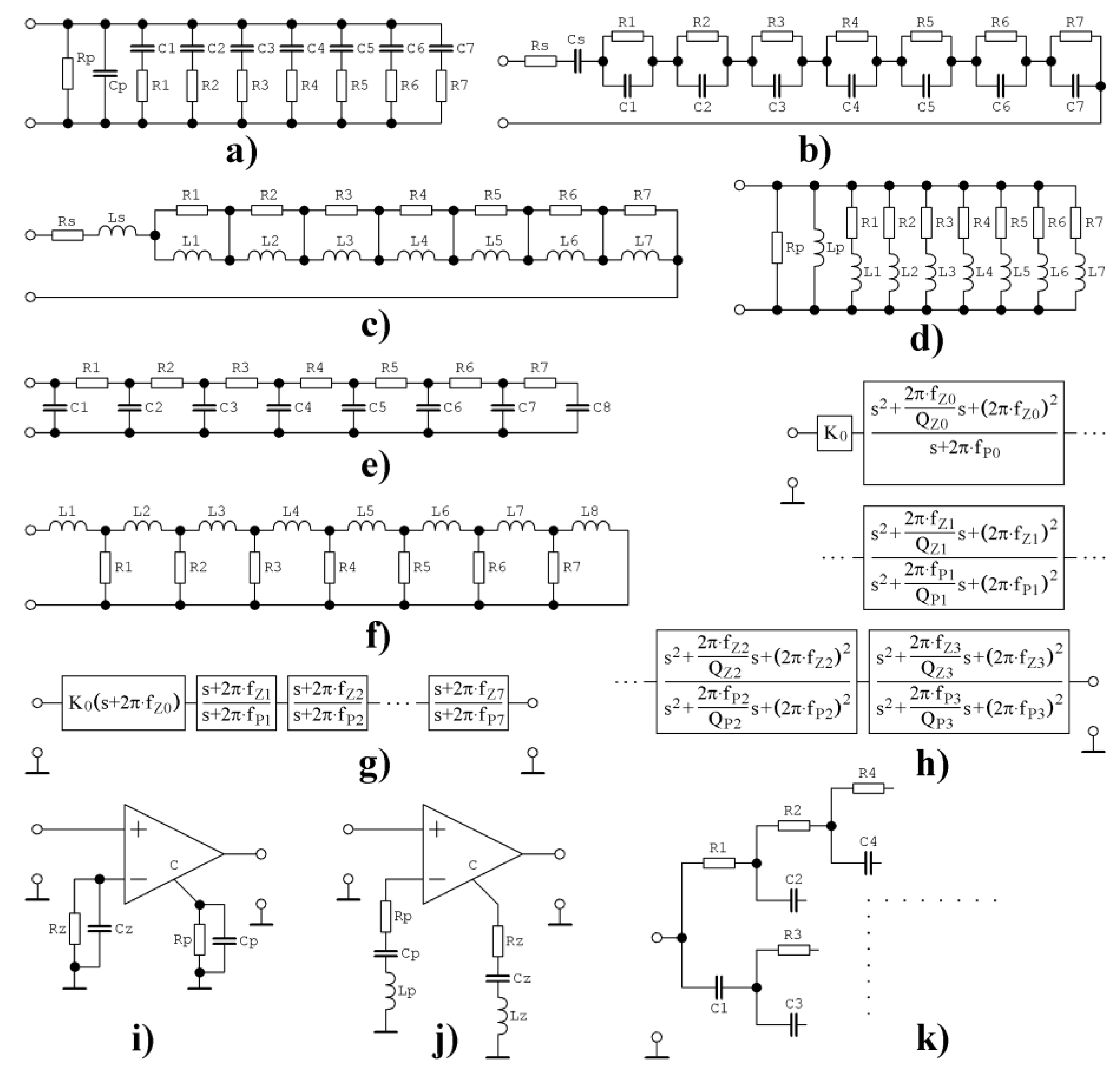
First, and the most popular, two-terminal realization of CPEs is visualized by means of Figure 1a and described by the following function in Laplace transform
Y ( s ) = I ( s ) V ( s ) = s C p + 1 R p + k = 1 7 s C k s C k R k + 1 = s C p + 1 R p + k = 1 7 1 R k · s s + ω k ω k = 1 C k R k ,
where s is complex frequency. The sum indicated in (1) de facto represents the complex admittance function decomposed into the partial fractions. Hence, CPEs with a math order less than one will be substituted by a circuit with total order eight. Because of the topology, this RC circuit will be denoted in further text as a series-parallel structure.
An alternative circuit suitable for CPE approximation is provided in Figure 1b, and can be described by the following network functions
Y ( s ) = I ( s ) V ( s ) = 1 R s + 1 s C s + k = 1 7 R k s C k R k + 1 Z ( s ) = V ( s ) I ( s ) = R s + s L s + k = 1 7 s L k R k s L k + R k .
Again, the sum in (2) can be interpreted as the decomposition of complex impedance functions into partial fractions. Because of the internal topology, this RC circuit will be referred in this paper as a parallel-series structure.
Both network structures presented above can be used in voltage-mode as well as current-mode applications. Furthermore, both admittances can be transformed into impedances (admittance function has the same form as impedance function) by following the duality principle. Corresponding schematics are given in Figure 1c,d. This paper provides only realizations of FO capacitors. To obtain FO inductors, capacitors should be substituted for inductors (with the same normalized value), resistors interchanged with conductors (that is, resistors having inverse normalized values), and the parallel connection of components connected in series and vice versa. The behavior of the FO inductor provided in Figure 1c in the frequency domain can be approximated by the function
Z ( s ) = V ( s ) I ( s ) = s L s + R s + k = 1 7 s L k s L k / R k + 1 = s L s + R s + k = 1 7 R k · s s + ω k ω k = R k L k ,
and the FO inductor depicted in Figure 1d is described by the function
Z ( s ) = 1 Y ( s ) = V ( s ) I ( s ) = 1 1 / s L p + 1 / R p + k = 1 7 1 s L k + R k .
Now, let us discuss general properties of the network functions (1)–(4). Each immittance function of the CPE approximant can be expressed in form as a rational fraction
F ( s ) = k = 0 n a k s k k = 0 m b k s k ,
where n and m are natural numbers (with unity maximal difference) and ak and bk are real positive constants, or equivalently as
F ( s ) = a n b m · k = 1 n ( s + ω Z k ) · k = 1 m 1 s + ω P k ,
where ωZk and ωPk are the so-called zeroes and poles of the network function F(s). Note that zeroes and poles are supposed to be real numbers. Moreover, these zeroes and poles are singular, located on the horizontal axis of the open left half-plane of complex planes, and alternates with respect to frequency. The corresponding phase frequency response can be written as
φ ( ω ) = k = 1 n a t a n ω ω Z k k = 1 m a t a n ω ω P k .
As is known from the theory of filters, each zero causes a smooth 90° positive contribution to phase shift, while each pole causes the same, but negative, contribution—a −90° phase shift. Thus, the appropriate deployment of zeroes and poles (the values of angular frequencies ωZk and ωPk) can lead to a symmetrical phase ripple around any value in the range −90° to 90°. There are three important consequences coming from this kind of CPE approximation, and all should be respected within their intended applications. Firstly, CPE approximation is valid only in a finite frequency range. Secondly, the phase frequency response is no longer constant—it is rippled around a predefined value. The module frequency response is not a straight line—it has a stair-like shape. Furthermore, for small phase errors, zeroes and poles need to be located close to each other. Additional zeroes and poles always mean a more complicated final circuit structure of the CPE approximant. Finally, there is always a tendency to keep the order of CPE approximation circuits as low as possible because the mathematical order of a designed functional block (where CPE is incorporated) is increased by this number.
Now, let us summarize the properties of CPEs that we need for audio applications. The frequency band begins with 20 Hz and stops at 20 kHz, and a predefined maximal phase deviation within this interval should be 0.5°. Computer analysis and practical experiments supported by the formula provided in [17] returns the required number of seven RC sections regarding Figure 1a,b. Namely, the admittance function of the circuit in Figure 1a has eight zeroes (n = 8) and seven poles (m = 7), and approximation begins and ends with zero. At low frequencies, the phase shift starts to increase, and in the operational frequency range, zero–pole interactions take place, and approximation ends with a high frequency zero. Thus, phase shift asymptotically reaches 90° for high frequencies. Remember, for very high frequencies, the RC ladder network can no longer be considered as a circuit with lumped parameters. Straightforward analysis of the second network connection provided in Figure 1b gives the same number of zeroes and poles of complex impedance, m = n = 8. Series capacitor Cs leads to the first zero ωk1 = 0. Consequently, phase shift asymptotically returns to zero for frequencies above the approximated range. This property can be important regarding the stability of the electronic system.
General Expression (6) represents a cascade connection of m + n fundamental network functions. For any combination of two zeroes and two poles, a cascade of the bilinear network functions can be rewritten into the product of biquadratic network functions, i.e.,
F 1 ( s ) = a 8 b 7 · s 2 + ω Z 7 ω Z 8 Q Z 4 s + ω Z 7 ω Z 8 s + ω P 7 · k = 1 3 s 2 + ω Z ( 2 k 1 ) ω Z ( 2 k ) Q Z k s + ω Z ( 2 k 1 ) ω Z ( 2 k ) s 2 + ω P ( 2 k 1 ) ω P ( 2 k ) Q P k s + ω P ( 2 k 1 ) ω P ( 2 k ) ,
where the quality factor associated with a pair of zeroes, ω1 and ω2, (or poles) is Q = √ (ω1·ω2)/(ω1 + ω2) For real zeroes and poles with significant distances, we reach very low-quality factors, much lower than Q = 1/2. Note that network function F1(s) is related to the RC approximation given in Figure 1a. The second structure has a similar decomposition, namely
F 2 ( s ) = a 8 b 7 · s ( s + ω Z 7 ) s 2 + ω P 7 ω P 8 Q P 4 s + ω P 7 ω P 8 · k = 1 3 s 2 + ω Z ( 2 k 1 ) ω Z ( 2 k ) Q Z k s + ω Z ( 2 k 1 ) ω Z ( 2 k ) s 2 + ω P ( 2 k 1 ) ω P ( 2 k ) Q P k s + ω P ( 2 k 1 ) ω P ( 2 k ) .
Significant frequencies and quality factors of zeroes and poles of CPEs depend on the choice of coupled zero pairs and pole pairs (this choice can be arbitrary). A low quality of zeroes and poles means that the individual cells of two-port approximation can be realized by the RC-only circuits, for example, by using the tree structure shown in Figure 1k, bridge-T network, etc.
Next, the RC network structure in Figure 1e can be considered as a single-ended finite (but long enough for good approximation) transmission line divided into cells, each cell being described by two out of four primary parameters. The corresponding admittance function can be written as the continued fraction
Applsci 09 04888 i001
Because of the long and very complex expression for individual coefficients of the polynomials of Ratio (5), Admittance (5) and (6) will not be provided in this form. However, Admittance (10) can be rewritten using the matrix method of unknown nodal voltages as
Y ( s ) = I ( s ) V ( s ) = d e t ( Y ) d e t ( Y 1 , 1 ) Y = ( s C 1 + G 1 G 1 0 G 1 s C k + G k 1 + G k G k 0 G k ) ,
where Y is determinant of the admittance matrix, Y1,1 is sub-determinant after remov its first row, column k = 2, 3, …, 8 is the index of independent nodes, and Gk = 1/Rk. Admittance matrix Y is terminated by the element y88(s) = sC8 + G7.
By the principle of duality, we can construct a single-ended finite transmission line composed of the two remaining primary parameters as demonstrated in Figure 1f. The impedance function of this complex two-terminal element can be expressed as
Applsci 09 04888 i002
Similarly, as it is in the case of admittance, Complex Impedance Function (12) can be expressed as ratio of determinant Z and sub-determinant Z1,1 after removal of the first row and column
Z ( s ) = V ( s ) I ( s ) = d e t ( Y 1 , 1 ) d e t ( Y ) Y = ( 1 / s L 1 1 / s L 1 0 1 / s L 1 1 / s L k 1 + 1 / s L k + G k 1 1 / s L k 0 1 / s L k ) ,
where k = 2, 3, …, 8 is the index of independent nodes and Gk = 1/Rk. In this case, admittance matrix Y is terminated by the element y88(s) = 1/sL8 + G7. The numerical values of k-th transmission line cell Ck, Gk, and Lk can be obtained by an optimization routine.
Two-port circuitry realizations of CPEs based on the locations of zeroes and poles of the network function (voltage-mode, current-mode, trans-impedance-mode, or trans-admittance-mode) are given symbolically in Figure 1g. The required configuration of zeroes and poles of the final voltage transfer function can be constructed by using a cascade of the bilinear filters. A huge number of available topologies can be found via the internet. One promising active implementation of voltage-mode two-port using direct knowledge of the locations of zeroes and poles is provided in Figure 1i. The values of capacitors CZ and CP in one active cell predefine the frequency decade where the zero-pole pair is placed (high C means low f and vice versa). The advantage of this concept is obvious: these bilinear filters have a very simple relationship between circuit components and Voltage Transfer Function (6).
As mentioned above, biquadratic filters can also be utilized to model CPEs if they are placed in a cascade. Both band-pass and band-reject filters can be used. The decomposition of voltage transfer function F1(s), i.e., Formula (8), is visualized in Figure 1h, where K0 = a8/b7. A slight modification of the branch impedances in Figure 1i leads to two-port realization where a significant frequency and quality factor are the key parameters (see Figure 1j). Alternative modifications with parallel resonant sub circuits also lead to suitable forms of voltage transfer function. Inside both cells, a commercially available integrated circuit AD844 (a second generation current conveyor followed by a voltage buffer) is utilized. The second circuitry can be considered as a single-band audio equalizer. The voltage transfer function of these cells can be expressed as follows
K ( s ) = V o u t V i n = C Z C P · s + 1 / ( R Z C Z ) s + 1 / ( R P C P ) K ( s ) = V o u t V i n = L Z L P · s 2 + R Z L Z · s + 1 L Z C Z s 2 + R P L P · s + 1 L P C P .
Note that for both circuits given in Figure 1i,j, the locations of zeroes and poles are independently and uniquely determined by values of the passive circuit components. Quality factors associated with series resonant circuits are very low, such that a synthetic grounded inductor can be used. Synthetic lossy inductors are also supposed to be used in the case of the implementations provided in Figure 1c,d. There are many network topologies that can emulate very large values of self-inductance. For example, Prescott’s topology is simple (one or two operational amplifiers are needed for the simulation of grounded and floating inductors, respectively) and can be used for large self-inductance at the cost of large resistance in the series. Antoniou’s structure utilizes two (grounded inductor) or four (floating inductor) operational amplifiers, and can model very large self-inductance with negligible resistance in series.
In the Orcad Pspice circuit simulator, CPE two-ports can be emulated using a cascade of LAPLACE blocks. Both transfer functions from (12) can be, with appropriate numerical values of coefficients, written directly to a numerator and denominator and simulated via an AC sweep. Following this concept, we can study the influence of individual coefficients to the module and phase frequency response of CPEs, i.e., judge sensitivities. The quality of CPE approximation can be quantified with respect to many aspects, including user-defined figures of merit. However, the standard measure is the absolute error accumulated over the desired frequency range, i.e., by definite integral
ε = f 1 f 2 a b s ( k = 1 n a t a n ω ω Z k k = 1 m a t a n ω ω P k π 2 α ) d f ,
where ωZk and ωPk are the positions of the k-th zero and pole, respectively, and α is order of the CPE. Using this, sensitivities can be considered as a degree of displacement of individual zeroes and poles with respect to some circuit components.

3. Approximation of CPE in Frequency Domain and Numerical Results

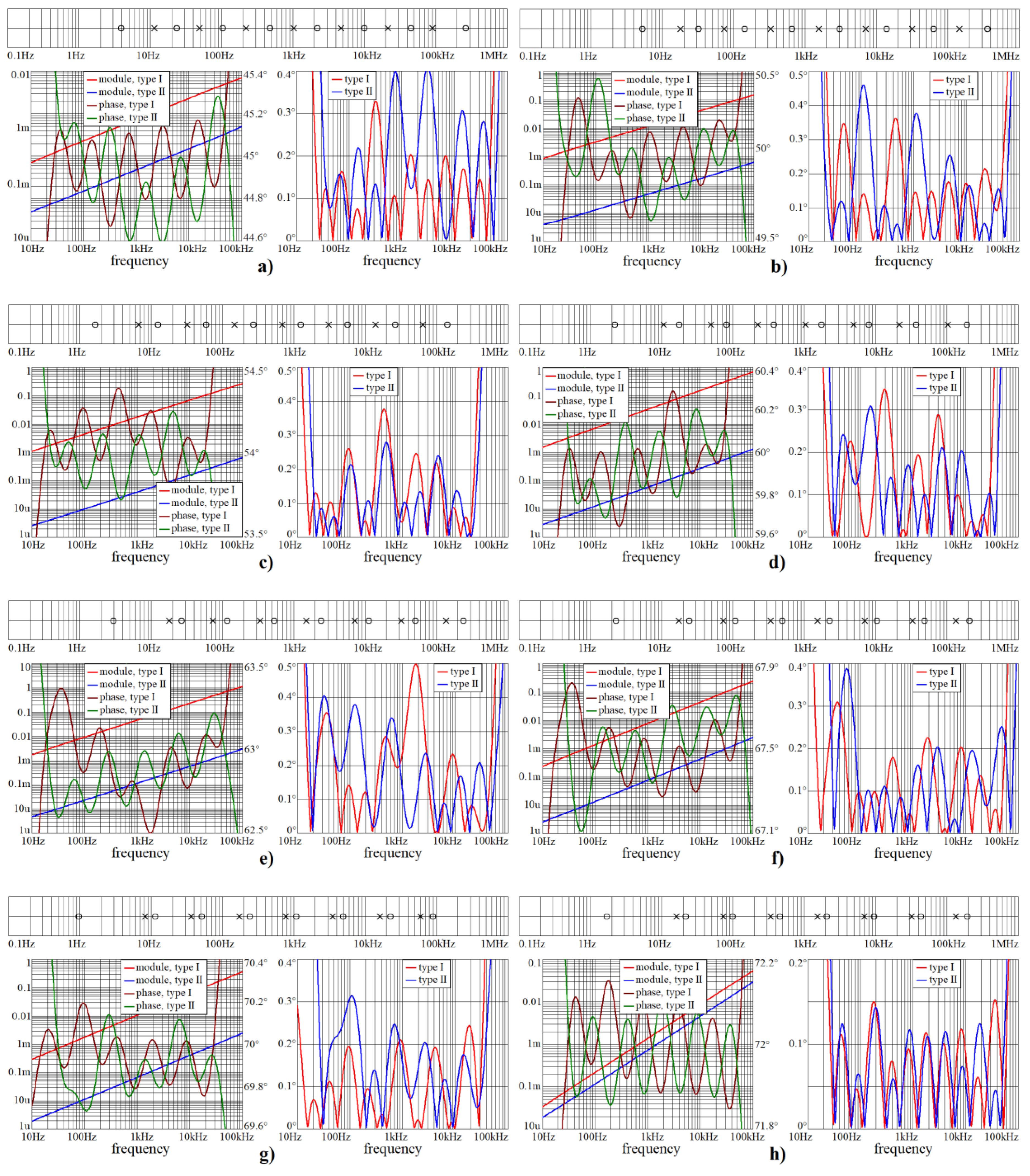
Upcoming subsections show detailed numerical results associated with CPE approximants for individual mathematical orders. These subsections are sorted from the lowest value of order (1/10) and ends with the highest value (9/10). All designed CPEs for demanding audio applications have a very small phase error—lower than 0.5°, and in some cases even lower than 0.2°. This section continues with the design of CPEs that are provided in a sequence given in ascending order of CPE. Firstly, audio CPEs are provided in Section 3.1, Section 3.2, Section 3.3, Section 3.4, Section 3.5, Section 3.6, Section 3.7, Section 3.8, Section 3.9, Section 3.10, Section 3.11, Section 3.12, Section 3.13, Section 3.14, Section 3.15, Section 3.16, Section 3.17, Section 3.18 and Section 3.19. Graphical visualizations of numerical verification of designed CPEs are the subject of Section 3.20. To create as universal a range of CPEs as possible, quarters, and decimal mathematical orders of approximants, as well as elements with 10° phase shift steps, are considered. A complete list of designed CPEs is provided in Table 1. Figure 2 shows selected results for audio CPEs.
Fundamental properties of two-terminal CPEs form headers of the subsections such that desired realization (phase shift) can be easily found. In upcoming tables, the symbols ∠ and‖ denote series and parallel connection of passive circuit components, respectively. Considering the E12 value series only, parallel combinations of circuit components are preferred due to the lower sensitivities. Of course, the denser fabrication series of the passive components, such as E24 and E48, can be also used. However, different values for the passive components do not provide much better results (more accurate CPE approximation). For CPEs with as low phase errors as announced in this paper, the precision of the final CPE product in practice depends on the diligence and manual skills of the engineer.
The FO nature of ideal two-terminal admittance can be expressed in form Y(s) = Y0·sα, where Y0 is the so-called pseudo-capacitance. It is, de facto, a module of admittance| Y()| measured at the angular frequency 1 rad/s. Such a frequency is out of range for audio CPEs. Thus, the module frequency response was linearly extrapolated (in the log-scaled axis system) to obtain this roughly estimated measure. The so-called pseudo-inductance Z0 is calculated using an analogical approach, and is bounded to ideal expression for the FO impedance Z(s) = Z0·sα. Besides numerical values of directly calculated resistors and capacitors (normal font), a suitable series-parallel interconnection is presented (bold letters). Of course, it is not unique, but it represents the best choice as thoroughly verified by AC analysis in Orcad Pspice circuit simulator. Neither values of coefficients of numerator and denominator of Fraction (5) nor Decomposition (6) are provided; these can be easily calculated using a suitable mathematical tool such as Matlab or Mathcad.

3.1. Audio CPE for Mathematical Order α = 1/10, Prescribed Phase Shift φ = ±9°

This CPE begins with frequency f0 = 1/(2πR0C0) = 1/(2π·5·104·10−6) = 3.2 Hz and the impedance constant is 103. Numerical values are given in Table 2 and Table 3, and pseudo-capacitance is 2.044 mF/s9/10 (type I) and 1.985 mF/s9/10 (type II).

3.2. Audio CPE for Mathematical Order α = 1/9, Prescribed Phase Shift φ = ±10°

This CPE uses start-up frequency f0 = 1/(2πR0C0) = 1/(2π·4·104·10−6) = 4 Hz and uses an impedance constant of 103. Numerical values can be found in Table 4 and Table 5, and pseudo-capacitance is 1.85 μF/s8/9 (type I) and 2.886 μF/s8/9 (type II).

3.3. Audio CPE for Mathematical Order α = 1/5, Prescribed Phase Shift φ = ±18°

This CPE has start-up frequency f0 = 1/(2πR0C0) = 1/(2π·3.4·104·10−6) = 4.7 Hz and uses an impedance constant of 104. Numerically, this CPE is defined by means of Table 6 and Table 7, and pseudo-capacitance is about 119 μF/s4/5 (type I) and 4.8 μF/s4/5 (type II).

3.4. Audio CPE for Mathematical Order α = 2/9, Prescribed Phase Shift φ = ±20°

This CPE has starting frequency f0 = 1/(2πR0C0) = 1/(2π·104·3·10−6) = 5.3 Hz and the impedance constant is 104. CPE is defined by values provided in Table 8 and Table 9, and pseudo-capacitance is 114.3 μF/s7/9 (type I) and 14.6 μF/s7/9 (type II).

3.5. Audio CPE for Mathematical Order α = 1/4, Prescribed Phase Shift φ = ±22.5°

This approximation of CPE begins with frequency f0 = 1/(2πR0C0) = 1/(2π·3.4·104·10−6) = 4.7 Hz and uses an impedance constant of 104. Calculated numerical values are provided in Table 10 and Table 11, and pseudo-capacitance is 104.9 μF/s3/4 (type I) and 4.78 μF/s3/4 (type II).

3.6. Audio CPE for Mathematical Order α = 3/10, Prescribed Phase Shift φ = ±27°

This CPE begins with frequency f0 = 1/(2πR0C0) = 1/(2π·104·2·10−6) = 8 Hz and uses an impedance constant of 104. Values for construction of this CPE are given in Table 12 and Table 13, and pseudo-capacitance is about 97.36 μF/s7/10 (type I) and 12.1 μF/s7/10 (type II).

3.7. Audio CPE for Mathematical Order α = 1/3, Prescribed Phase Shift φ = ±30°

This approximation of CPE has a start-up frequency f0 = 1/(2πR0C0) = 1/(2π·3·104·10−6) = 5.3 Hz and utilizes an impedance constant of 104. The values to build this CPE are given in Table 14 to Table 15, and pseudo-capacitance is 97.3 μF/s2/3 (type I) and 4.37 μF/s2/3 (type II).

3.8. Audio CPE for Mathematical Order α = 2/5, Prescribed Phase Shift φ = ±36°

This CPE begins with frequency f0 = 1/(2πR0C0) = 1/(2π·104·2·10−6) = 8 Hz, adopts an impedance constant of 104, and can be implemented using the values given in Table 16 and Table 17. Pseudo-capacitance is about 88 μF/s3/5 (type I) and 9.4 μF/s3/5 (type II).

3.9. Audio CPE for Mathematical Order α = 4/9, Prescribed Phase Shift φ = ±40°

The start-up frequency of this CPE is f0 = 1/(2πR0C0) = 1/(2π104·2·10−6) = 8 Hz and the impedance constant is 104. To design this CPE, consult the values in Table 18 and Table 19, and pseudo-capacitance is 88.2 μF/s5/9 (type I) and 8.26 μF/s5/9 (type II).

3.10. Audio CPE for Mathematical Order α = 1/2, Prescribed Phase Shift φ = ±45°

This CPE starts with frequency f0 = 1/(2πR0C0) = 1/(2π1041.5·10−6) = 10.6 Hz and the impedance constant is adopted as 104. Numerical values for the design of this CPE are specified in Table 20 and Table 21. Pseudo-capacitance is 85.25 μF/s1/2 (type I) and 6 μF/s1/2 (type II).

3.11. Audio CPE for Mathematical Order α = 5/9, Prescribed Phase Shift φ = ±50°

This CPE uses start-up frequency f0 = 1/(2πR0C0) = 1/(2π10510−7) = 15.9 Hz, an impedance constant of 104, and can be realized by using the values provided in Table 22 and Table 23. Pseudo-capacitance is about 80.9 μF/s4/9 (type I) and 380 nF/s4/9 (type II).

3.12. Audio CPE for Mathematical Order α = 3/5, Prescribed Phase Shift φ = ±54°

This CPE has a start frequency f0 = 1/(2πR0C0) = 1/(2π·2.3·10510−7) = 6.9 Hz, uses an impedance constant of 104, and the numerical values for the design are given by means of Table 24 and Table 25. Pseudo-capacitance is 88.7 μF/s2/5 (type I) and 206 nF/s2/5 (type II).

3.13. Audio CPE for Mathematical Order α = 2/3, Prescribed Phase Shift φ = ±60°

Approximation begins with frequency f0 = 1/(2πR0C0) = 1/(2π·1.5·10510−7) = 10.6 Hz and the impedance constant is 104. Numerical values can be found inside Table 26 and Table 27. The approximate value of pseudo-capacitance is 26.9 μF/s1/3 (type I) and 171 nF/s1/3 (type II).

3.14. Audio CPE for Mathematical Order α = 7/10, Prescribed Phase Shift φ = ±63°

The starting frequency for this CPE is f0 = 1/(2πR0C0) = 1/(2π·10510−7) = 15.9 Hz and the impedance constant is 104. Values calculated for CPE are given in Table 28 and Table 29, and pseudo-capacitance is about 92.57 μF/s3/10 (type I) and 254 nF/s3/10 (type II).

3.15. Audio CPE for Mathematical Order α = ¾, Prescribed Phase Shift φ = ±67.5°

This CPE starts with frequency f0 = 1/(2πR0C0) = 1/(2π·10510−7) = 15.9 Hz and the impedance constant is 105. Values required for design are in Table 30 and Table 31. The estimated value of pseudo-capacitance is 10.38 μF/s1/4 (type I) and 109 nF/s1/4 (type II).

3.16. Audio CPE for Mathematical Order α = 7/9, Prescribed Phase Shift φ = ±70°

The fundamental frequency of this CPE is f0 = 1/(2πR0C0) = 1/(2π·2·105·10−7) = 8 Hz and the impedance constant is 105. Values important for realization can be found inside Table 32 and Table 33, and pseudo-capacitance is 9.77 μF/s2/9 (type I) and 73.8 nF/s2/9 (type II).

3.17. Audio CPE for Mathematical Order α = 4/5, Prescribed Phase Shift φ = ±72°

This CPE has a starting frequency f0 = 1/(2πR0C0) = 1/(2π10410−6) = 15.9 Hz and the impedance constant is 106. Numerical values associated with this CPE are specified in Table 34 and Table 35, pseudo-capacitance is 1.33 μF/s1/5 (type I) and 665 nF/s1/5 (type II).

3.18. Audio CPE for Mathematical Order α = 8/9, Prescribed Phase Shift φ = ±80°

This CPE has a start frequency f0 = 1/(2πR0C0) = 1/(2π10510−7) = 15.9 Hz and the impedance constant is 105. Table 36 and Table 37 provide complete numerical entries for CPE design, and pseudo-capacitance is about 18 μF/s1/9 (type I) and 51 nF/s1/5 (type II).

3.19. Audio CPE for Mathematical Order α = 9/10, Prescribed Phase Shift φ = ±81°

This CPE has a start frequency f0 = 1/(2πR0C0) = 1/(2π10410−6) = 15.9 Hz and uses an impedance constant of 106. Optimal values for the design of this CPE can be found in Table 38 and Table 39, pseudo-capacitance is about 2 μF/s1/9 (type I) and 232 nF/s1/5 (type II).

3.20. Numerical Analysis of Designed Audio and Wideband CPEs

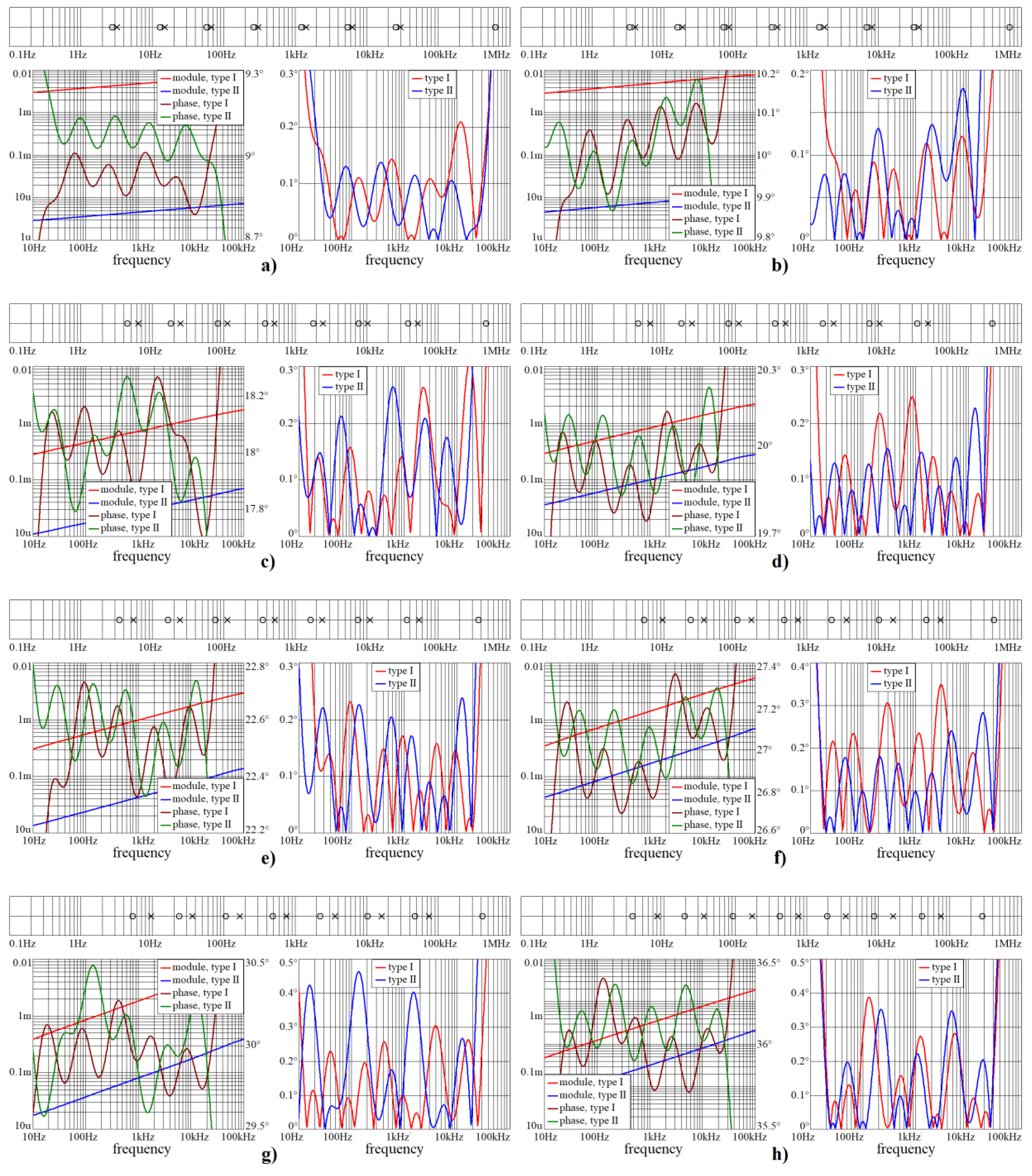
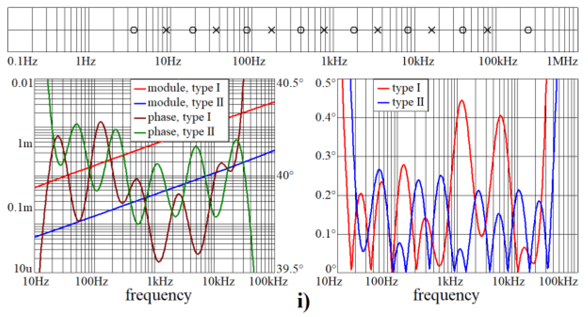
This subsection demonstrates the numerical verification of designed audio and wideband CPEs using Mathcad. Module and phase frequency responses (lower left plots), together with absolute error (lower right plots), are calculated in the frequency range starting with 10 Hz and ending with 100 kHz, which is suitable for audio CPEs. Within these pictures, the locations of zeroes and poles of the complex admittance function are also provided (upper plot). Individual results are provided in Figure 3 and Figure 4.
Provided visualizations clearly prove that individual calculated CPE approximations are in very good agreement with ideal CPE, i.e., promised accuracy were reached. Non-symmetrical phase ripples are caused by real-valued RC components inside analyzed CPE.

4. Applications of CPE

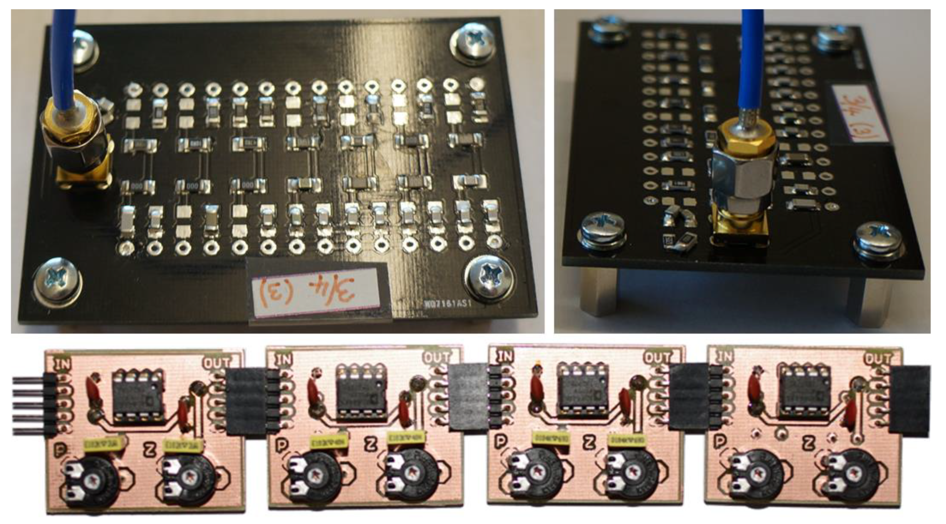
This section is aimed at giving the reader some ideas, i.e., practical examples, of analog systems that utilize one or several of the CPEs provided in Section 3 of this paper. Figure 5 demonstrates two fabricated printed circuit boards (PCBs) dedicated for realization of CPEs. The first is fully passive in the sense of Figure 1a, where each resistor and capacitor connected in a single branch is composed of a series/parallel combination of three resistors and three capacitors, respectively. Note that, if necessary, shunt components are employed to make a proper connection. Board organization and SMD components minimize the parasitic properties of the PCB and its negative effects on CPE approximation. This renders the PCB useful for frequencies up to tens of MHz. A second PCB shows active realization of CPEs based on two-ports, given in Figure 1i.
The upcoming demonstration examples require a very good approximation of CPEs. For audio phase shifters, accuracy is a key property, because a smooth transition between two points located on the phase frequency response of a designed two-port is our goal. A reduced Baxandal’s circuit, as well as subsonic oscillator, is an example of less demanding applications of the designed CPEs. However, heavily rippled CPEs can cause uncertainties in the specification of the oscillation frequency. Practical experience with applications of derived CPEs shows, once again, that all approximations are extremely sensitive to the numerical values of resistors and capacitors. Thus, the general recommendation is to make careful selections and measure real values of all passive components before assembling on the PCB.

4.1. Application of Audio CPEs in Non-Asymptotical Phase Shifters

Acoustic effects are a class of signal processing tasks which operates with continuous waveforms and frequency bands, beginning with 20 Hz and ending with 20 kHz. There are three sources of audio signals: human performance, instrumentation music, and computer-aided sound synthesis. After generation, all sources subjected to further processing that can be marked as basic, such as amplification, attenuation, mixing, or equalization. Advanced audio operations, such as the surround effects and 3D illusion design, require either black-boxed digital signal processing or a sequence of two-ports with predefined phase frequency responses. Fully analog realization of the arbitrary phase shifters proposed in this example can be easily adopted by readers and re-used in their specific situations, i.e., for different shapes of rooms or the location of audio sources, speakers, or the listener.
Basically, there are two types of integer-order analogue phase shifters. The first class perform asymptotical phase change, i.e., the phase approaches an initial and final value that is ±90° k, where k is the natural number, for DC and infinite frequency, respectively. Obviously, all types of frequency filters, including all-pass sections, are members of this extensive class of analog electronic systems. Standard filters can also be utilized for a non-asymptotical phase shifting. However, we cannot arbitrarily choose and connect two points on the phase frequency response by using a curve that is monotonically decreasing. On the other hand, the appropriate combination of integer-order and FO two-ports can treat all the problems mentioned. Missing operation, i.e., fully arbitrary phase shifting in a selected frequency range, becomes the topic of this first example. However, remember that phase shifting using an FO circuit causes the deformation of group delay and linear distortion.
A common strategy for the utilization of CPEs in a continuous-time filtering application is to replace the standard linear capacitor with CPEs. However, such a substitution changes the definition of a significant frequency and, in specific circumstances, the type of filter itself. For example, a bad identification of the filter type can be found in [68], where an FO all-pass filter is incorrectly reported. For a phase shifting purpose, we can directly adopt the transfer function of the first-order low-pass filter generalized into an FO domain. For the given starting point {f1, φ1} and final point {f2, φ2}, both located on a phase frequency response, the significant frequency ω0 and total circuit order α is the solution of the two nonlinear equations
φ k ( ω ) = a t a n [ ( 2 · π · f k ) α · s i n ( π · α 2 ) ω 0 + ( 2 · π · f k ) α · c o s ( π · α 2 ) ] ,
where k = 1, 2 is the index of a point on the phase frequency response. If a larger phase shift between the two selected frequency points is requested and final realization in the form of single two-port is required, than the transfer function of an integer-order all-pass filter can be generalized into an FO domain. In this case, simple replacement of the standard capacitor with CPEs does not produce a flat module frequency response, and can no longer be referred to as an all-pass filter. The FO pole angular frequency, ω0, and the mathematical order, α, is the solution to the following coupled equations
φ k ( ω ) = a t a n [ ( 2 · π · f k ) α · s i n ( π · α 2 ) ( 2 · π · f k ) α · c o s ( π · α 2 ) ω 0 ] a t a n [ ( 2 · π · f k ) α · s i n ( π · α 2 ) ( 2 · π · f k ) α · c o s ( π · α 2 )   +   ω 0 ] ,
where, again, k = 1, 2.
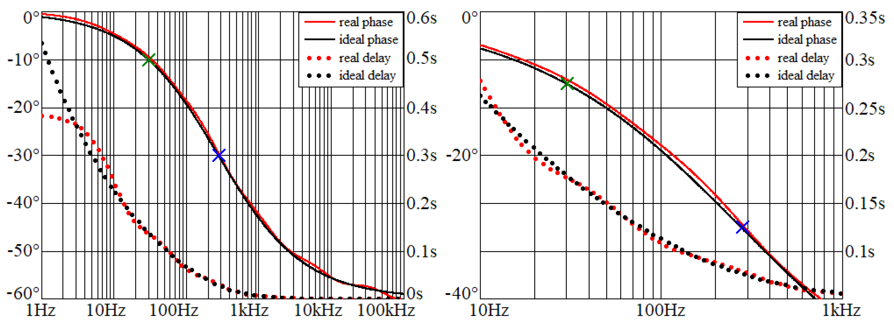
Example I: Suppose that a bass-band phase shift transformation {30 Hz, −10°}→{280 Hz, −30°} with an uncorrected group delay is requested. By solving System (16), we obtain the solution for significant frequency f0 = 23 Hz and order α = 2/3. Ideal and real voltage transfer functions in the Laplace transform (to be implemented as electronic circuit) can be expressed as
K i d e a l ( s ) = 2 π f 0 s 2 / 3 + 2 π f 0 K r e a l ( s ) = 1 / R Y ( s ) + 1 / R ,
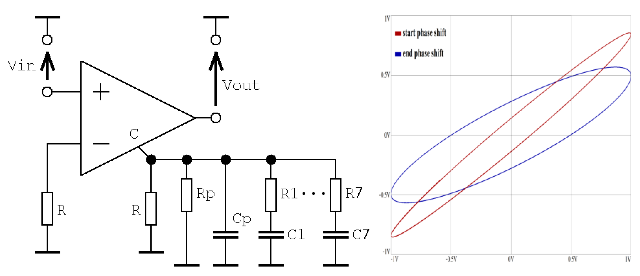
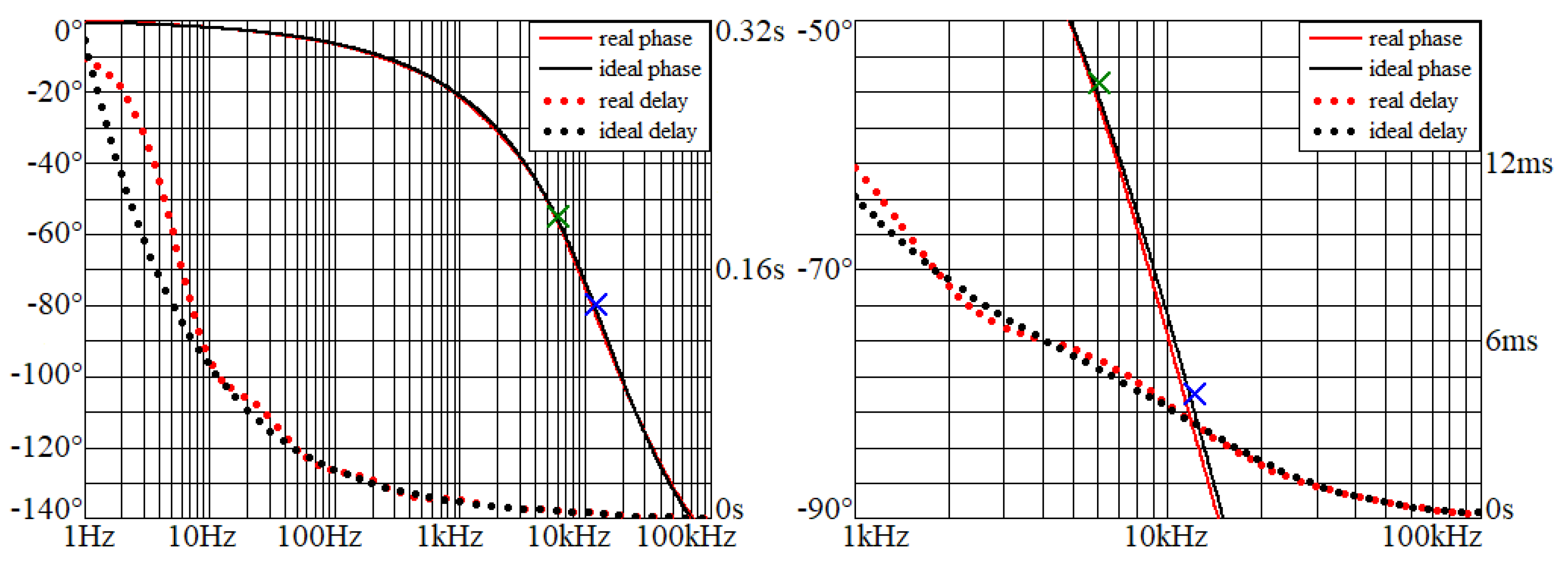
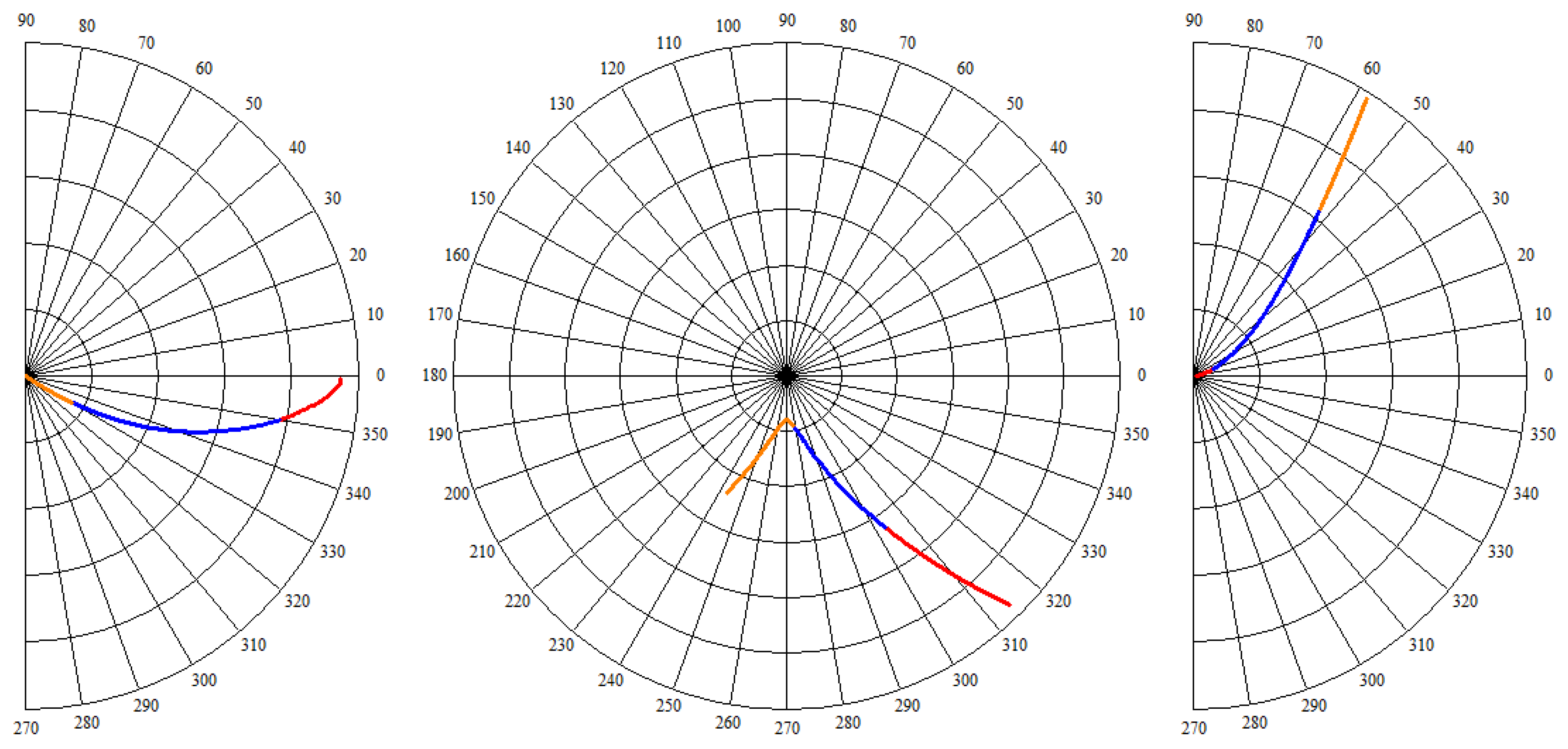
where Y(s) is the admittance function of CPE approximation (1), and the time constant of the phase shifter is formed by the pseudo-capacitance taken from Section 3.13 together with resistance R = 70 Ω. A graphical illustration of the obtained results (Orcad Pspice circuit simulation data imported to Mathcad, AC sweep analysis) is provided in Figure 6. Here, green and blue crosses represent the start and end points in the phase frequency response, respectively. One simple network realization with off-the-shelf active elements of this kind of phase shifter is demonstrated in Figure 7. Note that the major parasitic properties of AD844—namely input resistance of a low-impedance input inverting terminal, as well as output impedance of the current output C terminal—can be neglected, or, speaking more precisely, included into values of working resistances R. The infinite input impedance makes this two-port a good candidate for a cascade synthesis and can cooperate with other voltage-mode filters.
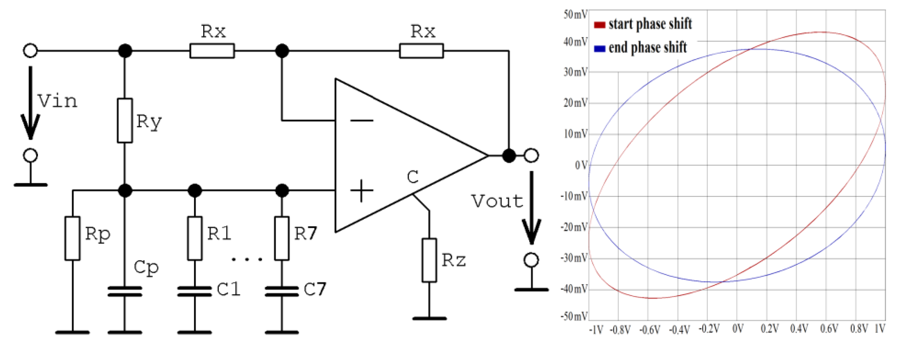
Example II: Assume a treble-band phase shift transformation represented by connection of two points {6 kHz, −55°}→{12150 Hz, −80°}. The solution of System (14) yields significant frequency f0 = 27 kHz and order α = 1.151. Simple replacement of a capacitor with standard CPEs (implemented using passive RC approximation) cannot be done, and some sort of immittance multiplier should be employed. However, by solving Formula (17) with the given input parameters yields an FO pole frequency f0 = 49 Hz and order α = 0.5. Thus, CPEs suitable for this application can be taken directly from Section 3.10. Corresponding simulation outputs are shown in Figure 8, while possible circuit realization is demonstrated in Figure 9, namely in the upper right schematic. The proposed two-port is derived from the common structure of operational-amplifier-based first-order voltage-mode all-pass filters. The ideal and real voltage transfer functions required by this application are
K i d e a l ( s ) = s 1 / 2 2 π f 0 s 1 / 2 + 2 π f 0 K r e a l ( s ) = Y ( s ) 1 / R Y ( s ) + 1 / R ,
where Y(s) is admittance function of CPE approximation (1). If pseudo-capacitance 85.25 μF/s1/2 is adopted, numerical values of resistors should be chosen as RX = 10 kΩ, RY = 36 Ω, and RZ = 1 kΩ.
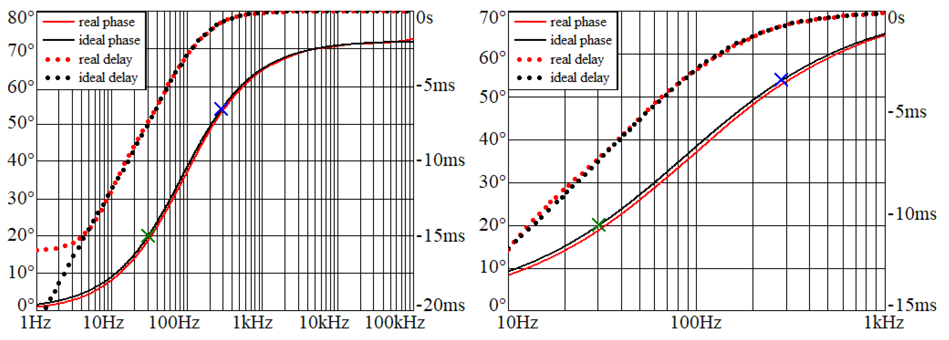
Example III: Assume that an increasing phase in the bass-band is demanded; namely the connection of points {30 Hz, 20°}→{280 Hz, 54°}. Then, a combination of the positive right-hand side of Equivalency (16) and Inverse Transfer Function (18), i.e.,
K i d e a l ( s ) = s 2 / 3 + 2 π f 0 2 π f 0 K r e a l ( s ) = 1 R i ( 1 / R o + 1 / R c ) · Y ( s ) · R i + 1 Y ( s ) · R + R / R i + 1 ~ Y ( s ) + 1 / R 1 / R ,
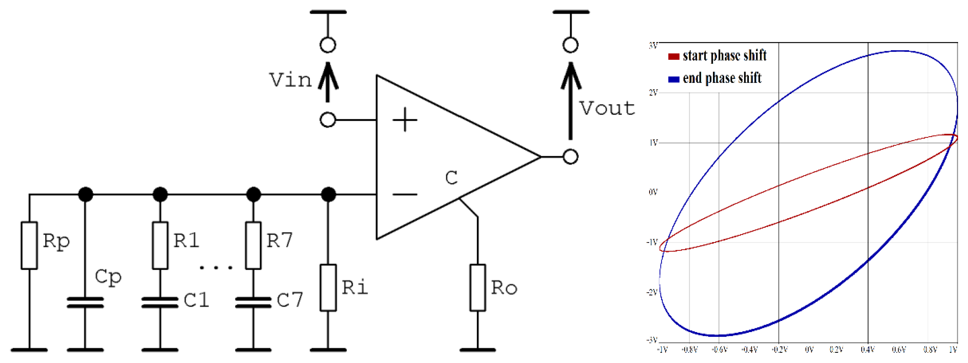
where input resistance of current input terminal was neglected. For the CPEs defined in Section 3.17 (phase shift 72°) and pseudo-capacitance 1.33 μF/s1/5, the value of both working resistors is Ri = Ro = 4.9 kΩ. The corresponding calculated results can be found in Figure 10, and a circuit capable to handle with this phase transform is depicted in Figure 11. In this case, as evident from Transfer Functions (20), the input resistance of the negative input terminal of AD844, denoted as R, as well as the output resistance of the current output RC cannot be simply neglected in our considerations. In practice, this problem causes 2° of intrinsic error that can, however, be compensated.
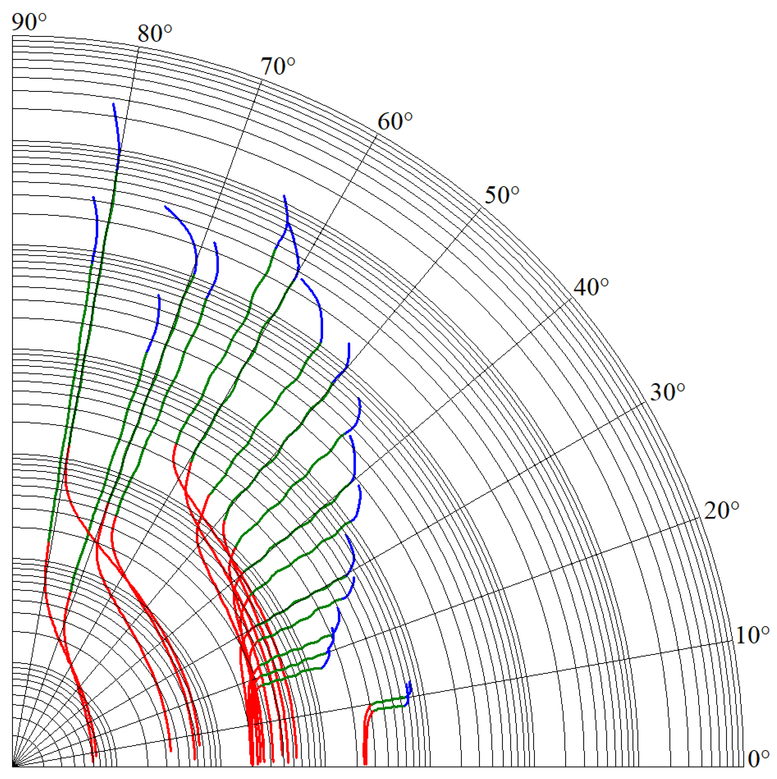
In addition to the integer-order asymptotical phase shifters, where the phase difference between the output and input circuit variable is k-times 90°, this brief example offers a circuit solution for a truly arbitrary phase shifter; however, at the cost of a deformed group delay and linear distortion. Polar plots of the complex transfer functions of all examples of phase shifters mentioned above are provided in Figure 12. The band-reject nature of Transfer Function (19) is evident.

4.2. Implementation of Audio CPEs in Bass-Band Corrector

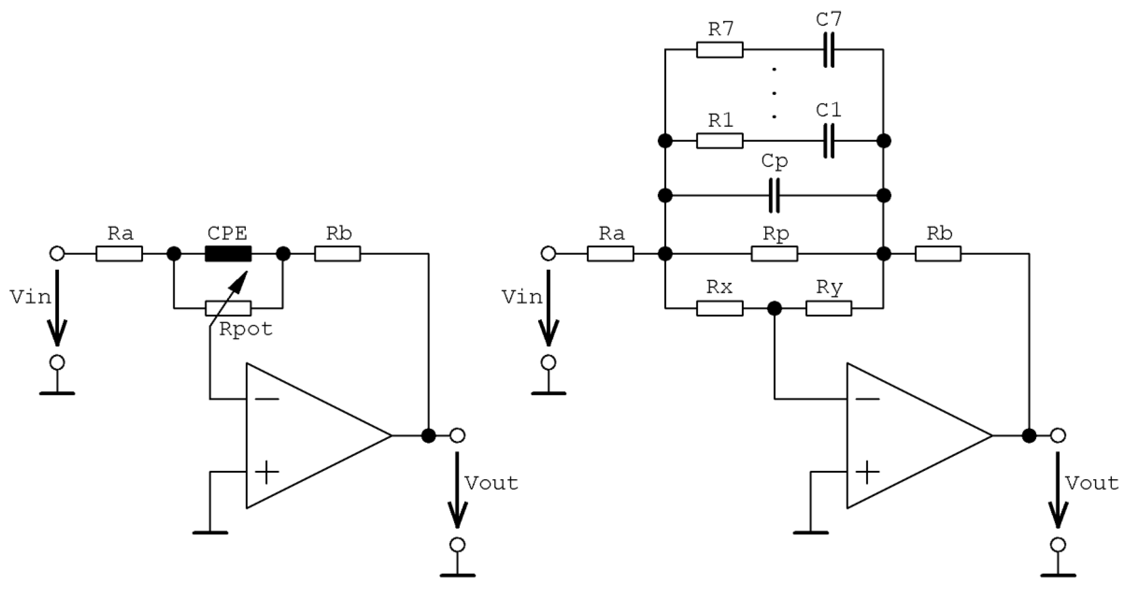
A proposed bass-band corrector can be considered as a half-circuit known as Baxandal’s corrector, a well-known building block that can be found in most discrete realizations of audio amplifiers. Its fundamental function is to independently strengthen or suppress the module frequency response in low bands (bass correction) and high bands (treble correction). The standard topology of Baxandal’s circuit utilizes a single active element—a voltage feedback operational amplifier. Using single CPEs designed in Section 3, the bass-corrector can be separated (see Figure 13). The module frequency response is affected by the actual position of the potentiometer slider; let us mark its location as k. For the left corner, where k = 0, and right corner, where k = 1, the voltage transfer functions are
K l e f t ( s ) = 1 R 1 · s α Y 0 R 2 R y + R 2 + R y s α Y 0 R y + 1 ~ R 1 R 2 · s α + 1 / ( Y 0 R 2 ) s α , K r i g h t ( s ) = R 2 s α Y 0 R x + 1 s α Y 0 R 1 R x + R 1 + R x ~ R 1 R 2 · s α s α + 1 / ( Y 0 R 1 ) ,
where Y0 is the pseudo-capacitance of a chosen CPE, α is the mathematical order of this CPE, and the value of potentiometer (Ry in the case of Kleft and Rx for Kright) is supposed to be much higher than the impedance of the CPE in the audio band and R1,2. To achieve the same roll-off frequency for bass strengthening and suppression, the condition R1 = R2 needs to be satified. For an ideal operational amplifier and general position of the potentiometer’s slider k ∈ (0, 1), the resulting voltage transfer function can be expressed as
K g e n e r a l ( s ) = s α Y 0 R 2 R p o t + R 2 + R p o t ( 1 k ) s α Y 0 R 1 R p o t + R 1 + R p o t · k = K 0 s α + ω Z s α + ω P ,
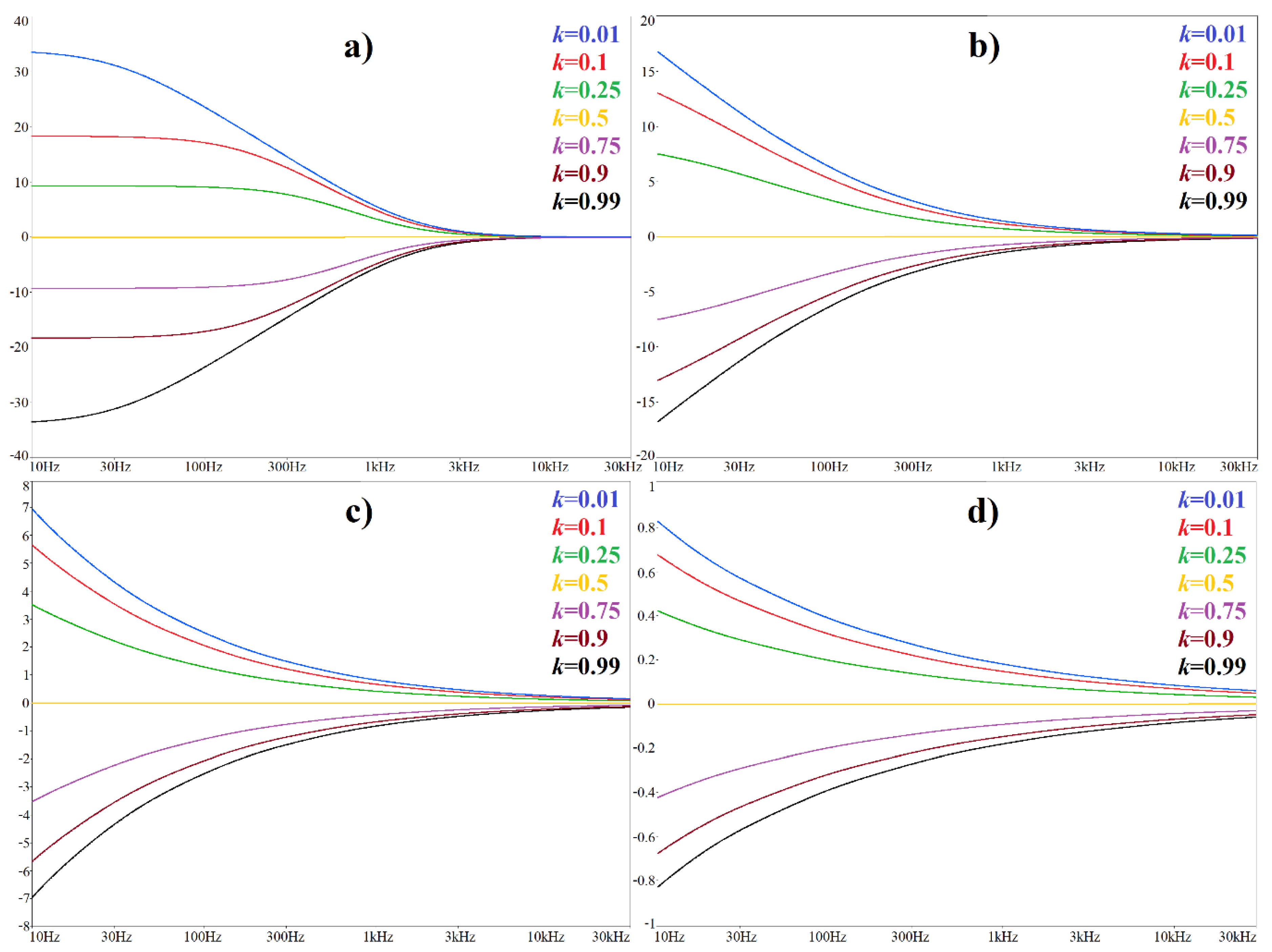
where Rpot represents the value of the potentiometer. Obviously, the slider position in the centre of trace k = 0.5 means that no correction is applied.
An Orcad Pspice circuit simulation (AC sweep analysis) of a standard and CPE-based bass-corrector (see Figure 13) is provided in Figure 14. For α = 1, the numerical values of circuit components are R1 = R2 = 1 kΩ and C = 100 nF, leading to significant frequency f0 = 1.6 kHz. For α = 2/3, the choice of resistances R1 = R2 = 100Ω and CPEs from Section 3.13 lead to f0 = 60 Hz. For order α = 1/2, the choice of resistances R1 = R2 = 1 kΩ and CPEs taken from Section 3.10 lead to f0 = 1.9 Hz. Finally, for α = 1/3, the choice of resistances R1 = R2 = 22 kΩ and CPEs from Section 3.7 lead to f0 = 0.07 Hz. CPEs allow for smooth continuous corrections over the entire audio frequency band. Of course, the order of CPEs is a part of this “acoustic effect”.

4.3. Application of Audio CPEs in Subsonic Two-Port Phase Keeper

This subsection describes design process toward an electronically tunable generator of harmonic waveforms. A two-port CPE is used to provide a constant angle difference between the two node voltages, over a frequency range dedicated to electronic tuning. The design flow can be divided into four steps. Firstly, for two-terminal passive CPEs picked from Section 3, the positions of zeroes and poles are calculated. Secondly, the approximation is transformed into the subsonic band via frequency rescaling. Next, the CPE is transformed into two-port as shown in Figure 1i. Finally, the CPE is inserted into a closed loop together with only one additional two-port— a first-order all-pass filter (APF) with amplification. This structure will work if Berkhausen’s conditions for oscillation are satisfied simultaneously.
Assume that a 20° phase shift between two node voltages needs to be kept over the frequency range 100 μHz to 1 Hz. Both passive ladder RC approximants of CPEs provided in Section 3.4 can be transformed into the desired frequency range by introducing the new frequency norm γ = 10−5. This operation moves whole phase frequency responses horizontally into the desired band. To do this, values of all the capacitors need to be divided by γ while the resistors remain unchanged. Obviously, these significantly increased values capacitors can cause the CPEs to no longer be implementable by commercially available components. This problem can be still avoided by the application of impedance rescaling ψ. This is real number that moves the module frequency response vertically without changing the phase frequency response. It can be applied by dividing the values of all capacitors by ψ while the values of all resistors are increased ψ times. For example, the application of ψ = 100 and γ = 10−5 on the passive components given in Table 8 leads to set Rp = 500 kΩ, R1 = 1.25 MΩ, R2 = 890 kΩ, R3 = 640 kΩ, R4 = 460 kΩ, R5 = 320 kΩ, R6 = 240 kΩ, R7 = 160 kΩ, Cp = 900 nF, C1 = 2 mF, C2 = 732 μF, C3 = 224 μF, C4 = 69 μF, C5 = 21 μF, C6 = 6.4 μF, and C7 = 2 μF. These values can still be implemented using a combination of existing discrete passive components. However, different realizations of subsonic oscillator will be suggested.
Let us adopt the values of resistors and capacitors provided in Table 8. By substitution of these values into Equation (1), and by algebraic manipulations with resulting fraction, we obtain following coefficients of the numerator of (5)
a 8 = 3.28 · 10 12 , a 7 = 9.04 · 10 18 , a 6 = 2.33 · 10 24 , a 5 = 1.14 · 10 29 , a 4 = 1.2 · 10 33 , a 3 = 2.73 · 10 36 ,   a 2 = 1.36 · 10 39 , a 1 = 1.45 · 10 41 ,   a 0 = 2.98 · 10 42 ,
together with the denominator of (5)
b 7 = 3.65 · 10 21 ,   b 6 = 1.45 · 10 26 ,   b 5 = 1.01 · 10 28 ,   b 4 = 1.49 · 10 36 , b 3 = 4.74 · 10 39 , b 2 = 3.3 · 10 42 ,   b 1 = 5 · 10 44 , b 0 = 1.49 · 10 46 .
Having admittance function as a fraction in a semi-symbolic form, we can easily calculate the roots of both polynomials. Hence, we obtain the locations of zeroes and poles that occur in Formula (6), namely
ω Z 1 = 27 rad s ,   ω Z 2 = 110 rad s ,   ω Z 3 = 499 rad s , ω Z 4 = 2.26 krad s , ω Z 5 = 10.54 krad s ,   ω Z 6 = 47.08 krad s , ω Z 7 = 220.5 krad s ,   ω Z 8 = 2.47 Mrad s ,
and
ω P 1 = 40 rad s ,   ω P 2 = 154 rad s , ω P 3 = 698 rad s , ω P 4 = 3.15 krad s , ω P 5 = 14.9 krad s , ω P 6 = 65 krad s ,   ω P 7 = 312.5 krad s .
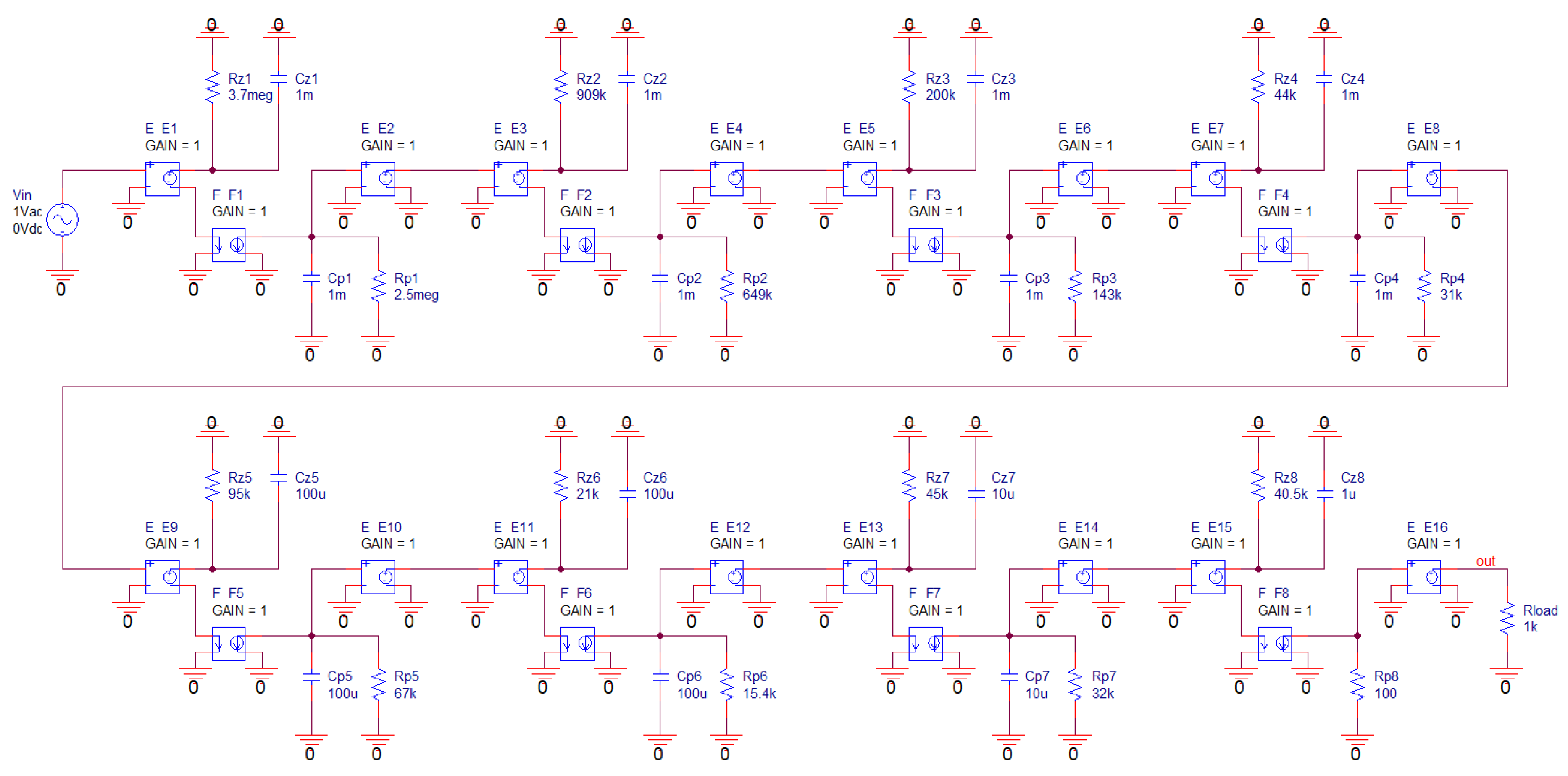
Now, to move CPE approximation to a subsonic frequency band, each angular frequency should be multiplied by a norm γ = 10−5. As already mentioned, the CPE will be designed as two-port by a cascade connection of general bilinear filters as depicted in Figure 15. Thus, numerical values of resistors and capacitors can be obtained as
2.7 · 10 4 = 1 R Z 1 C Z 1 ,   1.1 · 10 3 = 1 R Z 2 C Z 2 , 5 · 10 3 = 1 R Z 3 C Z 3 , 0.023 = 1 R Z 4 C Z 4 ,   0.105 = 1 R Z 5 C Z 5 , 0.471 = 1 R Z 6 C Z 6 ,   2.2 = 1 R Z 7 C Z 7 , 24.7 = 1 R Z 8 C Z 8 ,   4 · 10 4 = 1 R P 1 C P 1 ,   1.54 · 10 3 = 1 R P 2 C P 2 , 0.007 = 1 R P 3 C P 3 ,   0.032 = 1 R P 4 C P 4 , 0.149 = 1 R P 5 C P 5 ,   0.651 = 1 R P 6 C P 6 ,   3.125 = 1 R P 7 C P 7 .
Orcad Pspice verification of this CPE in frequency and time domain is demonstrated in Figure 16. The simulation profile was set as final time 104 s and time step 100 ms.
Of course, values (23) and (24) can be obtained if the capacitors taken from Table 8 are divided by the frequency norm γ then substituted into (1) through algebraic manipulations, or using Mathcad’s collect item from the Symbolic toolbox, transformed into semi-symbolic Fraction (5), and polynomials of this fraction are used for root calculations (in Mathcad, the keyword polyroots can be used).
Both mentioned approaches can also be applied on the second parallel-series structure of RC two-terminal CPEs.

5. Discussion

The orientation of this paper is two-sided. Firstly, it provides deep investigation of research papers focused on the design and applications of CPEs in analog electrical engineering. This section reveals the current progress in this emerging scientific field such that an interested reader can find their own path to future research topics and answer the as-yet unsolved problems.
CPEs have significant potential in audio applications, for example, to generate specific sound effects, create audio filters or user-defined audio correctors, equalizers, etc. Because of these reasons, passive ladder-type realizations of CPEs dedicated to the frequency range beginning with 20 Hz and ending at 20 kHz for 19 different mathematical orders have been proposed. Each approximation utilizes resistors and capacitors taken from the fabrication series E12 and arranged in basic series and/or parallel combinations to concretize real experimental implementations of CPE two-terminal devices.
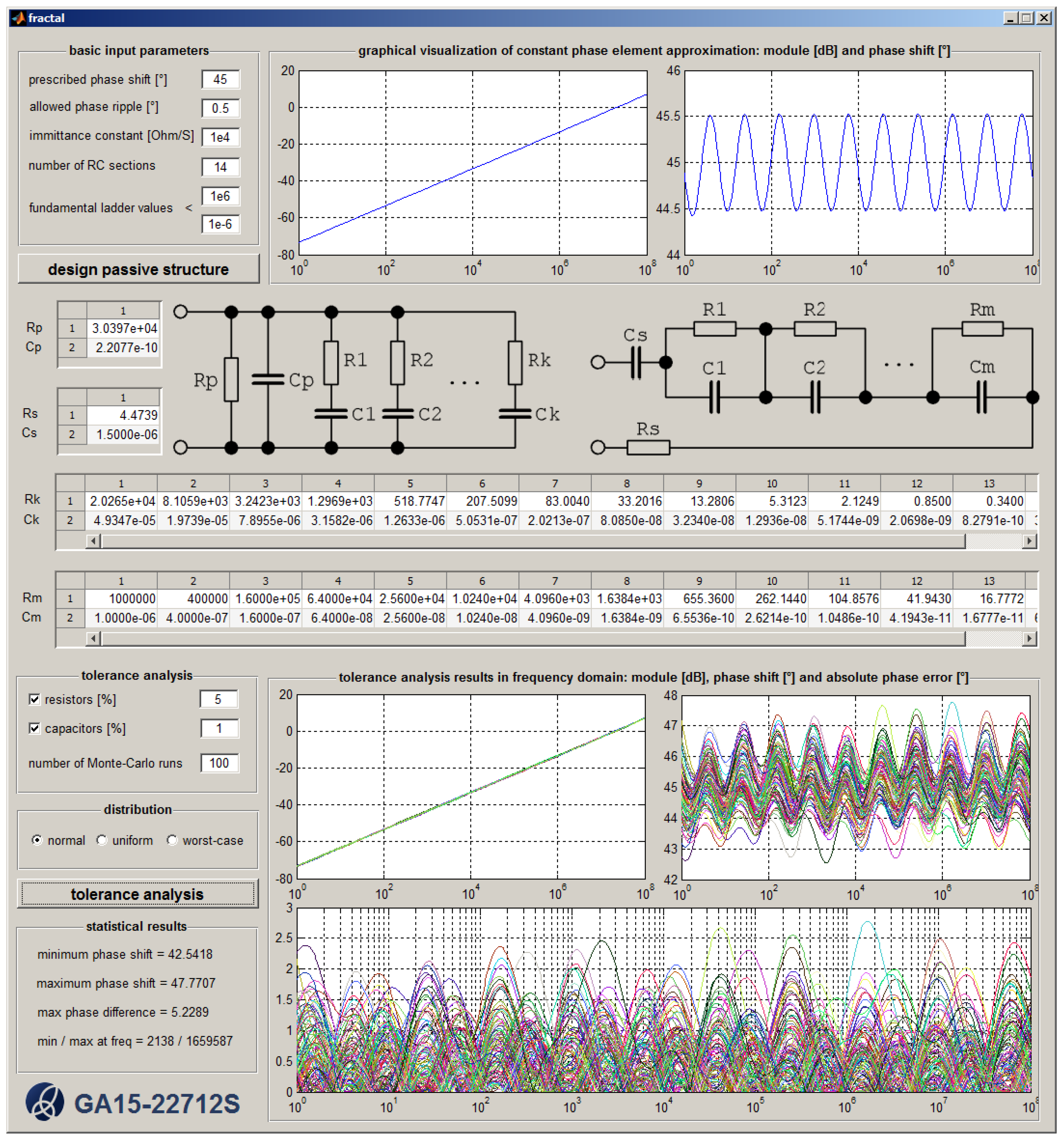
A short program in Matlab for easy design of passive CPE approximants has been created; check Figure 17 for a visualization of a certain example. The calculation engine is a direct implementation of algorithms proposed by Professor Valsa and is summarized in [15,16]. Software is able to analyze designed passive CPEs from the viewpoint of fabrication tolerances. If a curious reader is interested in either problems connected with CPE synthesis or the mentioned piece of software, please do not hesitate to contact the author (preferably via email). A free copy of this Matlab software can be delivered. The software works well with Matlab version 2013 and higher, together with a monitor/display resolution of 1920 × 1080 and higher.
Some authors run stochastic optimization methods to reach the best numerical values of the components of passive or active CPEs. For example, a genetic algorithm was used in [69]. However, in this case, an optimal design is given by the exact formulas and the application of additional mathematical tools, especially techniques dedicated to global optimization, is questionable. On the other hand, a slight adjustment of the first and last zero-pole location can create phase overshoot and improve or enlarge the frequency band for the application of CPEs.
Section 4 suggests a new two-port circuit element that can perform arbitrary phase shifting, i.e., a non-asymptotical phase change that can connect any two points on a phase frequency response. This can be understood as generalization of asymptotical phase shifting. For a phase change from DC to infinity that begins with a value other than 90·n° (n being integer number), only an FO integrator or FO differentiator should be placed before an FO phase shifter [49,50] (if the phase starts in the first of fourth segment of the polar plane of a complex transfer function) together with an inverting amplifier (to begin the phase shifting process in the second or third segment of the polar plane of a complex transfer function).
Remember that CPEs suggested in Section 3 of this paper are designed with pre-defined values of impedance norm ξ. This factor can be adjusted (change of the pseudo-capacitance), and this process is equivalent to a shift in module frequency response vertically upward (ξ > 1) or downward (ξ < 1) while the phase frequency response remains unchanged. To make renormalization, each capacitor needs to be divided by ξ while each resistor is multiplied by the same amount ξ. Approximation of CPEs using a fully passive ladder circuit is also not restricted to a fixed frequency band. For example, each designed CPE dedicated to audio signal processing can be transformed into a subsonic or ultrasonic frequency band by introducing frequency scaling factors γ < 1 and γ > 1, respectively. This scaling factor is a real positive number that reduces the value of the k-th capacitor to Ck/γ, and decreases the value of the k-th inductor to Lk/γ. The values of the resistors remain unchanged. Of course, transformed CPEs are implementable if values of accumulation elements are still reasonable, off-the-shelf components.
Each designed CPE undergoes Monte Carlo analysis, namely 1000 runs of AC sweep in Orcad Pspice for a normal distribution of the random values of the passive components. It turns out that the high-precision passive components need to be considered for CPE design. Larger fabrication tolerances (0.5%, 1%, etc.) cause too large phase errors. This means that the phase frequency response is heavily rippled, and neighborhood peaks of the phase pantile can add up, leading to the maximal phase deviation being significantly raised. Based on personal experiences of author, a maximal phase error greater than 3° over the approximated frequency range renders designed CPEs useless, because individual orders become undistinguishable. Of course, the usability of designed CPEs depends on the concrete application.

6. Conclusions

This paper brings forth a wide range of high-precision CPEs dedicated to audio signal processing. The networks presented here are two-terminals; required alternation of poles and zeroes of immittance function is obtained by the interconnection of linear resistors and capacitors. Readers can pick and use drafted CPEs directly without need for additional calculations. Each designed CPE has reasonable values of circuit components that can be found commonly in shops. Furthermore, two different passive network alternatives are provided for CPEs. Although several very recent manufacturing techniques lead to “good” CPEs [70], CPE approximation circuits still have a long future.
Two-ports proposed in the individual examples can find interesting applications in fully analog acoustic and subsonic signal processing. In fact, any three-decades-wide frequency band can be reached via frequency rescaling. CPEs are extremely phase-accurate, but the final precision is also a matter of manual dexterity. This paper provides material for wide spectrum of enthusiasts, electronic engineers, and design specialist focused on the construction of FO circuits.
It has been also mentioned that there are some research papers that provide questionable results coming from the utilization of imperfect CPEs. In such cases, existing structures of FO filters, harmonic oscillators, arbitrary waveform generators, phase correctors, PID controllers, regulators, models of dynamical systems, etc. can be simulated again, and associated results can be polished.

Funding

Research described in this paper was financed by the National Sustainability Program under Grant LO1401. For the research, infrastructure of the SIX Center was used.

Conflicts of Interest

The author declares no conflict of interest.

References

  1. Ortigueira, M.D. An introduction to the fractional continuous-time linear systems. IEEE Circuits Syst. Mag. 2008, 8, 19–26. [Google Scholar] [CrossRef]
  2. Elwakil, A.S. Fractional-order circuits and systems: An emerging interdisciplinary research area. IEEE Circuits Syst. Mag. 2010, 10, 40–50. [Google Scholar] [CrossRef]
  3. Hirschorn, B.; Orazem, M.E.; Tribollet, B.; Vivier, V.; Frateur, I.; Musiani, M. Constant-phase-element behavior caused by resistivity distributions in films. J. Electrochem. Soc. 2010, 157, 452–457. [Google Scholar] [CrossRef]
  4. Bisquert, J.; Garcia-Belmonte, G.; Bueno, P.; Longo, E.; Bulhoes, L.O.S. Impedance of constant phase element (CPE)-blocked diffusion in film electrodes. J. Electroanal. Chem. 1998, 452, 229–234. [Google Scholar] [CrossRef]
  5. Zoltowski, P. On the electrical capacitance of interfaces exhibiting constant phase element behavior. J. Electroanal. Chem. 1998, 443, 149–154. [Google Scholar] [CrossRef]
  6. Kochowski, S.; Nitsch, K. Description of the frequency behavior of metal-SiO2-GaAs structure characteristics by electrical equivalent circuit with constant phase element. Thin Solid Films 2002, 415, 133–137. [Google Scholar] [CrossRef]
  7. Biswas, K.; Sen, S.; Dutta, P.K. Realization of a constant phase element and its performance study in a differentiator circuit. IEEE Trans. Circuits Syst. II Express Briefs 2006, 53, 802–806. [Google Scholar] [CrossRef]
  8. Shoar Abouzari, M.R.; Berkemeier, F.; Schmitz, G.; Wilmer, D. On the physical interpretation of constant phase elements. Solid State Ion. 2009, 180, 922–927. [Google Scholar] [CrossRef]
  9. Agambayev, A.; Patole, S.; Farhat, M.; Elwakil, A.; Bagci, H.; Salama, K.N. Ferroelectric fractional-order capacitors. ChemElectroChem 2017, 4, 2807–2813. [Google Scholar] [CrossRef]
  10. Carlson, G.; Halijak, C. Approximation of fractional capacitors (1/s)^(1/n) by a regular newton process. IEEE Trans. Circuit Theory 1964, 11, 210–213. [Google Scholar] [CrossRef]
  11. Halijak, C. An RC impedance approximant to (1/s)^{1/2}. IEEE Trans. Circuit Theory 1964, 11, 494–495. [Google Scholar] [CrossRef]
  12. Steiglitz, K. An RC impedance approximant to s^{-1/2}. IEEE Trans. Circuit Theory 1964, 11, 160–161. [Google Scholar] [CrossRef]
  13. Radwan, A.G.; Salama, K.N. Fractional-order RC and RL circuits. Circuits Syst. Signal Process. 2012, 31, 1901–1915. [Google Scholar] [CrossRef]
  14. Dutta Roy, S.C.; Shenoi, B.A. Distributed and lumped RC realization of a constant argument impedance. J. Frankl. Inst. 1966, 282, 318–329. [Google Scholar] [CrossRef]
  15. Valsa, J.; Vlach, J. RC models of a constant phase elements. Int. J. Circuit Theory Appl. 2013, 20, 59–67. [Google Scholar] [CrossRef]
  16. Valsa, J.; Dvorak, P.; Friedl, M. Network model of the CPE. Radioengineering 2011, 20, 619–626. [Google Scholar]
  17. Vinagre, B.M.; Podlubny, I.; Feliu, V. Some approximations of fractional order operators used in control theory and applications. J. Fract. Calc. Appl. Anal. 2000, 3, 231–248. [Google Scholar]
  18. Sotner, R.; Jerabek, J.; Petrzela, J.; Domansky, O.; Tsirimokou, G.; Psychalinos, C. Synthesis and design of constant phase elements based on the multiplication of electronically controllable bilinear immittances in practice. AEU Int. J. Electron. Commun. 2017, 78, 98–113. [Google Scholar] [CrossRef]
  19. Sotner, R.; Jerabek, J.; Petrzela, J.; Dostal, T. Simple approach for synthesis of fractional-order grounded immittances based on OTAs. In Proceedings of the 39th International Conference on Telecommunications and Signal Processing, Vienna, Austria, 27 June 2016; pp. 563–568. [Google Scholar] [CrossRef]
  20. Petrzela, J. Fundamental analog cells for fractional-order two-port synthesis. In Proceedings of the 23rd International Conference Radioelektronika, Pardubice, Czech Republic, 16 April 2013; pp. 182–187. [Google Scholar] [CrossRef]
  21. Petrzela, J.; Sotner, R.; Guzan, M. Implementation of constant phase elements using low-Q band-pass and band-reject filtering sections. In Proceedings of the 21th International Conference on Applied Electronics, Pilsen, Czech Republic, 6 September 2016; pp. 205–209. [Google Scholar] [CrossRef]
  22. Tsirimokou, G.; Kartci, A.; Koton, J.; Herencsar, N.; Psychalinos, C. Comparative study of discrete component realizations of fractional-order capacitor and inductor active emulators. J. Circuits Syst. Comput. 2018, 27, 1850170. [Google Scholar] [CrossRef]
  23. Tsirimokou, G.; Kartci, A.; Koton, J.; Herencsar, N.; Psychalinos, C. Comparative study of fractional-order differentiators and integrators. In Proceedings of the 40th International Conference on Telecommunications and Signal Processing, Barcelona, Spain, 5 July 2017; pp. 714–717. [Google Scholar] [CrossRef]
  24. Petrzela, J. Design of complex fractional-order immittances for simple PID regulation. In Proceedings of the 40th International Conference on Telecommunications and Signal Processing, Barcelona, Spain, 5 July 2017; pp. 283–288. [Google Scholar] [CrossRef]
  25. Domansky, O.; Sotner, R.; Langhammer, L. Reconfigurable impedance converter for synthesis of integer and fractional-order synthetic elements. In Proceedings of the 41st International Conference on Telecommunications and Signal Processing, Athens, Greece, 4 July 2018; pp. 367–371. [Google Scholar] [CrossRef]
  26. Kartci, A.; Brancik, L. CFOA-based fractional-order oscillator design and analysis with NILT method. In Proceedings of the 27th International Conference Radioelektronika, Brno, Czech Republic, 19 April 2017; pp. 219–222. [Google Scholar] [CrossRef]
  27. Said, L.O.; Radwan, A.G.; Madian, A.H.; Soliman, A.M. Fractional order oscillators based on operational transresistance amplifiers. AEU-Int. J. Electron. C. 2015, 69, 988–1003. [Google Scholar] [CrossRef]
  28. Kartci, A.; Herencsar, N.; Koton, J.; Psychalinos, C. Compact MOS-RC voltage-mode fractional-order oscillator design. In Proceedings of the 23th European Conference on Circuit Theory and Design, Catania, Italy, 4 September 2017; pp. 1–4. [Google Scholar] [CrossRef]
  29. Radwan, A.G.; Soliman, A.M.; Elwakil, A.S.; Sedeek, A. On the stability of linear systems with fractional-order elements. Chaos Solitons Fractals 2009, 40, 2317–2328. [Google Scholar] [CrossRef]
  30. Radwan, A.G.; Elwakil, A.S.; Soliman, A.M. Fractional-order sinusoidal oscillators: Design procedure and practical examples. IEEE Trans. Circuits Syst. I Regul. Pap. 2008, 55, 2051–2063. [Google Scholar] [CrossRef]
  31. Maundy, B.; Elwakil, A.S.; Gift, S. On a multivibrator that employs a fractional capacitor. Analog Integr. Circuits Signal Process. 2010, 62, 99–103. [Google Scholar] [CrossRef]
  32. Radwan, A.G.; Soliman, A.M.; Elwakil, A.S. First-order filters generalized to the fractional domain. J. Circuits Syst. Comput. 2008, 17, 55–66. [Google Scholar] [CrossRef]
  33. Radwan, A.G.; Elwakil, A.S.; Soliman, A.M. On the generalization of second-order filters to the fractional-order domain. J. Circuits Syst. Comput. 2009, 18, 361–386. [Google Scholar] [CrossRef]
  34. Dvorak, J.; Langhammer, T.; Jerabek, J.; Koton, J.; Sotner, R.; Polak, J. Synthesis and analysis of electronically adjustable fractional-order low-pass filter. J. Circuits Syst. Comput. 2018, 27, 1850032. [Google Scholar] [CrossRef]
  35. Dvorak, J.; Langhammer, L.; Jerabek, J.; Koton, J.; Sotner, R.; Polak, J. Electronically tunable fractional-order low-pass filter with current followers. In Proceedings of the 39th International Conference on Telecommunications and Signal Processing, Vienna, Austria, 27 June 2016; pp. 587–592. [Google Scholar] [CrossRef]
  36. Jerabek, J.; Sotner, R.; Kubanek, D.; Dvorak, J.; Langhammer, L.; Herencsar, N.; Vrba, K. Fractional-order low-pass filter with electronically adjustable parameters. In Proceedings of the 39th International Conference on Telecommunications and Signal Processing, Vienna, Austria, 27 June 2016; pp. 569–574. [Google Scholar] [CrossRef]
  37. Jerabek, J.; Sotner, R.; Dvorak, J.; Langhammer, L.; Koton, J. Fractional-order high-pass filter with electronically adjustable parameters. In Proceedings of the 21st International Conference on Applied Electronics, Pilsen, Czech Republic, 6 September 2016; pp. 111–116. [Google Scholar] [CrossRef] [Green Version]
  38. Jerabek, J.; Sotner, R.; Dvorak, J.; Polak, J.; Kubanek, D.; Herencsar, N.; Koton, J. Reconfigurable fractional order filter with electronically controllable slope of attenuation, pole frequency and type of approximation. J. Circuits Syst. Comput. 2017, 26, 1750157. [Google Scholar] [CrossRef] [Green Version]
  39. Kubanek, D.; Koton, J.; Jerabek, J.; Ushakov, P.; Shadrin, A. Design and properties of fractional-order multifunction filter with DVCCs. In Proceedings of the 40st International Conference on Telecommunications and Signal Processing, Vienna, Austria, 27 June 2016; pp. 620–624. [Google Scholar] [CrossRef]
  40. Langhammer, L.; Sotner, R.; Dvorak, J.; Jerabek, J.; Polak, J. Fully-differential tunable fractional-order filter with current followers and current amplifiers. In Proceedings of the 27th International Conference Radioelektronika, Brno, Czech Republic, 19 April 2017; pp. 102–107. [Google Scholar] [CrossRef]
  41. Sotner, R.; Herencsar, N.; Jerabek, J.; Petrzela, J.; Dostal, T. Design of integer/fractional-order filter with electronically reconfigurable transfer responses. In Proceedings of the 24th IEEE International Conference on Electronics, Circuits and Systems, Batumi, Georgia, 5 December 2017; pp. 156–159. [Google Scholar] [CrossRef]
  42. Freeborn, T.J. Comparison of (1 + α) fractional-order transfer functions to approximate low-pass butterworth magnitude responses. Circuits Syst. Signal. Process. 2015, 35, 1983–2002. [Google Scholar] [CrossRef]
  43. Langhammer, L.; Sotner, R.; Dvorak, J.; Domansky, O.; Jerabek, J.; Uher, J. A 1 + α low-pass fractional-order frequency filter with adjustable parameters. In Proceedings of the 40st International Conference on Telecommunications and Signal Processing, Barcelona, Spain, 5 July 2017; pp. 724–729. [Google Scholar] [CrossRef]
  44. Kubanek, D.; Freeborn, T.J. (1 + α) fractional-order transfer functions to approximate low-pass magnitude responses with arbitrary quality factor. AEU Int. J. Electron. Commun. 2018, 83, 570–578. [Google Scholar] [CrossRef]
  45. Maundy, B.; Elwakil, A.S.; Freeborn, T.J. On the practical realization of higher-order filters with fractional stepping. Signal Process. 2011, 91, 484–491. [Google Scholar] [CrossRef]
  46. Freeborn, T.J.; Maundy, B.; Elwakil, A.S. Field programmable analogue array implementation of fractional step filters. IET Circuits Devices Syst. 2010, 4, 514–524. [Google Scholar] [CrossRef]
  47. Tsirimokou, G.; Sotner, R.; Jerabek, J.; Koton, J.; Psychalinos, C. Programmable analog array of fractional-order filters with CFOAs. In Proceedings of the 40th International Conference on Telecommunications and Signal Processing, Barcelona, Spain, 5 July 2017; pp. 706–709. [Google Scholar] [CrossRef]
  48. Herencsar, N.; Sotner, R.; Kartci, A.; Vrba, K. A novel pseudo-differential integer/fractional-order voltage-mode all-pass filter. In Proceedings of the IEEE International Symposium on Circuits and Systems, Florence, Italy, 27 May 2018; pp. 1–5. [Google Scholar] [CrossRef]
  49. Petrzela, J. Arbitrary phase shifters with increasing phase. In Proceedings of the 38th International Conference on Telecommunications and Signal Processing, Prague, Czech Republic, 9 July 2015; pp. 319–324. [Google Scholar] [CrossRef]
  50. Petrzela, J. Arbitrary phase shifters with decreasing phase. In Proceedings of the 37th International Conference on Telecommunications and Signal Processing, Berlin, Germany, 9 July 2014; pp. 682–686. [Google Scholar] [CrossRef]
  51. Lanusse, P.; Sabatier, J.; Oustaloup, A. Extension of PID to fractional orders controllers: A frequency-domain tutorial presentation. IFAC Proc. Vol. 2014, 47, 7436–7442. [Google Scholar] [CrossRef] [Green Version]
  52. Podlubny, I. Fractional-order systems and PIλDμ controllers. IEEE Trans. Autom. Control 1999, 44, 208–214. [Google Scholar] [CrossRef]
  53. Petras, I. The fractional-order controllers: Methods for their synthesis and application. J. Electr. Eng. 1999, 50, 284–288. [Google Scholar]
  54. Podlubny, I.; Petras, I.; Vinagre, B.M.; O′Leary, P.; Dorcak, L. Analogue realizations of fractional-order controllers. Nonlinear Dyn. 2002, 29, 281–296. [Google Scholar] [CrossRef]
  55. Ozbay, H.; Bonnet, C.; Fioravanti, A.R. PID controller design for fractional-order systems with time delays. Syst. Control Lett. 2012, 61, 18–23. [Google Scholar] [CrossRef] [Green Version]
  56. Petras, I. Fractional-order feedback control of a dc motor. J. Electr. Eng. 2009, 60, 117–128. [Google Scholar]
  57. Kadlcik, L.; Horsky, P. A low-dropout voltage regulator with a fractional-order control. Radioengineering 2016, 25, 312–320. [Google Scholar] [CrossRef]
  58. Chen, X.; Chen, Y.; Zhang, B.; Qui, D. A modeling and analysis method for fractional-order dc-dc converters. IEEE Trans. Power Electron. 2017, 32, 7034–7044. [Google Scholar] [CrossRef]
  59. Radwan, A.G.; Emira, A.A.; Abdelaty, A.M.; Azar, A.T. Modeling and analysis method of fractional-order dc-dc converter. ISA Trans. 2018, 82, 184–199. [Google Scholar] [CrossRef]
  60. Shu, X.; Zhang, B. The effect of fractional orders on the transmission power and efficiency of fractional-order wireless power transmission system. Energies 2018, 11, 1774. [Google Scholar] [CrossRef] [Green Version]
  61. Kathikeyan, R.; Akif, A.; Jafari, S.; Anitha, K.; Ismail, K. Chaotic chameleon: Dynamic analysis, circuit implementation, FPGA design and fractional-order form with basic analysis. Chaos Solitons Fractals 2017, 103, 476–487. [Google Scholar] [CrossRef]
  62. Munoz-Pacheco, J.M.; Zambrano-Serrano, E.; Volos, C.; Jafari, S.; Kengne, J.; Rajagopal, K. A new fractional-order chaotic system with different families of hidden and self-excited attractors. Entropy 2018, 20, 564. [Google Scholar] [CrossRef] [Green Version]
  63. Rajagopal, K.; Li, C.H.; Nazarimehr, F.; Karthikeyan, A.; Duraisamy, P.; Jafari, S. Chaotic dynamics of modified wien bridge oscillator with fractional order memristor. Radioengineering 2019, 28, 165–174. [Google Scholar] [CrossRef]
  64. Langhammer, T.; Dvorak, J.; Jerabek, J.; Koton, J.; Sotner, R. Fractional-order low-pass filter with electronic tunability of its order and pole frequency. J. Electr. Eng. 2018, 69, 3–13. [Google Scholar] [CrossRef] [Green Version]
  65. Sacu, I.E.; Alci, M. A current mode design of fractional-order universal filter. Adv. Electr. Comput. Eng. 2019, 19, 71–78. [Google Scholar] [CrossRef]
  66. Tsirimokou, G.; Koumousi, S.; Psychalinos, C. Design of fractional-order filters using current feedback operational amplifiers. J. Eng. Sci. Technol. Rev. 2016, 9, 77–81. [Google Scholar] [CrossRef]
  67. Kartci, A.; Herencsar, N.; Koton, J.; Brancik, L.; Vrba, K.; Tsirimokou, G.; Psychalinos, C. Fractional-order oscillator design using unity-gain voltage buffers and OTAs. In Proceedings of the 60th IEEE Midwest Symposium on Circuits and Systems, Boston, MA, USA, 6 August 2017; pp. 555–558. [Google Scholar] [CrossRef] [Green Version]
  68. Verma, R.; Pandey, N.; Pandey, R. Electronically tunable fractional order all pass filter. IOP Conf. Ser. Mater. Sci. Eng. 2017, 225, 012229. [Google Scholar] [CrossRef]
  69. Kartci, A.; Agambayev, A.; Farhat, M.; Herencsar, N.; Brancik, L.; Bagci, H.; Salama, K.N. Synthesis and optimization of fractional-order elements using a genetic algorithm. IEEE Access 2019, 7, 80233–80246. [Google Scholar] [CrossRef]
  70. Kartci, A.; Agambayev, A.; Herencsar, N.; Salama, K.N. Series-, parallel-, and inter-connection of solid-state arbitrary fractional-order capacitors: Theoretical study and experimental verification. IEEE Access 2018, 6, 10933–10943. [Google Scholar] [CrossRef]
Figure 1. Gallery of a fundamental passive circuit implementations of seventh-order approximations of constant phase elements (CPEs): (a) parallel-series RC ladder, (b) equivalent series-parallel RC structure, (c) series-parallel RL network, (d) equivalent parallel-series RL structure, (e) simplified transmission line for fractional-order (FO) admittance realization, (f) simplified transmission line for FO impedance realization, (g) FO two-port realization using first-order filtering sections, (h) FO two-port realization using second-order filtering sections, (i) active CPE realization using knowledge of zeroes and poles of the impedance function, (j) active CPE realization based on knowledge of significant frequencies and quality factors of impedance function, and (k) fragment of RC tree structure.
Applsci 09 04888 g001
Figure 2. Polar plots of the complex admittance functions for individual RC approximants of CPE, fully passive ladder realizations based on Figure 1a dedicated for audio signal processing, infrasound frequencies (red), active audio range (green), and ultrasound frequencies (blue).
Applsci 09 04888 g002
Figure 3. Numerical verification of designed audio CPEs for orders considered in this paper: (a) α = 1/10, (b) α = 1/9, (c) α = 1/5, (d) α = 2/9, (e) α = 1/4, (f) α = 3/10, (g) α = 1/3, (h) α = 2/5, (i) α = 4/9.
Applsci 09 04888 g003aApplsci 09 04888 g003b
Figure 4. Numerical validation of designed audio CPEs (continuation of previous figure): (a) α = 1/2, (b) α = 5/9, (c) α = 3/5, (d) α = 2/3, (e) α = 7/10, (f) α = 3/4, (g) α = 7/9, (h) α = 4/5, (i) α = 8/9, (j) α = 9/10.
Applsci 09 04888 g004aApplsci 09 04888 g004b
Figure 5. Experimental printed circuit board (PCB) of the fully passive ladder CPE with seven series-parallel RC sections and the so-called three-quarter capacitor (upper photos). Modular realization of active CPEs in the sense of Figure 1i, zeroes and poles tunable using variable resistors, and a fragment with four cells (lower photo).
Applsci 09 04888 g005
Figure 6. Phase frequency responses and group delays of Example I: arbitrary non-asymptotical phase shifter over entire acoustic range (left graph) and magnified area as specified by task (right plot).
Applsci 09 04888 g006
Figure 7. Circuit realization of Case I phase shifter (left picture), Orcad Pspice time domain circuit simulation, and processed harmonic signals with amplitude 1V in plane projection (right plot).
Applsci 09 04888 g007
Figure 8. Phase frequency responses and group delays of Example II: arbitrary non-asymptotical phase shifter over entire acoustic range (left graph) and magnified area of interest (right plot).
Applsci 09 04888 g008
Figure 9. Circuit realization of Example II: phase shifter (left schematic), Orcad Pspice time domain circuit simulation processed harmonic signals with amplitude 1V in plane projection (right plot).
Applsci 09 04888 g009
Figure 10. Circuit realization of Case III: phase shifter, arbitrary non-asymptotical phase shifter over entire acoustic range (left graph) and magnified area of interest (right plot).
Applsci 09 04888 g010
Figure 11. Circuit realization of Case III: phase shifter (left schematic), Orcad Pspice time domain circuit simulation and processed harmonic signals with amplitude 1V in plane projection (right plot).
Applsci 09 04888 g011
Figure 12. Polar plots associated with phase shifters: Case I (left), Case II (middle), and Type III (right). Lower frequencies (red), active phase shift (blue), and higher frequencies (orange).
Applsci 09 04888 g012
Figure 13. Circuit realization of the bass-corrector with CPEs (left schematic), decomposition of CPEs and potentiometer introduced to clarify the design formulae (right picture).
Applsci 09 04888 g013
Figure 14. Module frequency responses in dB of proposed bass-corrector with (a) a standard capacitor, (b) a CPE with a math order α = 2/3, (c) CPE with a math order α = 1/2, (d) CPE with a math order α = 1/3.
Applsci 09 04888 g014
Figure 15. Two-port CPEs implemented by general bilinear filtering sections with controlled sources: voltage-controlled voltage-source E and current-controlled current-source F.
Applsci 09 04888 g015
Figure 16. Orcad Pspice circuit simulation of two-port CPE with phase shift between output and input voltage 20° in frequency domain: (a) phase response, (b) module response, and in time domain: (c) signal frequency 100 μHz, (d) signal frequency 100mHz, input (blue), and output (red) voltage.
Applsci 09 04888 g016
Figure 17. Graphical user interface created in a Matlab environment that allows for fast design of passive CPE approximants (half-capacitor example implemented by using 14 RC sections for very small phase error, namely less than 0.5°) and performing fundamental tolerance analysis of derived RC structures.
Applsci 09 04888 g017
Table 1. Designed CPEs for audio frequency bands summarized in a comprehensive list.
CPE OrderPhase Shift [°]Phase ErrorTable with Values
1a1b1a1b
1/1090.210.1423
1/9100.130.1845
1/5180.060.0867
2/9200.250.2389
1/422.50.240.241011
3/10270.350.281213
1/3300.30.461415
2/5360.390.351617
4/9400.450.271819
1/2450.330.42021
5/9500.360.462223
3/5540.380.282425
2/3600.350.312627
7/10630.50.42829
3/467.50.310.383031
7/9700.250.323233
4/5720.150.143435
8/9800.10.13637
9/10810.060.083839
Table 2. CPE with math order α = 1/10; fully passive RC series-parallel topology of fractal capacitor.
Rp/CpR1/C1R2/C2R3/C3R4/C4R5/C5R6/C6R7/C7
409 Ω2.5 kΩ2.1 kΩ1840 Ω1.6 kΩ1.35 kΩ1.2 kΩ1 kΩ
390 Ω ‖1.5 kΩ ∠ 2 kΩ ‖1.8 kΩ ∠ 1.5 kΩ ∠1.2 kΩ ∠1.2 kΩ1 kΩ
18 Ω1 kΩ2 kΩ39 Ω100 Ω150 Ω
1.8 nF20 μF5.1 μF1.3 μF330 nF83.7 nF21.3 nF5.4 nF
1.8 nF10 μF ‖3.9 μF ‖1.2 μF ‖330 nF56 nF ‖18 nF ‖3.3 nF ‖
10 μF2.2 μF100 nF 27 nF3.3 nF2.2 nF
Table 3. CPE with math order α = 1/10; fully passive RC parallel-series topology of fractal capacitor.
Rs/CsR1/C1R2/C2R3/C3R4/C4R5/C5R6/C6R7/C7
120 kΩ50 kΩ43 kΩ37 kΩ31.7 kΩ27 kΩ24 kΩ20 kΩ
120 kΩ100 kΩ ‖39 kΩ ∠ 33 kΩ ∠ 27 kΩ ∠27 kΩ47 kΩ ‖10 kΩ ∠
100 kΩ3.9 kΩ3.3 kΩ4.7 kΩ 47 kΩ10 kΩ
580 nF200 nF50.8 nF12.9 nF3.3 nF834 pF212 pF54 pF
560 nF ‖100 nF ‖47 nF ‖10 nF ‖3.3 nF820 pF ‖180 pF ‖39 pF ‖
22 nF100 nF3.9 nF2.7 nF 15 pF33 pF15 pF
Table 4. CPE with math order α = 1/9; fully passive RC series-parallel topology of fractal capacitor.
Rp/CpR1/C1R2/C2R3/C3R4/C4R5/C5R6/C6R7/C7
430 Ω2300 Ω1940 Ω1640 Ω1380 Ω1170 Ω987 Ω833 Ω
330 Ω ∠ 2.2 kΩ ∠ 1.8 kΩ ∠ 1.5 kΩ ∠ 1.2 kΩ ∠1 kΩ ∠1 kΩ820 Ω
100 Ω100 Ω150 Ω150 Ω180 Ω180 Ω
1.8 nF17.4 μF4.5 μF1.2 μF300 nF77.6 nF20 nF5.2 nF
1.8 nF15 μF ‖3.9 μF ‖1.2 μF150 nF ‖56 nF ‖10 nF ‖3.3 nF ‖
2.2 μF560 nF 150 nF22 nF10 nF1.8 nF
Table 5. CPE with math order α = 1/9; fully passive RC parallel-series topology of fractal capacitor.
Rs/CsR1/C1R2/C2R3/C3R4/C4R5/C5R6/C6R7/C7
78 kΩ40 kΩ33.8 kΩ28.5 kΩ24.2 kΩ20.3 kΩ17.2 kΩ16 kΩ
56 kΩ ∠39 kΩ ∠ 33 kΩ27 kΩ ‖22 kΩ ∠10 kΩ ∠15 kΩ ∠15 kΩ ∠
22 kΩ1 kΩ 1.5 kΩ2.2 kΩ10 kΩ2.2 kΩ1 kΩ
2.7 μF1 μF258 nF68 nF17 nF4.5 nF1.1 nF330 pF
2.7 μF1 μF150 nF ‖68 nF10 nF ‖3.3 nF ‖1 nF ‖330 pF
100 nF 6.8 nF1.2 nF100 pF
Table 6. CPE with math order α = 1/5; fully passive RC series-parallel topology of fractal capacitor.
Rp/CpR1/C1R2/C2R3/C3R4/C4R5/C5R6/C6R7/C7
5 kΩ14 kΩ10.3 kΩ7.6 kΩ5.6 kΩ4.1 kΩ3.1 kΩ2.2 kΩ
10 kΩ ‖39 kΩ ‖33 kΩ ‖15 kΩ ‖5.6 kΩ3.9 kΩ ∠15 kΩ ‖2.2 kΩ
10 kΩ22 kΩ15 kΩ15 kΩ 220 Ω3.9 kΩ
600 pF1.8 μF634 nF188 nF56 nF16 nF5 nF1.4 nF
1.2 nF ∠1.8 μF10 μF ‖150 nF ‖56 nF15 nF ‖10 nF ∠2.7 nF ∠
1.2 nF 680 nF39 nF 1 nF10 nF2.7 nF
Table 7. CPE with math order α = 1/5; fully passive RC parallel-series topology of fractal capacitor.
Rs/CsR1/C1R2/C2R3/C3R4/C4R5/C5R6/C6R7/C7
13 kΩ30 kΩ22 kΩ16 kΩ12 kΩ8.9 kΩ6.5 kΩ5 kΩ
12 kΩ ∠15 kΩ ∠ 22 kΩ15 kΩ ∠ 12 kΩ8.2 kΩ ∠5.6 kΩ ∠10 kΩ ‖
1 kΩ15 kΩ 1 kΩ 6.8 kΩ1 kΩ10 kΩ
2.4 μF1 μF300 nF87 nF26 nF7.7 nF2.2 nF680 pF
2.2 μF ‖1 μF150 nF ‖82 nF ‖22 nF ‖6.8 nF ‖2.2 nF680 pF
220 nF 150 nF4.7 nF3.9 nF1 nF
Table 8. CPE with math order α = 2/9; fully passive RC series-parallel topology of fractal capacitor.
Rp/CpR1/C1R2/C2R3/C3R4/C4R5/C5R6/C6R7/C7
5 kΩ12.5 kΩ8.9 kΩ6.4 kΩ4.6 kΩ3.2 kΩ2.4 kΩ1.6 kΩ
10 kΩ ‖12 kΩ ∠ 8.6 kΩ ∠ 120 kΩ ‖27 kΩ ‖18 kΩ ‖2.2 kΩ ∠1.5 kΩ ∠
10 kΩ470 Ω330 Ω6.8 kΩ5.6 kΩ3.9 kΩ220 Ω100 Ω
900 pF2 μF732 nF224 nF69 nF21 nF6.4 nF2 nF
1.8 nF ∠1 μF ‖6.8 μF ∠ 220 nF ‖68 nF ‖10 nF ‖5.6 nF ‖1 nF ‖
1.8 nF1 μF820 nF3.9 nF1 nF10 nF820 pF1 nF
Table 9. CPE with math order α = 2/9; fully passive RC parallel-series topology of fractal capacitor.
Rs/CsR1/C1R2/C2R3/C3R4/C4R5/C5R6/C6R7/C7
3.4 kΩ10 kΩ7.1 kΩ5.1 kΩ3.6 kΩ2.6 kΩ1.8 kΩ1.2 kΩ
3.3 kΩ ∠10 kΩ6.8 kΩ ∠ 4.7 kΩ ∠ 3.3 kΩ ∠ 2.2 kΩ ∠1.8 kΩ1.2 kΩ
100 Ω 330 Ω390 Ω330 Ω390 Ω
6.8 μF3 μF918 nF281 nF86 nF26 nF8 nF3.9 nF
6.8 μF1.5 μF ‖820 nF ‖270 nF ‖82 nF ‖680 nF ∠6.8 nF ‖3.9 nF
1.5 μF100 nF10 nF3.9 nF27 nF1.2 nF
Table 10. CPE with math order α = 1/4; fully passive RC series-parallel topology of fractal capacitor.
Rp/CpR1/C1R2/C2R3/C3R4/C4R5/C5R6/C6R7/C7
5.2 kΩ11 kΩ7.5 kΩ5.1 kΩ3.5 kΩ2.4 kΩ1.6 kΩ1.1 kΩ
68 kΩ ‖10 kΩ ∠ 15 kΩ ‖3.9 kΩ ∠ 3.3 kΩ ∠ 2.2 kΩ ∠1.6 kΩ1 kΩ ∠
5.6 kΩ1 kΩ15 kΩ1.2 kΩ220 Ω220 Ω 100 Ω
1.33 nF2.7 μF873 nF279 nF89 nF28 nF9 nF2.7 nF
1 nF ‖2.7 μF860 nF ‖270 nF ‖86 nF ‖27 nF ‖18 nF ∠2.7 nF
330 pF 12 pF10 nF3.3 nF1 nF18 nF
Table 11. CPE with math order α = 1/4; fully passive RC parallel-series topology of fractal capacitor.
Rs/CsR1/C1R2/C2R3/C3R4/C4R5/C5R6/C6R7/C7
6.6 kΩ30 kΩ20.5 kΩ14 kΩ9.6 kΩ6.5 kΩ4.5 kΩ3 kΩ
5.6 kΩ ∠15 kΩ ∠ 15 kΩ ∠ 10 kΩ ∠ 220 kΩ ‖150 kΩ ‖3.3 kΩ ∠1.5 kΩ ∠
1 kΩ15 kΩ5.6 kΩ3.9 kΩ10 kΩ6.8 kΩ1.2 kΩ1.5 kΩ
2.1 μF1 μF319 nF102 nF33 nF10.4 nF3.3 nF1.3 nF
2.2 μF1 μF1.8 μF ∠100 nF ‖33 nF10 nF ‖3.3 nF1.2 nF ‖
390 nF2.2 nF 3.9 nF 100 pF
Table 12. CPE with math order α = 3/10; fully passive RC series-parallel topology of fractal capacitor.
Rp/CpR1/C1R2/C2R3/C3R4/C4R5/C5R6/C6R7/C7
4.5 kΩ7.3 kΩ4.9 kΩ3.1 kΩ2 kΩ1.2 kΩ786 Ω500 Ω
100 kΩ ‖6.8 kΩ ∠ 3.9 kΩ ∠ 2.7 kΩ ∠ 1 kΩ ∠ 1 kΩ ∠18 kΩ ‖1 kΩ ‖
4.7 kΩ470 Ω1 kΩ390 Ω1 kΩ220 Ω820 Ω1 kΩ
2.3 nF2.3 μF893 nF308 nF106 nF37 nF12.6 nF4.3 nF
2.2 nF ‖2.2 μF ‖8.2 μF ‖4.7 μF ∠ 100 nF ‖33 nF ‖10 nF ‖3.3 nF ‖
1 nF100 nF1 μF330 nF5.6 nF3.9 nF2.7 nF1 nF
Table 13. CPE with math order α = 3/10; fully passive RC parallel-series topology of fractal capacitor.
Rs/CsR1/C1R2/C2R3/C3R4/C4R5/C5R6/C6R7/C7
1.1 kΩ10 kΩ6.3 kΩ4 kΩ2.5 kΩ1.6 kΩ1 kΩ650 Ω
1 kΩ ∠10 kΩ82 kΩ ∠ 3.9 kΩ ∠ 1.5 kΩ ∠1.6 kΩ1 kΩ470 Ω ∠
100 Ω 6.8 kΩ100 Ω1 kΩ 180 Ω
3.9 μF2 μF689 nF237 nF82 nF28 nF10 nF3.9 nF
3.9 μF1 μF ‖680 nF ‖220 nF ‖82 nF27 nF ‖10 nF3.9 nF
1 μF10 nF18 nF 1 nF
Table 14. CPE with math order α = 1/3; fully passive RC series-parallel topology of fractal capacitor.
Rp/CpR1/C1R2/C2R3/C3R4/C4R5/C5R6/C6R7/C7
5.2 kΩ7.2 kΩ4.5 kΩ2.7 kΩ1.6 kΩ1 kΩ600 Ω370 Ω
82 kΩ ‖6.8 kΩ ∠ 3.3 kΩ ∠ 2.7 kΩ1.5 kΩ ∠ 1 kΩ1.2 kΩ ‖330 Ω ‖
5.6 kΩ390 Ω1.2 kΩ 100 Ω 1.2 kΩ39 Ω
5.1 nF4 μF1.5 μF535 nF190 nF68 nF25 nF9 nF
3.9 nF ‖3.9 μF ‖1.5 μF470 nF ‖180 nF ‖68 nF22 nF ‖18 nF ∠
1.2 nF100 nF 68 nF10 nF 3.3 nF18 nF
Table 15. CPE with math order α = 1/3; fully passive RC parallel-series topology of fractal capacitor.
Rs/CsR1/C1R2/C2R3/C3R4/C4R5/C5R6/C6R7/C7
2.2 kΩ30 kΩ18 kΩ11 kΩ6.6 kΩ3.9 kΩ2.4 kΩ1.4 kΩ
2.2 kΩ15 kΩ ∠18 kΩ10 kΩ ∠ 5.6 kΩ ∠3.9 kΩ2.2 kΩ ∠1.2 kΩ ∠
15 kΩ 1 kΩ1 kΩ 1.2 kΩ220 Ω
1.8 μF1 μF350 nF133 nF48 nF17 nF6.3 nF2.7 nF
1.8 μF1 μF330 nF ‖100 nF ‖47 nF ‖15 nF ‖82 nF ∠2.7 nF
22 nF33 nF1 nF2.2 nF6.8 nF
Table 16. CPE with math order α = 2/5; fully passive RC series-parallel topology of fractal capacitor.
Rp/CpR1/C1R2/C2R3/C3R4/C4R5/C5R6/C6R7/C7
4.2 kΩ4.8 kΩ2.6 kΩ1.4 kΩ779 Ω424 Ω231 Ω125 Ω
2.7 kΩ ‖4.7 kΩ ∠ 2.2 kΩ ∠ 1.2 kΩ ∠680 Ω ∠390 Ω ∠220 Ω ∠ 22 kΩ ‖
1.5 kΩ100 Ω390 Ω220 Ω100 Ω33 Ω10 Ω150 Ω
11.5 nF4.1 μF1.7 μF665 nF267 nF107 nF43 nF17 nF
10 nF ‖3.9 μF ‖1.5 μF ‖1.5 μF ∠ 220 nF ‖100 nF ‖39 nF ‖15 nF ‖
1.5 nF220 nF220 nF1.2 μF47 nF6. 8 nF3.9 nF2.2 nF
Table 17. CPE with math order α = 2/5; fully passive RC parallel-series topology of fractal capacitor.
Rs/CsR1/C1R2/C2R3/C3R4/C4R5/C5R6/C6R7/C7
310 Ω10 kΩ5.4 kΩ3 kΩ1.6 kΩ875 Ω476 Ω250 Ω
270 Ω ∠10 kΩ150 kΩ ‖1.5 kΩ ∠ 1.5 kΩ ∠820 Ω ∠470 Ω ∠3.3 kΩ ∠
39 Ω 5.6 kΩ1.5 kΩ100 Ω56 Ω5.6 Ω270 Ω
3 μF2 μF802 nF322 nF129 nF52 nF21 nF9.4 nF
1.5 μF ‖1 μF ‖33 μF ∠220 nF ‖120 nF ‖39 nF ‖22 nF8.2 nF ‖
1.5 μF1 μF820 nF100 nF10 nF12 nF 1.2 nF
Table 18. CPE with math order α = 4/9; fully passive RC series-parallel topology of fractal capacitor.
Rp/CpR1/C1R2/C2R3/C3R4/C4R5/C5R6/C6R7/C7
3.9 kΩ3.9 kΩ2 kΩ1 kΩ526 Ω267 Ω136 Ω68 Ω
3.9 kΩ3.9 kΩ1 kΩ ∠ 1 kΩ470 Ω ∠220 Ω ∠120 Ω ∠68 Ω
1 kΩ 56 Ω47 Ω15 Ω
24 nF4.6 μF2.2 μF921 nF395 nF170 nF73 nF30 nF
22 nF ‖3.9 μF ‖2.2 μF820 nF ‖390 nF ‖150 nF ‖68 nF ‖15 nF ‖
2.2 nF680 nF 100 nF4.7 nF22 nF4.7 nF15 nF
Table 19. CPE with math order α = 4/9; fully passive RC parallel-series topology of fractal capacitor.
Rs/CsR1/C1R2/C2R3/C3R4/C4R5/C5R6/C6R7/C7
178 Ω10 kΩ5.1 kΩ2.6 kΩ1.3 kΩ668 Ω339 Ω173 Ω
150 Ω ∠10 kΩ4.7 kΩ ∠ 2.2 kΩ ∠ 1.2 kΩ ∠39 kΩ ‖270 Ω ∠150 Ω ∠
27 Ω 390 Ω390 Ω100 Ω680 Ω68 Ω22 Ω
2.7 μF2 μF858 nF369 nF158 nF68 nF29 nF14 nF
2.7 μF1 μF ‖820 nF ‖330 nF ‖150 nF ‖68 nF22 nF ‖12 nF ‖
1 μF39 nF39 nF8.2 nF 6.8 nF2.2 nF
Table 20. CPE with math order α = 1/2; fully passive RC series-parallel topology of fractal capacitor.
Rp/CpR1/C1R2/C2R3/C3R4/C4R5/C5R6/C6R7/C7
3.2 kΩ2.7 kΩ1.3 kΩ604 Ω282 Ω132 Ω62 Ω31 Ω
1.5 kΩ ‖2.7 kΩ1.2 kΩ ‖560 Ω ∠ 270 Ω ∠120 Ω ∠39 Ω ∠15 Ω ∠
1.8 kΩ 100 Ω47 Ω12 Ω12 Ω22 Ω15 Ω
49 nF5.2 μF2.5 μF1.2 μF552 nF258 nF120 nF57 nF
47 nF ‖3.9 μF ‖1.5 μF ‖1.2 μF470 nF ‖220 nF ‖120 nF47 nF ‖
2.2 nF1.2 μF1 μF 82 nF39 nF 10 nF
Table 21. CPE with math order α = 1/2; fully passive RC parallel-series topology of fractal capacitor.
Rs/CsR1/C1R2/C2R3/C3R4/C4R5/C5R6/C6R7/C7
92 Ω10 kΩ4.7 kΩ2.2 kΩ1 kΩ476 Ω222 Ω104 Ω
180 Ω ‖10 kΩ4.7 kΩ2.2 kΩ1 kΩ470 Ω ∠220 Ω100 Ω ∠
180 Ω 5.6 Ω 3.9 Ω
1.7 μF1.6 μF700 nF327 nF153 nF71 nF33 nF18 nF
1.5 μF ‖1.5 μF ‖680 nF ‖270 nF ‖150 nF ‖68 nF ‖33 nF18 nF
2.2 μF100 nF22 nF56 nF3.3 nF3.3 nF
Table 22. CPE with math order α = 5/9; fully passive RC series-parallel topology of fractal capacitor.
Rp/CpR1/C1R2/C2R3/C3R4/C4R5/C5R6/C6R7/C7
2.3 kΩ1.8 kΩ757 Ω325 Ω139 Ω60 Ω26 Ω11 Ω
2.2 kΩ ∠ 1.8 kΩ10 kΩ ‖270 Ω ∠ 100 Ω ∠120 Ω ‖15 Ω ∠10 Ω ∠
100 Ω 820 Ω56 Ω39 Ω120 Ω10 Ω1 Ω
100 nF5 μF2.9 μF1.5 μF745 nF379 nF193 nF100 nF
100 nF10 μF ∠ 2.7 μF ‖1.5 μF8.2 μF ∠330 nF ‖180 nF ‖100 nF
10 μF220 nF 820 nF47 nF12 nF
Table 23. CPE with math order α = 5/9; fully passive RC parallel-series topology of fractal capacitor.
Rs/CsR1/C1R2/C2R3/C3R4/C4R5/C5R6/C6R7/C7
470 Ω100 kΩ43 kΩ18 kΩ7.9 kΩ3.4 kΩ1.5 kΩ625 Ω
470 Ω100 kΩ33 kΩ ∠ 18 kΩ6.8 kΩ ∠3.3 kΩ ∠1.5 kΩ560 Ω ∠
10 kΩ 1 kΩ1 kΩ 68 Ω
103 nF90 nF51 nF26 nF13 nF6.7 nF3.4 nF1.7 nF
100 nF ‖180 nF ∠39 nF ‖22 nF ‖12 nF ‖6.8 nF3.3 nF ‖1.5 nF ‖
3.3 nF180 nF12 nF3.9 nF1 nF 1 nF220 pF
Table 24. CPE with math order α = 3/5; fully passive RC series-parallel topology of fractal capacitor.
Rp/CpR1/C1R2/C2R3/C3R4/C4R5/C5R6/C6R7/C7
3.9 kΩ2.4 kΩ966 Ω388 Ω156 Ω62 Ω25 Ω10 Ω
3.9 kΩ2.2 kΩ ∠ 27 kΩ ‖390 Ω100 Ω ∠39 Ω ∠15 Ω ∠10 Ω
220 Ω1 kΩ 56 Ω22 Ω10 Ω
285 nF10 μF5.2 μF2.8 μF1.5 μF836 nF455 nF247 nF
270 nF ‖10 μF3.9 μF ‖2.7 μF ‖1.5 μF820 nF ‖390 nF ‖220 nF ∠
15 nF 1.2 μF100 nF 15 nF68 nF27 nF
Table 25. CPE with math order α = 3/5; fully passive RC parallel-series topology of fractal capacitor.
Rs/CsR1/C1R2/C2R3/C3R4/C4R5/C5R6/C6R7/C7
642 Ω230 kΩ92 kΩ37 kΩ15 kΩ6 kΩ2.4 kΩ958 Ω
12 kΩ ‖220 kΩ ∠ 82 kΩ ∠ 33 kΩ ∠ 15 kΩ12 kΩ ‖2.2 kΩ ∠ 22 kΩ ‖
680 Ω10 kΩ10 kΩ3.9 kΩ 12 kΩ220 Ω1 kΩ
86 nF100 nF54 nF30 nF16 nF8.8 nF4.8 nF2.6 nF
86 nF100 nF39 nF ‖15 nF ‖10 nF ‖68 nF ∠4.7 nF ‖2.2 nF ‖
15 nF15 nF1 nF10 nF1 nF390 pF
Table 26. CPE with math order α = 2/3; fully passive RC series-parallel topology of fractal capacitor.
Rp/CpR1/C1R2/C2R3/C3R4/C4R5/C5R6/C6R7/C7
2.6 kΩ1.5 kΩ533 Ω193 Ω70 Ω25 Ω9.2 Ω3.3 Ω
2.2 kΩ ∠ 1.5 kΩ1.5 kΩ ‖180 Ω ∠ 68 Ω ∠15 Ω ∠8.2 Ω ∠3.3 Ω
390 Ω 820 Ω12 Ω2.2 Ω10 Ω1 Ω
710 nF10 μF6.1 μF3.7 μF2.2 μF1.3 μF806 nF470 nF
560 nF ‖10 μF3.9 μF ‖3.3 μF ‖2.2 μF1.2 μF ‖470 nF ‖470 nF
150 nF 2.2 μF390 nF 100 nF330 nF
Table 27. CPE with math order α = 2/3; fully passive RC parallel-series topology of fractal capacitor.
Rs/CsR1/C1R2/C2R3/C3R4/C4R5/C5R6/C6R7/C7
200 Ω150 kΩ54 kΩ20 kΩ7.1 kΩ2.6 kΩ938 Ω310 Ω
100 Ω ∠150 kΩ47 kΩ ∠ 10 kΩ ∠ 5.6 kΩ ∠2.2 kΩ ∠820 Ω ∠270 Ω ∠
100 Ω 6.8 kΩ10 kΩ1.5 kΩ390 Ω120 Ω39 Ω
69 nF100 nF60 nF36.3 nF22 nF13 nF7.9 nF4.7 nF
68 nF ‖100 nF120 nF ∠33 nF ‖22 nF12 nF ‖4.7 nF ‖4.7 nF
1 nF 120 nF3.3 nF 1 nF3.3 nF
Table 28. CPE with math order α = 7/10; fully passive RC series-parallel topology of fractal capacitor.
Rp/CpR1/C1R2/C2R3/C3R4/C4R5/C5R6/C6R7/C7
1.9 kΩ1 kΩ342 Ω118 Ω41 Ω14 Ω5 Ω1.8 Ω
1.8 kΩ ∠ 1 kΩ330 Ω ∠ 100 Ω ∠82 Ω ‖10 Ω ∠10 Ω ‖1.8 Ω
100 Ω 12 Ω18 Ω82 Ω3.9 Ω10 Ω
3.15 μF9 μF6.4 μF4 μF2.6 μF1.6 μF1 μF650 nF
1 μF ‖18 μF ∠18 μF ∠ 3.9 μF ‖2.2 μF ‖1.5 μF ‖1 μF470 nF ‖
100 nF18 μF10 μF100 nF390 nF100 nF 150 nF
Table 29. CPE with math order α = 7/10; fully passive RC parallel-series topology of fractal capacitor.
Rs/CsR1/C1R2/C2R3/C3R4/C4R5/C5R6/C6R7/C7
82 Ω92 kΩ34.5 kΩ12 kΩ4.1 kΩ1.4 kΩ485 Ω167 Ω
82 Ω82 kΩ ∠33 kΩ ∠12 kΩ3.9 kΩ ∠1.2 kΩ ∠470 Ω ∠150 Ω ∠
10 kΩ1.5 kΩ 220 Ω220 Ω15 Ω18 Ω
120 nF200 nF126 nF80 nF50 nF32 nF20 nF13 nF
120 nF100 nF ‖100 nF ‖68 nF ‖100 nF ∠ 18 nF ‖10 nF ‖12 nF ‖
100 nF27 nF12 nF100 nF15 nF10 nF1 nF
Table 30. CPE with math order α = 3/4; fully passive RC series-parallel topology of fractal capacitor.
Rp/CpR1/C1R2/C2R3/C3R4/C4R5/C5R6/C6R7/C7
18 kΩ8.4 kΩ2.66 kΩ850 Ω271 Ω86.6 Ω27.7 Ω10 Ω
18 kΩ8.2 kΩ ∠2.2 kΩ ‖820 Ω ∠270 Ω82 Ω ∠27 Ω10 Ω
220 Ω470 Ω33 Ω 4.7 Ω
260 nF1.1 μF820 nF560 nF383 nF262 nF179 nF120 nF
220 nF ‖1 μF ‖820 nF560 nF1.2 μF ∠220 nF ‖180 nF120 nF
39 nF100 nF 560 nF39 nF
Table 31. CPE with math order α = 3/4; fully passive RC parallel-series topology of fractal capacitor.
Rs/CsR1/C1R2/C2R3/C3R4/C4R5/C5R6/C6R7/C7
50 Ω85.3 kΩ32 kΩ10 kΩ3.3 kΩ1 kΩ332 Ω100 Ω
100 Ω ‖82 kΩ ∠33 kΩ10 kΩ3.3 kΩ1 kΩ330 Ω ∠100 Ω
100 Ω3.3 kΩ 2.2 Ω
47 nF95 nF68 nF47 nF31 nF22 nF15 nF10 nF
47 nF82 nF ‖68 nF47 nF27 nF ‖22 nF15 nF10 nF
12 nF 3.9 nF
Table 32. CPE with math order α = 7/9; fully passive RC series-parallel topology of fractal capacitor.
Rp/CpR1/C1R2/C2R3/C3R4/C4R5/C5R6/C6R7/C7
30 kΩ13 kΩ4 kΩ1.2 kΩ374 Ω115 Ω35 Ω13.3 Ω
15 kΩ ∠ 12 kΩ ∠3.9 kΩ ‖1.2 kΩ330 Ω ∠100 Ω ∠33 Ω ∠10 Ω ∠
15 kΩ1 kΩ100 Ω 47 Ω15 Ω2.2 Ω3.3 Ω
500 nF1.5 μF1.1 μF779 nF556 nF396 nF283 nF200 nF
1 μF ∠1.5 μF1 μF ‖560 nF ‖330 nF ‖330 nF ‖270 nF ‖100 nF ‖
1 μF 100 nF220 nF220 nF68 nF12 nF100 nF
Table 33. CPE with math order α = 7/9; fully passive RC parallel-series topology of fractal capacitor.
Rs/CsR1/C1R2/C2R3/C3R4/C4R5/C5R6/C6R7/C7
72 Ω220 kΩ61 kΩ20 kΩ5.8 kΩ1.8 kΩ537 Ω165 Ω
68 Ω ∠220 kΩ33 kΩ ∠10 kΩ ∠5.6 kΩ ∠1.8 kΩ470 Ω ∠150 Ω ∠
3.9 Ω 27 kΩ10 kΩ2.2 kΩ 68 Ω15 Ω
42 nF100 nF71 nF51 nF36 nF25.8 nF18.4 nF13 nF
39 nF ‖100 nF68 nF ‖47 nF ‖33 nF ‖22 nF ‖18 nF ‖10 nF ‖
330 pF 3.3 nF3.9 nF3.3 nF3.9 nF390 pF3.3 nF
Table 34. CPE with math order α = 4/5; fully passive RC series-parallel topology of fractal capacitor.
Rp/CpR1/C1R2/C2R3/C3R4/C4R5/C5R6/C6R7/C7
170 kΩ71 kΩ21 kΩ6.2 kΩ1.84 kΩ543 Ω161 Ω48 Ω
3.3 MΩ ‖56 kΩ ∠ 470 kΩ ‖5.6 kΩ ∠ 1.5 kΩ ∠390 Ω ∠150 Ω ∠33 Ω ∠
180 kΩ15 kΩ22 kΩ560 Ω330 Ω150 Ω10 Ω15 Ω
62 nF141 nF104 nF77 nF57 nF42 nF31 nF25 nF
47 nF ‖120 nF ‖100 nF ‖330 nF ∠ 330 nF ∠390 nF ∠470 nF ∠100 nF ∠
15 nF22 nF3.9 nF100 nF68 nF47 nF33 nF33 nF
Table 35. CPE with math order α = 4/5; fully passive RC parallel-series topology of fractal capacitor.
Rs/CsR1/C1R2/C2R3/C3R4/C4R5/C5R6/C6R7/C7
4.2 Ω12.3 kΩ4.4 kΩ1.3 kΩ388 Ω114 Ω34 Ω10 Ω
2.7 Ω ∠12 kΩ ∠ 2.2 kΩ ∠ 10 kΩ ‖330 Ω ∠100 Ω ∠33 Ω10 Ω
1.5 Ω330 Ω2.2 kΩ1.5 kΩ56 Ω15 Ω
356 nF1 μF738 nF544 nF401 nF296 nF218 nF161 nF
330 nF ‖1 μF560 nF ‖390 nF ‖390 nF ‖1.2 μF ∠120 nF ‖150 nF ‖
27 nF 180 nF150 nF10 nF390 nF100 nF10 nF
Table 36. CPE with math order α = 8/9; fully passive RC series-parallel topology of fractal capacitor.
Rp/CpR1/C1R2/C2R3/C3R4/C4R5/C5R6/C6R7/C7
15.7 kΩ5 kΩ1.4 kΩ366 Ω94.6 Ω24.4 Ω6.8 Ω1.7 Ω
15 kΩ ∠ 10 kΩ ‖1 kΩ ∠ 5.6 kΩ ∠ 82 Ω ∠22 Ω ∠6.8 Ω1.8 Ω
680 Ω10 kΩ390 Ω390 Ω12 Ω2.2 Ω
3.6 μF1.8 μF1.5 μF1.3 μF1.1 μF927 nF783 nF680 nF
3.3 μF ‖1.8 μF1.5 μF1.2 μF ‖1 μF ‖820 nF ∠680 nF ‖680 nF
330 nF 100 nF100 nF100 nF100 nF
Table 37. CPE with order α = 8/9; fully passive ladder RC parallel-series topology of fractal capacitor.
Rs/CsR1/C1R2/C2R3/C3R4/C4R5/C5R6/C6R7/C7
10.4 Ω79 kΩ26 kΩ6.7 kΩ1730 Ω446 Ω115 Ω30 Ω
8.2 Ω ∠68 kΩ ∠22 kΩ ∠3.3 kΩ ∠1.5 kΩ ∠390 Ω ∠100 Ω ∠15 Ω ∠
2.2 Ω10 Ω3.9 kΩ3.3 kΩ220 Ω56 Ω15 Ω15 Ω
37 nF200 nF170 nF142.6 nF120 nF102 nF86 nF72 nF
33 nF ‖100 nF ‖150 nF ‖120 nF ‖120 nF100 nF ‖82 nF ‖68 nF ‖
3.9 nF100 nF22 nF22 nF 2.2 nF3.9 nF3.9 nF
Table 38. CPE with order α = 9/10; passive ladder RC series-parallel topology of fractal capacitor.
Rp/CpR1/C1R2/C2R3/C3R4/C4R5/C5R6/C6R7/C7
156 kΩ53 kΩ13.5 kΩ3.44 kΩ873 Ω222 Ω56 Ω18 Ω
150 kΩ ∠ 1 MΩ ‖12 kΩ ∠ 3.3 kΩ ∠ 860 Ω ∠680 Ω ‖56 Ω18 Ω
5.6 kΩ56 kΩ1.5 kΩ180 Ω12 Ω330 Ω
458 nF188 nF161 nF138 nF119 nF102 nF88 nF75 nF
390 nF ‖180 nF ‖150 nF ‖120 nF ‖560 nF ∠100 nF ‖330 nF ∠150 nF ∠
68 nF8.6 nF10 nF18 nF150 nF2.2 nF120 nF150 nF
Table 39. CPE with math order α = 9/10; passive RC parallel-series topology of fractal capacitor.
Rs/CsR1/C1R2/C2R3/C3R4/C4R5/C5R6/C6R7/C7
1.3 Ω12 kΩ3.8 kΩ968 Ω246 Ω62 Ω16 Ω4 Ω
1.2 Ω12 kΩ12 kΩ ‖33 kΩ ‖330 Ω ‖220 Ω ‖15 Ω ∠ 15 Ω ‖
5.6 kΩ1 kΩ1 kΩ86 Ω1 Ω5.6 Ω
165 nF1 μF859 nF738 nF633 nF544 nF467 nF401 nF
150 nF ‖1 μF860 nF680 nF ‖560 nF ‖2.7 μF ∠1.5 μF ∠330 nF ‖
15 nF 56 nF68 nF680 nF680 nF68 nF