Article

Narrow Absorption in ITO-Free Perovskite Solar Cells for Sensing Applications Analyzed through Electromagnetic Simulation

by
Mahmoud H. Elshorbagy
1,2,*,
Alexander Cuadrado
3 and
Javier Alda
1
1
Applied Optics Complutense Group, Faculty of Optics and Optometry, University Complutense of Madrid, Arcos de Jalon, 118, 28037 Madrid, Spain
2
Physics Department, Faculty of Science, Minia University, El Minia 61519, Egypt
3
Escuela Superior de Ciencias Experimentales y Tecnología, Universidad Rey Juan Carlos, 28933 Madrid, Spain
*
Author to whom correspondence should be addressed.
Appl. Sci. 2019, 9(22), 4850; https://doi.org/10.3390/app9224850
Submission received: 27 October 2019 / Revised: 8 November 2019 / Accepted: 9 November 2019 / Published: 13 November 2019

Abstract

:
This work reports on a computational analysis of how a modified perovskite cell can work as a refractometric sensor by generating surface plasmon resonances at its front surface. Metal-dielectric interfaces are necessary to excite plasmonic resonances. However, if the transparent conductor (ITO) is replaced by a uniform metal layer, the optical absorption at the active layer decreases significantly. This absorption enhances again when the front metallic surface is nanostructured, adding a periodic extruded array of high aspect-ratio dielectric pyramids. This relief excites surface plasmon resonances through a grating coupling mechanism with the metal surface. Our design allows a selective absorption in the active layer of the cell with a spectral response narrower than 1 nm. The photo-current generated by the cells becomes the signal of the sensor. The device employs an opto-electronic interrogation method, instead of the well-known spectral acquisition scheme. The sensitivity and figure of merit (FOM) parameters applicable to refractometric sensors were adapted to this new situation. The design has been customized to sense variations in the index of refraction of air between 1.0 and 1.1. The FOM reaches a maximum value of 1005 RIU 1 , which is competitive when considering some other advantages, as the easiness of the acquisition signal procedure and the total cost of the sensing system. All the geometrical and material parameters included in our design were selected considering the applicable fabrication constrains.

1. Introduction

Surface Plasmon Resonance (SPR) sensors are well known optical platforms for label-free sensing and testing applications. They are widely used in industrial and research labs for different purposes such as gas sensing [1,2], chemical sensing [3], colorimetric sensor [4], and bio-materials identification [5]. In most of the commercially available SPR devices, the excitation of SPR is based on a Kretschman configuration, which requires light-prism coupling under oblique incidence [6]. As an improvement, the excitation of SPRs in normal incidence conditions is key to simplify the optical scheme, ease the illumination and acquisition signal system, allowing a lower cost solution [7,8,9,10,11,12].
Plasmonic resonances, excited at noble metal surfaces by nanostructures, result in deep spectral reflection dips. They generate large field enhancements near the metal surface [13]. This response is highly sensitive to changes in the optical characteristics of the surrounding materials. Therefore, they are used in many sensing-related applications as mentioned above. Beyond the advantages of a sensor operating at normal incident conditions, the next simplification included in this paper derives from the replacement of the spectral interrogation procedures, which requires high resolution spectrometer. The idea is to use the electric response of solar cells as the base to generate an optoelectronic interrogation of the device. The available low-cost technology used in electrical measurement can greatly simplify the sensing system [14]. This method ensures high measurement reliability and reduces the cost of the whole system. As an additional desirable is to have low-cost flexible devices that can be obtained with proper substrates and thin film technology. Such a sensor generates electrical currents upon light exposure and becomes self-powered, being the extracted signal sensitive to environmental changes. Although a solar cells exemplifies this situation, its plane exposed interface is not selective enough in wavelength, and its sensitivity to small changes in the index of refraction of the exposed medium is not relevant. Therefore, to sensitize a solar cell, it is customary to modify its design and provide the required capabilities.
A perovskite solar cell has a high absorption coefficient, and the photo-generated charge carriers present a large diffusion length compared to most of the thin-film solar cell materials [15]. Moreover, we are witnessing a progress in efficiency [16,17] and stability [18] of perovskite solar cells that is boosting the scientific interest. This type of cell requires a transparent conductive oxide (TCO) electrode for its operation as an energy harvester [19]. Presently, TCO electrodes made of ITO (indium tin oxide) and FTO (fluorine tin oxide) remain as the most efficient in terms of its optical transparency and electrical conductivity. However, these electrodes are expensive to manufacture, rigid, and difficult to apply in flexible devices, which is one of the main advantages of thin-film solar cell technology. It is also known that metallic nanophotonic structures enhance the spectral selectivity of thin-film solar cell [20,21,22] at the cost of a lower transmission than TCO. Therefore, the thickness of the metallic film needs to be smaller than the penetration depth (10–50 nm depending on the material). In this contribution, we present a design applicable to perovskite solar cells that is highly sensitive to small refractive index changes of the surrounding medium, for example a gas. We replace the TCO contact in a standard perovskite solar cell with an Ag layer 50 nm-thick. This substitution strongly decreases the absorption of the solar cell. To make the cell operative again, we add a high aspect ratio dielectric grating on the top of the Ag layer. This nanostructure is capable of generating SPRs that are absorbed within the active layer. Now, as far as SPRs are strongly sensitive to small changes in the refractive index of the media, the photocurrent delivered by the cell will also echo these environmental changes in an electric signal. We have analyzed several variations in the proposed structures until reaching an optimum design. We have checked that the well-know spectral interrogation translates well into the optoelectronic interrogation, showing a high sensitivity, linearity and an ultra-narrow response.

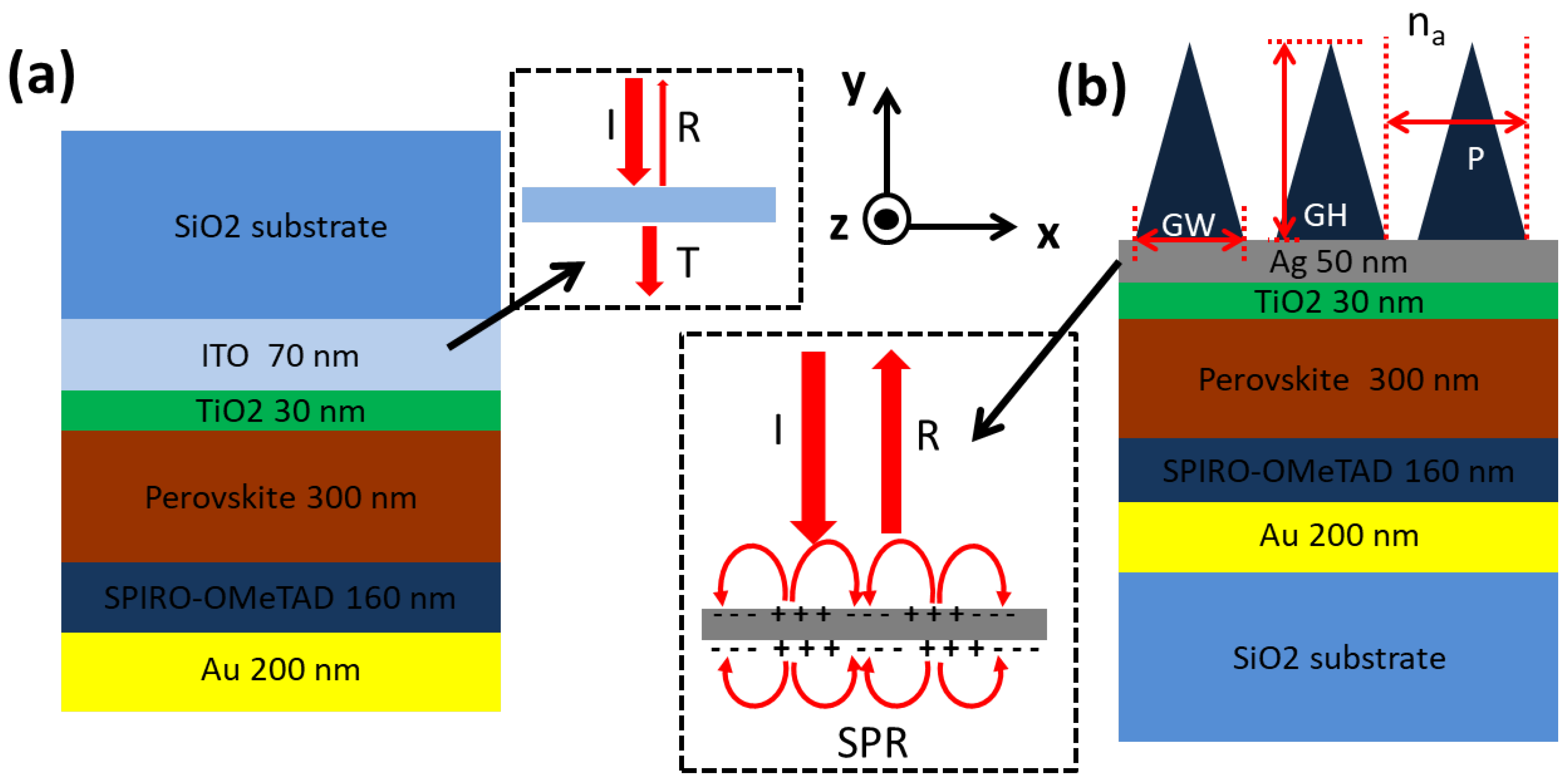
2. Design Parametrization and Methods

A typical perovskite solar cell arrangement has the following structure (from bottom to top): Au [200 nm]/SPIRO OMeTAD [160 nm]/CH 3 NH 3 PbI 3 perovskite [300 nm]/TiO 2 [30 nm]/ITO [70 nm]/SiO 2 substrate/air [23,24], where light is incident from the substrate side (the squared brackets embrace the dimensions of the layers). The layout of this structure is presented in Figure 1a. We modify this structure for sensing application as follows: (i) the SiO 2 substrate moves to the other side, adjacent to the gold layer; (ii) the ITO layer is replaced with a 50 nm-thick silver (Ag) layer (this thickness is optimized for better performance); and (iii) we add an extruded dielectric grating with triangular profile on top of the Ag layer. This nanostructured relief is responsible for the spectral selectivity of the device. The parameters of this nanostructure are its period, P, and the width and height of the triangular shape, GW, and GH, respectively. They will be optimized to maximize the absorption at the active layer maintaining a narrow spectral response for better sensing performance. The triangular nanostructure is made of Si 3 N 4 to have a favorable contrast in the index of refraction of the medium under test (in this case, the sensed material is air). Therefore, the modified structure is (from bottom to top): SiO 2 substrate/Au [200 nm]/SPIRO OMeTAD [160 nm]/CH 3 NH 3 PbI 3 perovskite [300 nm]/TiO 2 [30 nm]/Ag [50 nm]/Si 3 N 4 [P, GW, GH]/air (see Figure 1). The insets in Figure 1 represent the mechanism at play in both designs. In the standard arrangement, ITO works as an antireflection coating and as an electrode to extract the photo-generated current from the device. The silver layer in the modified design works as a reflector and rejects most of the incoming radiation except those wavelengths where the nanostructure generates a SPR [25,26]. These resonances result in strong absorption peaks at the active layer of the cell. Moreover, this absorption is very sensitive to refractive index changes of the medium on top of the grating, i.e., air.
In this contribution, we have used the FEM package COMSOL Multiphysics to evaluate the field distribution, and the reflection and absorption losses within different layers at the cell. A transverse magnetic polarized light (TM) was set for the incident field with an amplitude of 1 A/m, oriented along the Z axis.

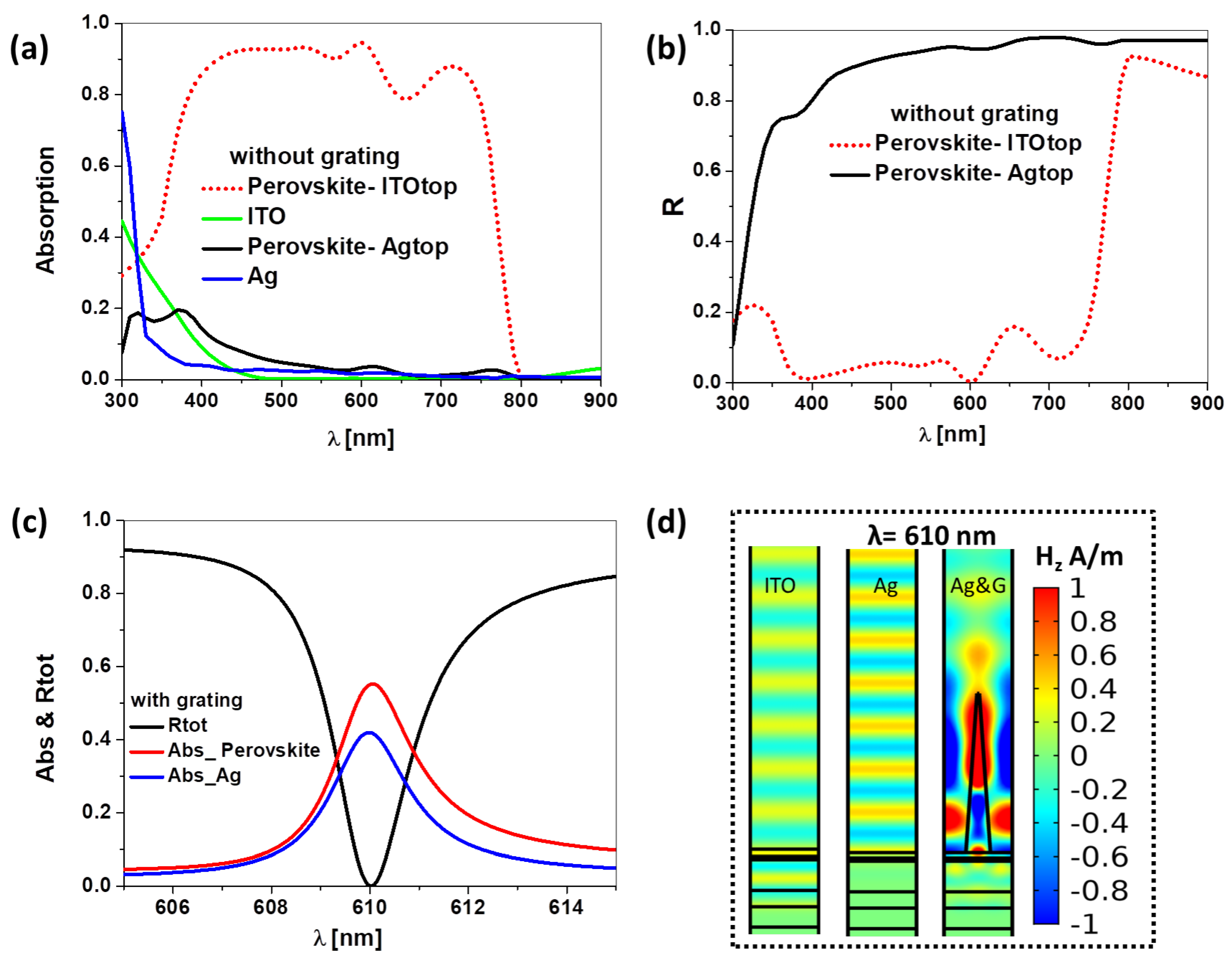
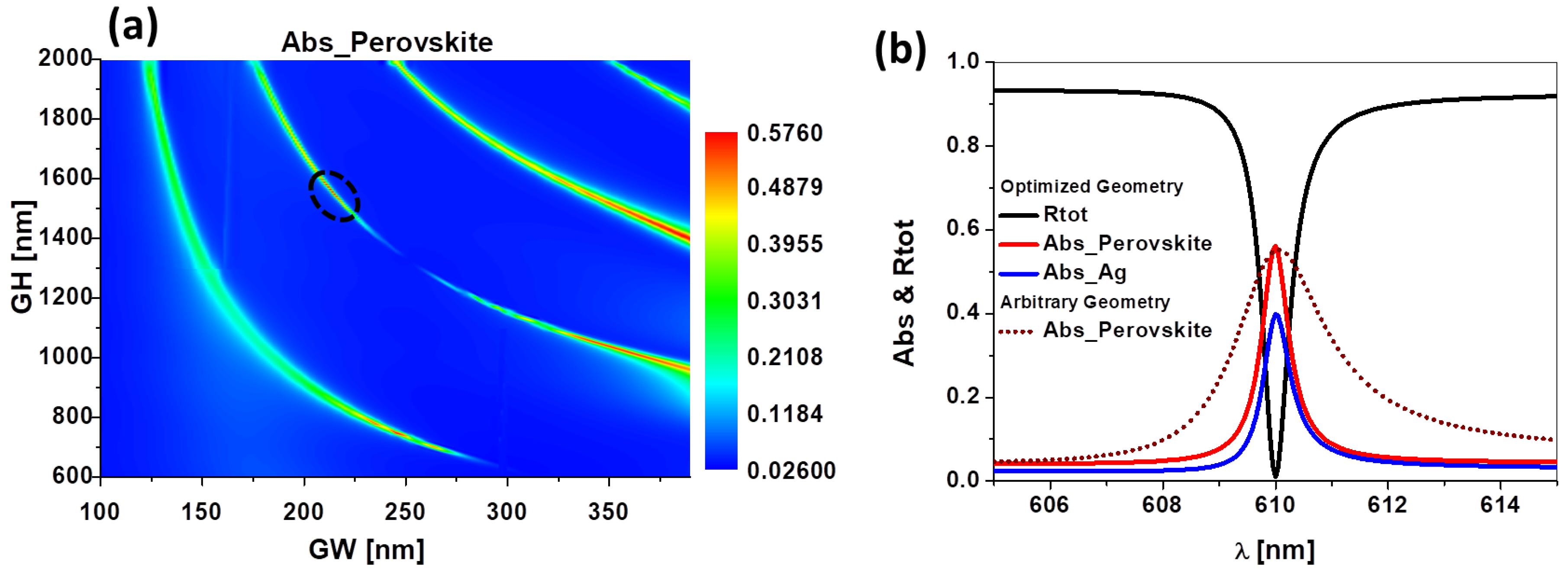
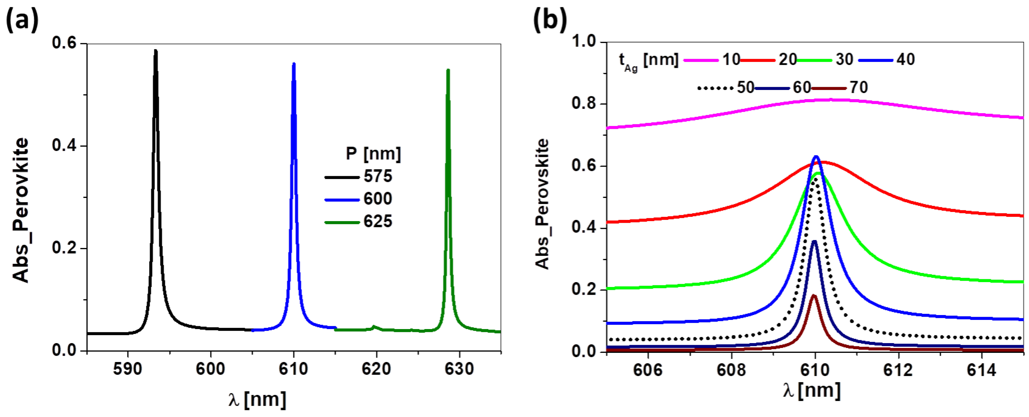
3. Results and Discussion

To begin with, we compare the spectral responses of the standard and modified designs. This evaluation shows how the standard perovskite solar cell is well suited for energy harvesting, meanwhile the modified design shows spectral features applicable to sensing. Actually, the modified design needs further optimization to maximize the coupling of the incident radiation to the SPR, and the availability of this resonance to generate photo-currents at the active layer. As far as the SPR is affected by a change in the refractive index, the absorption at the active layer will also reflect those changes.

3.1. Responses and Optimization

From Figure 2a, perovskite solar cells with ITO contacts show high optical absorption at the active layer (red dashed line) within most of the visible spectrum. The losses are mainly due to reflection and parasitic absorption in different layers. As an example, the absorption of the ITO electrode is represented as a green solid line. This figure also compares the behavior of the standard structure when the transparent electrode is replaced with a silver one (50 nm-thick) that reflect most of the incoming light, and account for some absorption mainly at lower wavelngth in the range 300–400 nm (see blue solid line in Figure 2a. Accordingly, the absorption at the perovskite layer drops, precluding the use of the cell as an energy harvesting device (see black solid line in Figure 2a). The reflectance of the structure for the standard design is represented in Figure 2b as a red dashed curve. We have also plotted the reflectance of the cell when the ITO electrode is replaced with a silver layer (50 nm-thick) on top of the TiO 2 layer, Again, we can see how this metallic layer strongly disturbs the performance of the structure as a energy harvesting device. In Figure 2a,b, neither of the structures contain the pyramidal dielectric grating.
The previous spectral behavior changes when including the effect of the dielectric grating. As a matter of fact, we have selected an spectral region where the perovskite cell absorbs the most ( λ = 610 nm). Now we add a Si 3 N 4 pyramidal grating with geometrical parameters: P = 600 nm, GW = 350 nm, and GH = 1050 nm. The results for the absorption and reflectance are plotted in Figure 2c around λ = 610 nm. The reflectance reaches an almost null value within this range (black solid line), which means a high absorption at the silver and active layers (see red and blue solid lines). These results are confirmed when evaluating the magnetic field distribution (see Figure 2d). These three maps represent the incidence of plane wave under normal incidence conditions and with a wavelength of λ = 610 nm. The plot at the left is for the standard perovskite cell, the map at the middle is for the same cell where ITO is replaced with silver, and the one to the right corresponds with the case of the silver layer plus the dielectric grating. It is worth noting how the field reaches the perovskite layer as hot spots (for the silver plus grating case) instead of a plane wave distribution (when using plane-parallel thin layers).
To improve the capabilities of this device as a refractometric sensor for gases, we perform an optimization of the geometry of the device. This optimization relies on the maximization of the absorption at the active layers of the modified structure and combines a good coupling to the SPR with the device output. Therefore, the merit function is defined as:
MF = A active layer .
At the same time, when maximizing the absorption at the perovskite layer, the lineshape becomes narrower, what is good to increase both sensitivity and the figure of merit of the device taken as a sensor. This optimization is made by changing the profile of the triangular dielectric grating using parameters GW and GH for a fixed period P = 600 nm. We will also fix the wavelength of interest at λ = 610 nm. The parameter P is left for additional tuneability of the device. After obtaining the optimum profile parameters of the grating, we will make a refinement of the design in terms of the thickness of the silver layer.

3.1.1. Optimization

The merit function map in terms of the geometrical parameters of the grating (GW and GH) is presented in Figure 3a, It shows regions where the merit function reaches a high absorption at the perovskite layer. If we plot reflectance, we obtain a similar map with the same regions showing minimum reflectivity. The black circle in Figure 3a locates the highest absorption for the selected wavelength. The value is 57% in absorption at the active layer. This high value is due to SPR. Actually, this result contrast with the 4% in absorption when only a silver layer replace the ITO electrode (without dielectric grating). The geometrical parameters for this maximum in the merit function are: GW = 215 nm and GH = 1560 nm. The tolerance that maintains almost the same values is ±25 nm that could be achieved easily using the available lithographic techniques.
The absorption in the Ag and perovskite layers, and the total reflectance are shown in Figure 3b for the optimized geometry. To better understand the effect of the optimization, we have also plotted the absorption at the perovskite layer for the non-optimized values (see dotted line) used in Figure 2c. Although the intensity has not increased significantly, we can see how the lineshape is much narrower in the optimized case. This will be of importance when evaluating the system as a refractometric sensor.
It is important to check the capability to tune the response at different wavelengths in order to adjust the device using available commercial light sources or to detect at a specific detection band. We fix all the parameters except the period of the grating P, and we only change the grating period. As expected, Figure 4a show a blue shifting when reducing P, and a red-shifting when increasing it. As far as perovskite solar cells have a wide absorption band that covers the VIS-NIR (typically from 300 nm to 800 nm), we can use the period P to tune the response to any desired wavelength in this band.
The metal thickness, t Ag , is an important parameter of the device. Figure 4b shows the absorption within the perovskite layer. We can see how the top contact becomes almost transparent when the silver layer is 10 or 20 nm thick. In these conditions, the SPR does not reveal itself in the lineshape. This happens with thicker silver layers. Actually, the peak in absorption becomes spectrally narrower as the thickness of the metal increases. However, a thick silver layer is not practical because it blocks the light coming to the perovskite layer. In this sense, we choose a thickness for Ag as t Ag = 50 nm because at this value we have both high absorption and narrow response. A thickness of 40 nm could achieve a little better absorption but the linewidth is wider than the case of 50 nm thickness.

3.1.2. Device Performance

Sensitivity and figure of merit (FOM) are two important parameters used to quantify the optical sensor’s performance and to allow comparison with other sensing technologies. The sensitivity is defined as the shift of the optical response with respect to the change in a given environmental parameter. The optical response, related to reflection, absorption and transmission, could be used to sense environmental parameters, as concentration, color or temperature. In this contribution, we aim to sense the change in refractive index of the medium in contact with the nanostructured grating and the metallic layer, for example due to exposure of a gas. If we use optical interrogation, the sensitivity is defined as the shift in the wavelength of the reflection dip caused by refractive index change [27,28]:
S B = Δ λ Δ n ,
where S B is the sensitivity and Δ λ is the wavelength shift due to refractive index change Δ n . The associated figure of merit (FOM) will be [27,28]:
FOM = S B FWHM ,
where FWHM is the full width at half maximum of the reflection response line. Our goal is to optoelectronically interrogate the device. Therefore, we need another opto-electrical term that is the responsivity, R , which is defined as [29]:
R S ( λ ) = I photo P input ( λ ) ,
where I photo is the ideal photo-generated current, and P input ( λ ) is the incident light power that is delivered by a tunable source. The ideal photo-generated current could be optically calculated as in our previous work [20,21]. The sensitivity and FOM will be calculated using Equations (2) and (3), but the wavelength shift will be for the reponsivity dip instead of the reflectivity dip to replace the optical interrogation with an opto-electronic one.
The responsivity of the optimized device is very narrow in wavelength due to the SPR resonance coupled to the absorption in the active layer, we plot the responsivity for different values of refractive index in Figure 5a, ranging from 1 to 1.1, which represents an air medium that is perturbed by some external mechanism (change in concentration, temperature, composition, etc.). The decrease in responsivity when n a increases is caused by our optimization procedure that maximized the absorption at the perovskite active layer for a value of n a = 1.0. Therefore, if the index of refraction of the analyte changes, the design is no longer optimum and the effect is a lower responsivity. Due to their origin as plasmonic resonances, the spectral responsivity can be fitted to Lorentzian lineshapes. An important result of this fitting is the FWHM of the resonance. We have found that FWHM varies from 0.54 nm to 0.68 nm, reaching its minimum value when n a = 1.1. After evaluating these parameters we can obtain the Sensitivity, S B , and the FOM using Equations (2) and (3). These calculations provide a maximum sensitivity of S B , max = 546 nm/RIU and a FOM max = 1005 RIU 1 obtaining both maxima for an index of refraction of n a = 1.1. The minimum values of these parameters along the studied range of the index of refraction are S B , min = 490 nm/RIU (at n a = 1.0), and FOM min = 715 RIU−1 (at n a = 1.03).
The resonance wavelength, which shift when the refractive index change, is nearly linear as seen from Figure 5b and the linear fitting provides a value of S B , linear = 513 nm/RIU. Along with the simple and low-cost optoelectronic interrogation at normal incident conditions compared with the optical-angular interrogation, the device high sensitivity and high FOM values are comparable with many recent reported optical sensors with high sensitivity [30,31,32,33,34].

4. Conclusions

A modified design of perovskite ITO-free solar cells with a metallic-dielectric grating nanostructured electrode is optimized for sensing applications. The excitation of the SPRs coupled to a dielectric diffraction grating produces a very narrow absorption in the active layer of the solar cell, and the same behavior translate to its spectral responsivity. By applying this approach to a well-known photonic platform we take advantage of a mature technology in terms of cost and reliability. The proposed layer arrangement can be deposited on any substrate allowing the design of flexible sensors. The device is operated at normal incidence conditions with a collinear set-up that overcomes the prism coupling requirement of conventional angularly interrogated plasmonic sensors. The response of the sensor can be tuned through a wide spectral band in the visible and NIR where the perovskite absorbs and conventional light sources are available. The optoelectronic interrogation is a simpler alternative to the optical method that replaces the expensive spectrometers parts of the measurement with electrical instrumentation to measure photo-currents. The performance parameters defined in terms of the optoelectronic response compare very well with those obtained from similar sensors spectrally interrogated. This approach has been applied to a refractometric sensor for gases, and the involved geometrical parameters and material were selected considering fabrication constrains of lithographic and nano-imprint techniques.

Author Contributions

Conceptualization: all authors; methodology: all authors; software: M.H.E.; validation: A.C., and J.A.; formal analysis: all authors; investigation: all authors; resources: J.A.; data curation: all authors; writing—original draft preparation: all authors; writing—review and editing: all authors; visualization: M.H.E.; supervision: J.A.; project administration: J.A.; funding acquisition: J.A.

Funding

This research received no external funding.

Acknowledgments

M Elshorbagy thanks the Ministry of Higher Education of Egypt (missions section) for their supporting grant.

Conflicts of Interest

The authors declare no conflict of interest.

Abbreviations

The following abbreviations are used in this manuscript:
SPRSurface plasmon resonance
FOMFigure of merit
FWHMFull width at half maximum

References

  1. Bingham, J.M.; Anker, J.N.; Kreno, L.E.; Van Duyne, R.P. Gas Sensing with High Resolution Localized Surface Plasmon Resonance Spectroscopy. J. Am. Chem. Soc. 2010, 132, 17358–17359. [Google Scholar] [CrossRef] [PubMed]
  2. Vila, A.G.; Ioannou, A.; Loyez, M.; Debliquy, M.; Lahem, D.; Caucheteur, C. Surface plasmon resonance sensing in gaseous media with optical fiber gratings. Opt. Lett. 2018, 43, 2308–2311. [Google Scholar] [CrossRef] [PubMed]
  3. Jung, I.; Ih, S.; Jung, S.; Yoo, S.; Park, S. Tricomponent Multiblock Nanorods for Fourier Transform Surface Plasmon Resonance and Its Chemical Sensing. Anal. Chem. 2019, 91, 5494–5498. [Google Scholar] [CrossRef] [PubMed]
  4. Chah, S.; Hammond, M.R.; Zare, R.N. Gold Nanoparticles as a Colorimetric Sensor for Protein Conformational Changes. Chem. Biol. 2005, 12, 323–328. [Google Scholar] [CrossRef] [PubMed]
  5. Farmani, H.; Farmani, A.; Biglari, Z. A label free graphene-based nanosensor using surface plasmon resonance for biomaterials detection. Phys. E Low-Dimens. Syst. Nanostruct. 2020, 116, 113730. [Google Scholar] [CrossRef]
  6. Prabowo, B.; Purwidyantri, A.; Liu, K.C. Surface plasmon resonance optical sensor: A review on light source technology. Biosensors 2018, 8, 80. [Google Scholar] [CrossRef]
  7. Lee, T.W.; Gray, S.K. Remote grating-assisted excitation of narrow-band surface plasmons. Opt. Express 2010, 18, 23857–23864. [Google Scholar] [CrossRef]
  8. Dhawan, A.; Canva, M.; Vo Dinh, T. Narrow groove plasmonic nano-gratings for surface plasmon resonance sensing. Opt. Express 2011, 19, 787–813. [Google Scholar] [CrossRef]
  9. Polyakov, A.; Thompson, K.; Dhuey, S.; Olynick, D.; Cabrini, S.; Schuck, P.; Padmore, H. Plasmon resonance tuning in metallic nanocavities. Sci. Rep. 2012, 2, 933. [Google Scholar] [CrossRef]
  10. Sun, M.; Sun, T.; Liu, Y.; Zhu, L.; Liu, F.; Huang, Y.; Chang-Hasnain, C. Integrated plasmonic refractive index sensor based on grating/metal film resonant structure. High Contrast Metastruct. V Int. Soc. Opt. Photonics 2016, 9757, 97570Q. [Google Scholar]
  11. Elshorbagy, M.H.; Cuadrado, A.; Alda, J. Plasmonic Sensor Based on Dielectric Nanoprisms. Nanoscale Res. Lett. 2017, 12, 580. [Google Scholar] [CrossRef] [PubMed]
  12. Elshorbagy, M.H.; Cuadrado, A.; Alda, J. High sensitivity integrated devices based on surface plasmon resonance for sensing applications. Photonics Res. 2017, 5, 654–661. [Google Scholar] [CrossRef]
  13. Elshorbagy, M.H.; Cuadrado, A.; Gonzalez, G.; Gonzalez, F.J.; Alda, J. Performance Improvement of Refractometric Sensors Through Hybrid Plasmonic Fano Resonances. J. Light. Technol. 2019, 37, 2905–2913. [Google Scholar] [CrossRef]
  14. Qin, L.; Zhang, C.; Li, R.; Li, X. Silicon-gold core-shell nanowire array for an optically and electrically characterized refractive index sensor based on plasmonic resonance and Schottky junction. Opt. Lett. 2017, 42, 1225–1228. [Google Scholar] [CrossRef]
  15. Green, M.A.; Ho Baillie, A.; Snaith, H.J. The emergence of perovskite solar cells. Nat. Photonics 2014, 8, 506. [Google Scholar] [CrossRef]
  16. Tai, Q.; Tang, K.C.; Yan, F. Recent progress of inorganic perovskite solar cells. Energy Environ. Sci. 2019, 12, 2375–2405. [Google Scholar] [CrossRef]
  17. Zeng, Q.; Zhang, X.; Liu, C.; Feng, T.; Chen, Z.; Zhang, W.; Zheng, W.; Zhang, H.; Yang, B. Inorganic CsPbI2Br Perovskite Solar Cells: The Progress and Perspective. Sol. RRL 2019, 3, 1800239. [Google Scholar] [CrossRef]
  18. Roghabadi, F.A.; Alidaei, M.; Mousavi, S.M.; Ashjari, T.; Tehrani, A.S.; Ahmadi, V.; Sadrameli, S.M. Stability progress of perovskite solar cells dependent on the crystalline structure: From 3D ABX 3 to 2D Ruddlesden–Popper perovskite absorbers. J. Mater. Chem. A 2019, 7, 5898–5933. [Google Scholar] [CrossRef]
  19. Zhao, Y.; Ye, Q.; Chu, Z.; Gao, F.; Zhang, X.; You, J. Recent Progress in High-efficiency Planar-structure Perovskite Solar Cells. Energy Environ. Mater. 2019, 2, 93–106. [Google Scholar] [CrossRef]
  20. Elshorbagy, M.H.; Alda, J. Funneling and guiding effects in ultrathin aSi-H solar cells using one-dimensional dielectric subwavelength gratings. J. Photonics Energy 2017, 7, 017002. [Google Scholar] [CrossRef]
  21. Elshorbagy, M.; Abdel-Hady, K.; Kamal, H.; Alda, J. Broadband anti-reflection coating using dielectric Si3N4 nanostructures. Application to amorphous-Si-H solar cells. Opt. Commun. 2017, 390, 130–136. [Google Scholar] [CrossRef]
  22. Mukti, R.J.; Hossain, M.R.; Islam, A.; Mekhilef, S.; Horan, B. Increased absorption with Al nanoparticle at front surface of thin film silicon solar cell. Energies 2019, 12, 2602. [Google Scholar] [CrossRef]
  23. Vivo, P.; Salunke, J.K.; Priimagi, A. Hole transporting materials for printable perovskite solar cells. Materials 2017, 10, 1087. [Google Scholar] [CrossRef] [PubMed]
  24. Kim, J.; Ho Baillie, A.; Huang, S. Review of Novel Passivation Techniques for Efficient and Stable Perovskite Solar Cells. Sol. RRL 2019, 3, 1800302. [Google Scholar] [CrossRef]
  25. Hu, C.; Liu, D. High performance grating coupled surface plasmon resonance sensor based on Al Au Bimetallic layer. Mod. Appl. Sci. 2010, 4, 8. [Google Scholar] [CrossRef]
  26. Babaei, E.; Sharifi, Z.; Gordon, R. Improving sensitivity of existing surface plasmon resonance systems with grating coupled short range surface plasmons. JOSA B 2019, 36, F144–F148. [Google Scholar] [CrossRef]
  27. Homola, J. On the sensitivity of surface plasmon resonance sensors with spectral interrogation. Sens. Actuators B Chem. 1997, 41, 207–211. [Google Scholar] [CrossRef]
  28. van Gent, J.; Lambeck, P.V.; Kreuwel, H.J.; Gerritsma, G.J.; Sudholter, E.J.; Reinhoudt, D.N.; Popma, T.J. Optimization of a chemooptical surface plasmon resonance based sensor. Appl. Opt. 1990, 29, 2843–2849. [Google Scholar] [CrossRef]
  29. Gan, X.; Shiue, R.J.; Gao, Y.; Meric, I.; Heinz, T.F.; Shepard, K.; Hone, J.; Assefa, S.; Englund, D. Chip integrated ultrafast graphene photodetector with high responsivity. Nat. Photonics 2013, 7, 883. [Google Scholar] [CrossRef]
  30. Klos, G.; Miola, M.; Sutherland, D.S. Increased Refractive Index Sensitivity by Circular Dichroism Sensing through Reduced Substrate Effect. J. Phys. Chem. C 2019, 123, 7347–7355. [Google Scholar] [CrossRef]
  31. Muhammad, N.; Ouyang, Z.; Liu, Q.; Tang, X.; Deng, Z.L.; Daud Khan, A. Sensitive label-free sensor with high figure of merit based on plasmonic metasurface with unit cell of double two-split nanorings. J. Mater. Sci. 2019, 54, 6301–6309. [Google Scholar] [CrossRef]
  32. Alipour, A.; Farmani, A.; Mir, A. High sensitivity and tunable nanoscale sensor based on plasmon induced transparency in plasmonic metasurface. IEEE Sens. J. 2018, 18, 7047–7054. [Google Scholar] [CrossRef]
  33. Kim, S.; Lee, Y.; Kim, J.Y.; Yang, J.H.; Kwon, H.J.; Hwang, J.Y.; Moon, C.; Jang, J.E. Color sensitive and spectrometer free plasmonic sensor for biosensing applications. Biosens. Bioelectron. 2019, 126, 743–750. [Google Scholar] [CrossRef] [PubMed]
  34. Yin, B.; Wu, S.; Wang, M.; Liu, W.; Li, H.; Wu, B.; Wang, Q. High sensitivity refractive index and temperature sensor based on cascaded dual -wavelength fiber laser and SNHNS interferometer. Opt. Express 2019, 27, 252–264. [Google Scholar] [CrossRef] [PubMed]
Figure 1. (a) Standard perovskite material arrangement. (b) Modified design for sensing applications, where the top ITO contact is replaced with an Ag layer and a dielectric grating with triangular shape with the top medium above the cell with refractive index n a . In both cases, light is coming from top oscillating in Z direction and propagating in Y direction, the 2D cross section of the structure is contained in the X Y plane, as seen the the coordinate inset in the top middle. The insets in dashed rectangles show the mechanisms at play in this structures.
Applsci 09 04850 g001
Figure 2. (a) Optical absorption in the active layer and top contact for the planer perovskite solar cells. (b) Spectral reflection for this two planer cases without grating. (c) The absorption in perovskite layer (red line), absorption in Ag top contact (blue line) and the total reflectance of the whole device (black line) for the proposed design with Ag-grating layer. (d) Magnetic field maps for the device with ITO (left), Ag only (middle), and Ag+grating (right) at the resonance wavelength λ = 610 nm, showing how light reaches the active layer only in the case of ITO and Ag+grating. The case with Ag only does not transmit light to the active layer significantly.
Applsci 09 04850 g002
Figure 3. (a) Optical absorption in the perovskite layer with the grating parameters GW, and GH for a fixed Period P 600 nm at a single wavelength at, λ = 610 nm, using TM polarized light of 1 A/m amplitude the highlighted black dashed circle defines the location of the point where the absorption in perovskite is maximized. (b) The absorption in perovskite layer (red line), absorption in Ag top contact (blue line), the total reflectance of the whole device (black line) for the optimized geometry, and the absorption in perovskite layer (brown dashed line) for the arbitrarily selected geometry before optimization.
Applsci 09 04850 g003
Figure 4. (a) Effect of the period of the grating P, on the wavelenght of resonance. The resonant wavelength is proportional to the period of the dielectric grating P. (b) Effect of the thickness of the metal layer on the spectral relevance of the SPR. The optimum thickness, t Ag = 50 nm, is plotted as a dashed line.
Applsci 09 04850 g004
Figure 5. (a) Spectral responsivity of the optimized device for different values of the refractive index of the analyte medium, n a . (b) Resonance wavelength in terms of the refractive index change. It shows a linear behavior through the whole scanned refractive index range.
Applsci 09 04850 g005

