Article

Tailored Chip Breaker Development for Polycrystalline Diamond Inserts: FEM-Based Design and Validation

1
Advanced Manufacturing Technologies Unit, IK4-TEKNIKER, 20600 Eibar, Spain
2
Institute for Automation and Applied Informatics, Karlsruhe Institute of Technology, 76344 Karlsruhe, Germany
3
Faculty of Engineering, Port Said University, Port Fuad 42526, Egypt
*
Author to whom correspondence should be addressed.
Appl. Sci. 2019, 9(19), 4117; https://doi.org/10.3390/app9194117
Submission received: 4 July 2019 / Revised: 23 September 2019 / Accepted: 27 September 2019 / Published: 1 October 2019

Abstract

:
Chip evacuation is a critical issue in metal cutting, especially continuous chips that are generated during the machining of ductile materials. The improper evacuation of these kinds of chips can cause scratching of the machined surface of the workpiece and worsen the resultant surface quality. This scenario can be avoided by using a properly designed chip breaker. Despite their relevance, chip breakers are not in wide-spread use in polycrystalline diamond (PCD) cutting tools. This paper presents a systematic methodology to design chip breakers for PCD turning inserts through finite element modelling. The goal is to evacuate the formed chips from the cutting zone controllably and thus, maintain surface quality. Particularly, different scenarios of the chip formation process and chip curling/evacuation were simulated for different tool designs. Then, the chip breaker was produced by laser ablation. Finally, experimental validation tests were conducted to confirm the ability of this chip breaker to evacuate the chips effectively. The machining results revealed superior performance of the insert with chip breaker in terms of the ability to produce curly chips and high surface quality (Ra = 0.51–0.56 µm) when compared with the insert without chip breaker that produced continuous chips and higher surface roughness (Ra = 0.74–1.61 µm).

1. Introduction

Given their high performance under severe working conditions, via mechanical and thermal stresses and harsh chemical environments [1,2], superalloys and advanced materials have been widely used in the manufacturing of components for jet engines [2], turbochargers [3] and aerospace [4] applications. Nevertheless, these materials display difficult machinability characteristics [5,6] due to their low thermal diffusivity [2], high strain hardening [7], high chemical reactivity [8], carbide precipitation in grain boundaries [1] and high ductility [9]. Chief among these machining attributes, the high ductility of machined workpieces ordinarily leads to the formation of long continuous chips during the machining process, which negatively affects the safety, efficiency and continuity of the machining operation [10].
An appropriately controlled machining process enables high productivity and minimizes costs of energy, materials, and tools [11]. This necessitates restrictive cutting conditions to be identified and rigorously applied [11,12]. In addition, an appropriate design of a cutting tool is essential to achieve an effective chipping operation and to extend tool life [13,14]. However, chip evacuation is a recurrent problem that needs addressing with machining ductile and soft materials, especially with the formation of continuous chips [10,15,16]. Discontinuous and fragmented chips are easier to control as continuous chips can wrap around the workpiece and/or the cutting tool and clog the cutting zone, which negatively affects the cutting process. Such chips can scratch the newly machined surface, detract from its quality and increase tool wear/breakage thereby decreasing tool life [17,18]. This results in a higher number of production stops and, therefore, in a dramatic increase of production time. Thus, the chip formation process and chip control using combined cryogenic and minimum quantity lubrication [19,20], applying cryogenic lubrication [7,21], high pressure coolant [2,11] ultrasonic-assisted vibration [15,17], optimization of the processing parameters [10,22,23,24], and chip breakers [10,14,16] as well as their limitations [25], have been widely studied, both experimentally and by means of simulation.
It is widely accepted that the contribution of chip breakers in enhancing the chip fragmentation process is significant. Chip breakers prolong tool service life and enhance obtainable surface finishing of the component, particularly when it comes to cutting ductile materials [16]. Generally, there are a wide range of carbide-tools with an enormous variety of chip breaker types and shapes commercially available. However, to the best of the authors’ knowledge, this is not the case for polycrystalline diamond (PCD) tools, where there is a gap in the market to offer reliable PCD inserts with chip breakers [25]. Due to its high hardness and high abrasive resistance, PCD inserts are widely used for the high-quality machining of non-ferrous metals such as aluminum alloys [26,27]. Given that aluminum alloys are ductile materials, the machining processes of such materials are associated with the generation of continuous chips that require dependable chip control. In this context, there has been an increasing demand for PCD inserts with chip breakers to satisfy the ongoing requirements of modern machining applications.
Recently, there have been trials by such tool manufacturers as Mitsubishi, Lach Diamond, and others to integrate non-conventional technologies in their production processes in order to introduce chip-breaker geometries in their PCD inserts [28,29]. However, these implants are for standard and general-purpose inserts only, and there are no similar applications for special or custom tools.
When tailoring chip breakers for machining ductile materials, it is important to consider the different breaking mechanisms of the chips generated, founded on the processed material, process parameters and cutting tool geometry. Chips are liable to break spontaneously at the weakest points along their lengths, or against the cutting tool, or against the workpiece surface [30], see Figure 1a–c. The second and third scenarios can damage the tool or surface quality, respectively. This makes it critical to control the chip evacuation process, which can be satisfactorily achieved using proper chip breaker geometry to bend the generated chip sufficiently so that it breaks on its own.
Researchers have studied different methodologies to optimize chip breakers design, experimentally [16] and combining experimentation and simulation [14,31], but most of them restricted their work to non-PCD insert tools. On the other hand, the authors previously worked on developing chip breakers for PCD inserts welded into milling-tools [14]. One of the main issues was the implementation of a simulation tool to model the processing of PCD by a ns-pulsed laser. However, the study was focused on a milling case, and while milling processes generate discontinuous chips, the study did not address the chip evacuation problem.
When turning ductile materials, long continuous chips are generated and they tend to wrap around the part. Accordingly, the motivation for this research study was to carry out a systematic methodology to design customized chip breakers that enable a controlled removal of the chips from the working zone. The proposed approach utilizes finite element method (FEM), due to its high ability to accurately simulate the chipping process [32], taking into account the machining process parameters and the material to be machined.
Following this introduction section, there is a description of the methodology used, based on a finite element (FE) study, to design a customized chip-breaker. After that, the case study of the design a chip breaker for a PCD turning insert is presented, which shows the design process in a practical way. Next, the chip breaker was manufactured by means of laser technologies and real machining tests were conducted. Finally, there is an assessment of the results and, afterwards, conclusions are drawn.

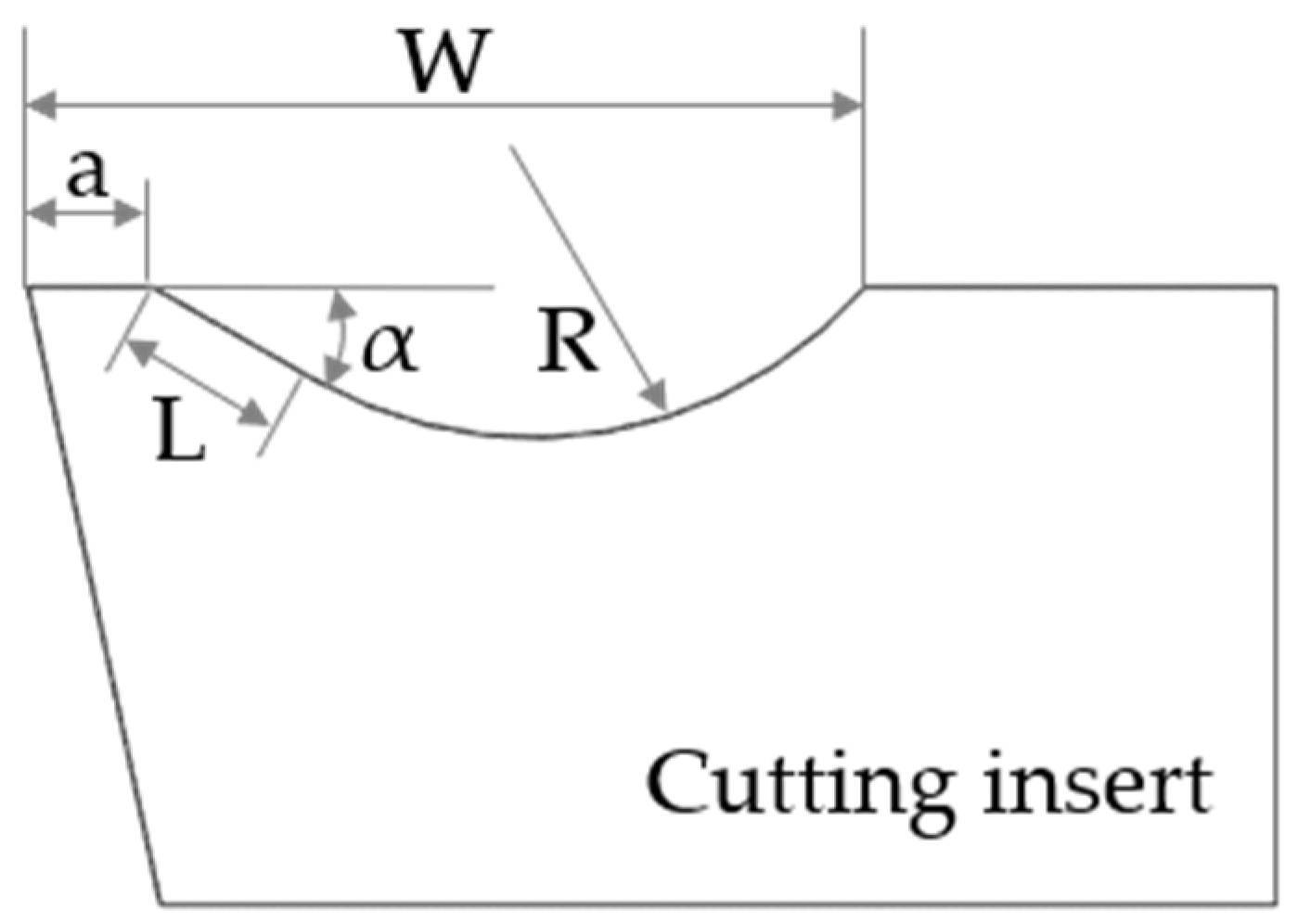
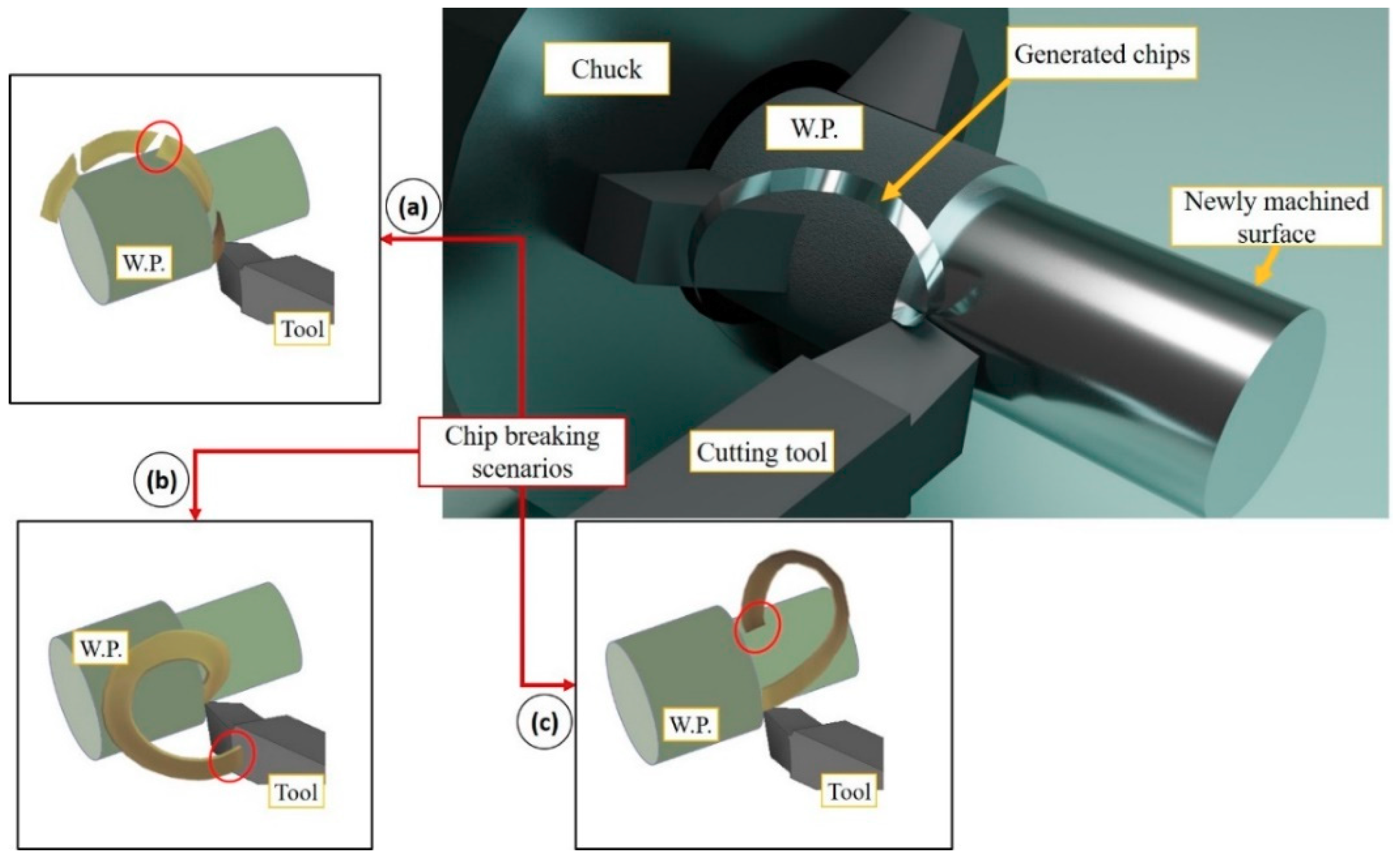
2. Chip Breaker FE Design for a PCD Turning Insert

Although numerous tool manufacturers still base their tool-designs on try-and-see methods based on their previous experience [19], FEM is considered a reliable tool to assess the relative performance of several designs of engineering components, and has been extensively used for the design of cutting tools [32,33,34]. Gurbuz et al. [35] pointed out the significance of FEM to evaluate different design geometries to determine a final design before manufacturing, which is substantially cheaper than trial and error methods.
The first stage of tool design is to identify the relevant geometrical parameters. Sreekala and Sreekala [36] chose a curved groove geometry as the basic design for a chip breaker. This geometry and the nomenclature were followed by other researchers [26,36]. It is expected that including backwall height to the chip breaker geometry would significantly restrict the chip breaker design, especially the radius of curvature. For this reason, conventional curve groove geometry was considered, dismissing the backwall height [36].
Figure 2 shows the essential parameters in the design of the cutting edge of a chip breaker: Rake angle (α); land width (a); radius of curvature (R); and tool-chip contact length (L). The groove width (W), however it is not an independent parameter, but it depends on the aforementioned ones.
The design stage requires: (1) Selection of land width and rake angle; and (2) selection of the radius of curvature. In this study, and regarding the selection of land width and rake angle, several simulations were carried out with combinations of different land widths and rake angles, with the aim of determining the combination that produced the chip with most curl, without a chip breaker. Regarding the selection of the radius of curvature, the curved groove of the chip breaker was tested with different values of the radius of curvature to ascertain the most effective value.
FE simulations were carried out using Third Wave Systems AdvantEdge©, Minneapolis, MN, USA, version 7.2, a commercial software package for simulating machining processes [37]. As a Lagrangian finite-element-based simulation, it can predict the chip formation process, including chip breaking. Furthermore, it enables defining custom geometries of the workpiece and tool and offers a wide range of output parameters such as strain rate, stresses, plastic strain and temperatures.

3. Case Study

For the better understanding of the design process of a chip breaker for a PCD insert, a particular case study for a PCD turning insert is presented. The findings of this case study will be then experimentally validated in real machining tests.
The starting geometry of the turning insert is a rhombic 80° insert CNGA 120408 with a chamfer on the cutting tool edge of 0.1 × 0.07 mm, see Figure 3a,b. Cutting conditions for this study, which belong to the cutting range data recommended by the manufacturer: Depth of cut (Ap) = 1–4 mm and feed (f) = 0.05–0.2 mm/rev, are shown in Table 1. Based on this geometry and cutting conditions, the value of the rake angle, α; land width, a; and radius of curvature, R, will be chosen systematically, considering the results of the FE simulations.

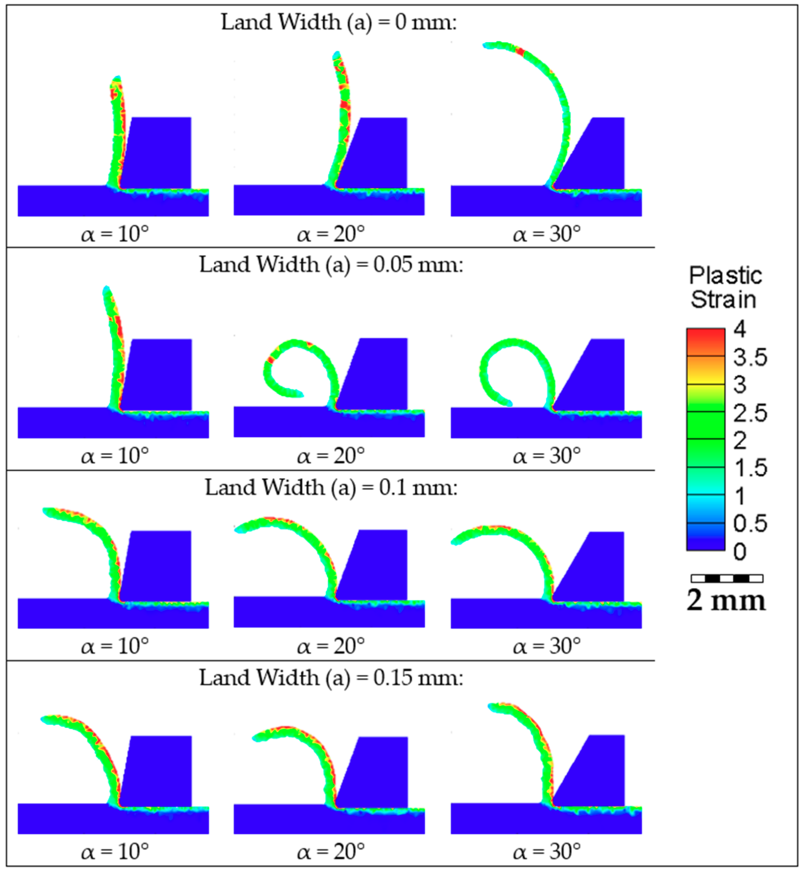
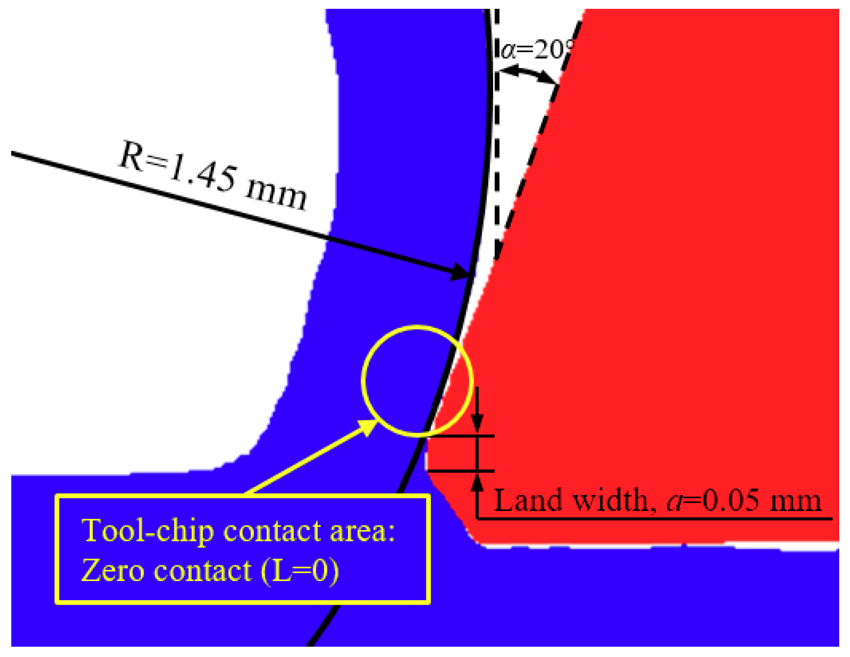
3.1. Selection of Rake Angle (α) and Land Width (a)

For a chip to break spontaneously (see Figure 1a), it is necessary that it curls sufficiently. For that purpose, on this first stage of the design, FE simulations trials were performed to obtain the best combination of rake angle (α) and land width (a) to optimize chip curling without using a chip breaker. These two parameters should not be analyzed independently, as the behavior of the chip during formation near the cutting edge depends on their combination.
Three values of rake angle (α) were proposed: 10°, 20° and 30°. It is assumed that higher rake angles lead to lower cutting forces, so the selection of a positive rake angles [38,39] is recommended. However, there are some drawbacks for excessive rake angles. The key issue is that the higher the rake angle is, the weaker the cutting edge becomes. This fact introduces higher stresses on the cutting insert and leads to higher tool wear. This is because with higher rake angles, the contact area between the tool and the chip is reduced, so the equivalent application-point of the normal force moves towards the cutting edge. Furthermore, this interface between tool and chip is the region of the maximum contact temperature and shifting this towards the cutting edge, shortens the life of the tool, according to Astakhov [40]. Thus, a rake angle over 30° would be inappropriate, as it would excessively weaken the tool edge.
Four values for the land width (a) were proposed according to the feed rate: Non-existent land width, a = 0.00 mm; a = 0.05 mm, equal to 50% of the feed rate; land width equal to the feed rate, a = 0.1 mm; and a = 0.15 mm, 1.5 times the feed rate.
The results obtained from the FE simulation are shown in Table 2 and Figure 4. The best solution corresponds to a rake angle of α = 20° and a land width a = 0.05 mm, that is 50% of the feed rate. This combination gives the lowest radius of curvature of the generated chip without using chip breaker, as well as considerably lowering the cutting forces and temperatures. Consequently, this was the design selected for the chip breaker’s edge in the first stage.

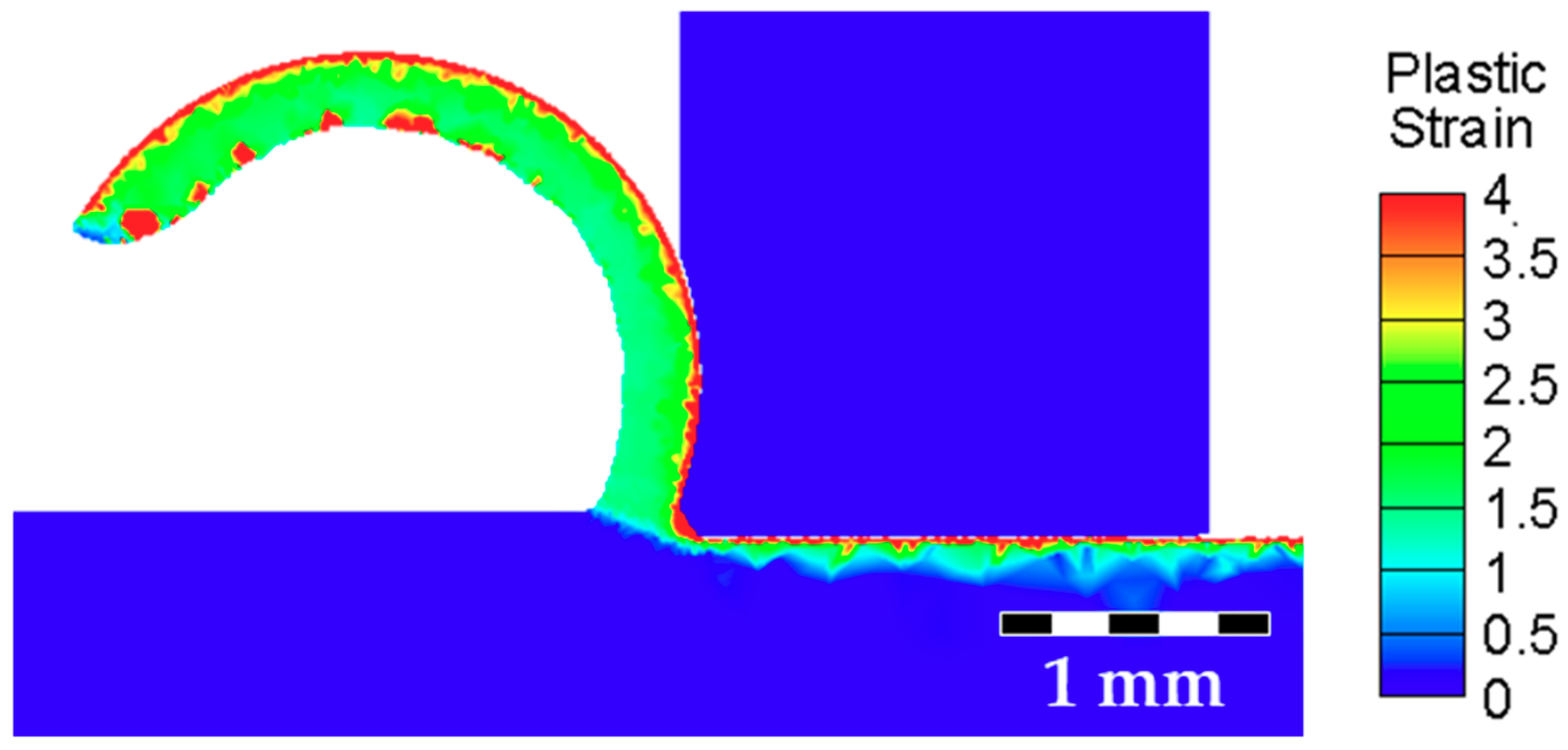
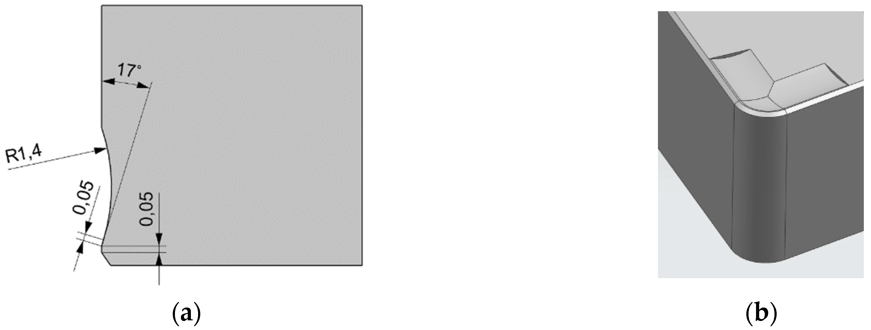
3.2. Determination of the Radius of Curvature

Once the optimum land width and rake angle are selected, the next step is to determine a proper curvature that enables curling the chips without getting clogged. From the previous simulation in which no chip breaker was considered, with α = 20° and a = 0.05 mm, the natural radius of curvature (R) obtained was 1.45 mm and the tool-chip contact length (L) was zero, measured from the land width (i.e., L = 0, see Figure 5). These two parameters are interrelated and, when adding the chip breaker, they will determine the tool-chip contact area.
Regarding L, generally, the value of this parameter in the chip breaker design should be the same or lower than the natural tool-chip contact length, in order to increase chip curling. However, due to manufacturing issues, a minimum value of L should be stablished. Thus, although from simulation it was obtained that L = 0, on this stage of the chip breaker design, L was given a non-zero value, namely 0.05 mm, to ease manufacturing task.
The radius (R) of the chip breaker must be selected bearing in mind the chip’s natural shape in order to increase chip curling, for the chips breaking more readily. As the natural radius of curvature without chip breaker was 1.45 mm, R of the chip breaker must be lower. There is a threshold for R that is determined as, under this value, the chips are prone to get clogged and turning efforts are triggered. Figure 6 reveals how the chip curled for two different values of R, both of them lower than the natural curvature: 1.0 and 1.4 mm. Results show that the lowest one, that is R = 1 mm, was below the threshold value, as seen in Figure 6a. As the shearing angle was reduced, the chip thickness increased, and the chip tended to be relatively straight. Therefore, this is not an admissible solution. For R = 1.4 mm, the chip curled without clogging, this being a suitable solution. Thus, to machine the material considering the cutting parameters in Table 1, a radius greater than 1.0 and equal or lower than 1.4 mm is needed.
FEM simulation is a very powerful, reliable and cheap way of evaluating the cutting geometries. However, as modelling is a simplification of the reality, it is recommended that selected values for critical parameters of the design consider a security margin. Thus, as the gap between R being 1.0 mm or 1.4 mm is very small, instead of searching for an exact intermediate threshold value, the most conservative option was selected: R = 1.4 mm.
Considering the dimensions of the diamond tip, geometrical constraints of the top surface of the original PCD insert have to be taken into consideration during the design phase. In fact, a limited groove width of 1 mm (see Figure 2) can be fabricated. Besides this, and due to limitation of laser manufacturing process, the depth of the groove should not be larger than 100 μm. With α = 20°, a = 0.05 mm, L = 0.05 mm and R = 1.4 mm, these limits are slightly exceeded, so the design must be marginally modified to meet the requirements. From the FE simulation study in the first stage, it was concluded that minor modifications on the land width could drastically change the curling effect of the chip. Therefore, the land width (a) should not be modified. In the same way, regarding R, there was a small gap between the selected and the threshold value, so R will be maintained to avoid clogging. As for L, a minimum value of 0.05 mm was selected for manufacturing reasons, so it cannot be reduced. Thus, the only parameter suitable to be slightly modified is the rake angle.
The new rake angle (which should be as similar as possible to 20°) which meets the requirements is α = 17°. The geometry of the chip breaker obtained from the FE modelling work is shown in Figure 7a,b with rake angle (α) of 17°, radius of curvature of 1.4 mm, land width (a) of 0.05 mm, with overall groove width of 1.0 mm and a maximum depth of 76 μm.
Using the final chip breaker geometry, as displayed in Figure 7, with the machining conditions shown in Table 1, a final simulation was conducted. The result, presented in Figure 8, shows an acceptable chip curling, with a radius of curvature corresponding to R = 1.4 mm, without clogging.

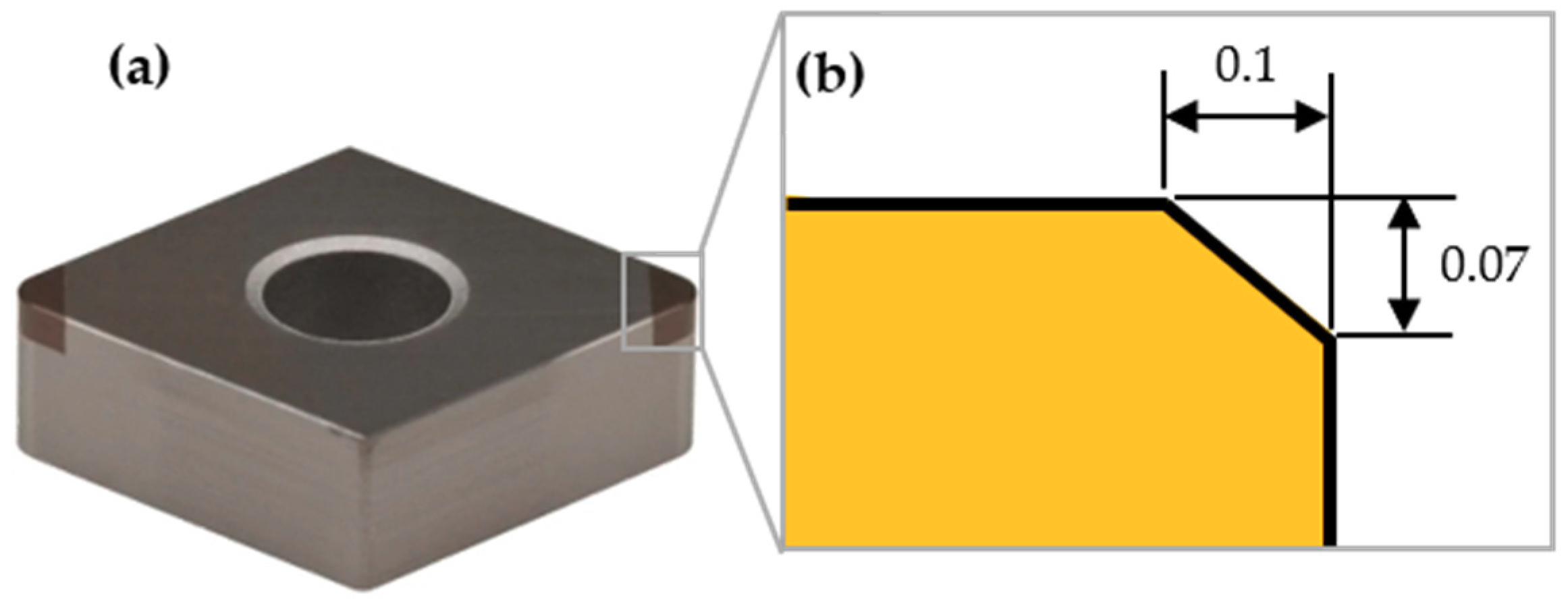
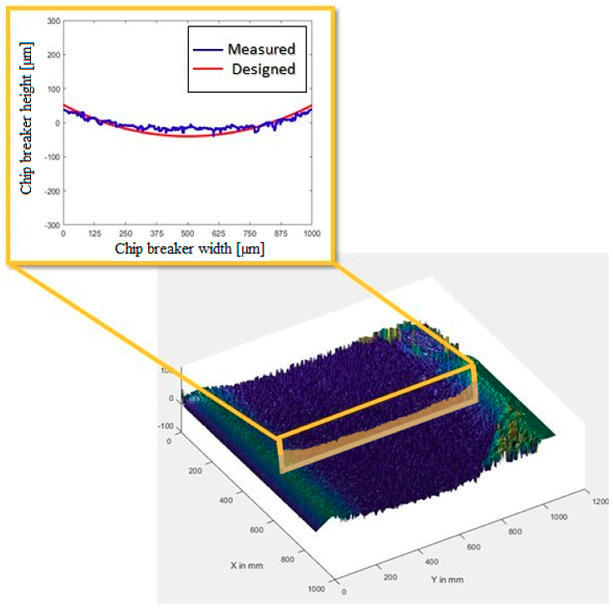
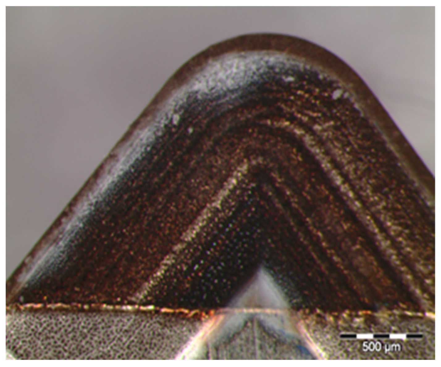
3.3. Manufacturing of the Chip Breaker

The chip breaker was manufactured using a nano-second laser, the ablation process was performed with a SPI-G4-HS ns ytterbium-doped fiber laser, Hedge End, Southampton, United Kingdom, emitting pulses at a wavelength of 1064 nm and using a mean power value of around 40 W. It has been reported that the ablation of PCD using ns pulses takes place via graphitization of the diamond in the PCD which is transformed into graphitic carbon [41]. The proportionality between the graphite-layer thickness, the pulse duration and the laser fluence has been proven [42]. To minimize the thickness of this unwanted graphite-layer, the pulse duration and the fluence of the laser pulses to process the PCD were as low as possible.
Initial experimental trials were conducted over a PCD turning-insert by ablating overlapping trenches under the minimum fluence of 23.74 J/cm2, pulse duration of 40 ns for scanning velocities varying from 0.6 m/s to 1.0 m/s, with overlapping distance between parallel trenches from 5 to 20 µm.
The chip breaker geometry was produced by ablating sequential layers, but it is well known that the resultant surface roughness is higher when layers are thicker. Thus, in order to minimize surface roughness, the thickness of the layers was chosen to be less than 4.0 µm. The results of the preliminary experiments showed that when ablating parallel trenches under 0.8 m/s scanning speed and 10 µm of overlap distance between parallel trenches, the ablated-layer thickness was among 3.6–4.0 µm. As a result, the concluding chip breaker contour was divided into 20 layers and fed into the laser software to be ablated sequentially using the identified optimum parameters. Figure 9 illustrates the geometry of the chip breaker after the laser manufacturing process. The ablated geometry of the chip breaker was measured, as seen in Figure 10, using a confocal 3D optical profiler, S NEOX by SENSOFAR Metrology, Terrassa, Barcelona, Spain. The results revealed a good agreement (with 6% error) between the measured and designed width of the chip breaker. However, a higher discrepancy of 14% was detected for the produced depth of the ablated chip breaker when compared with the designated geometry.

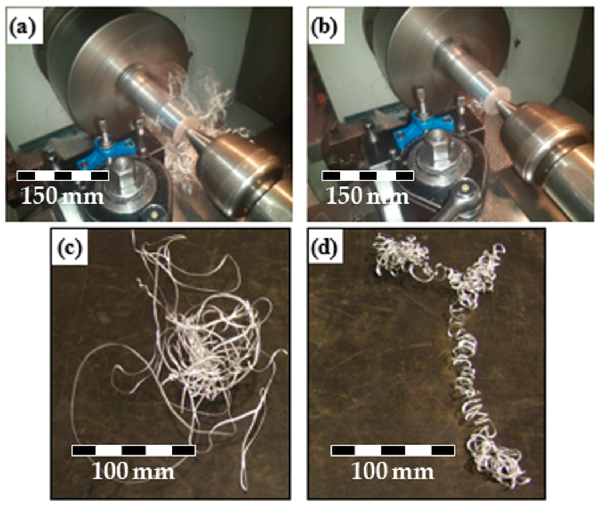
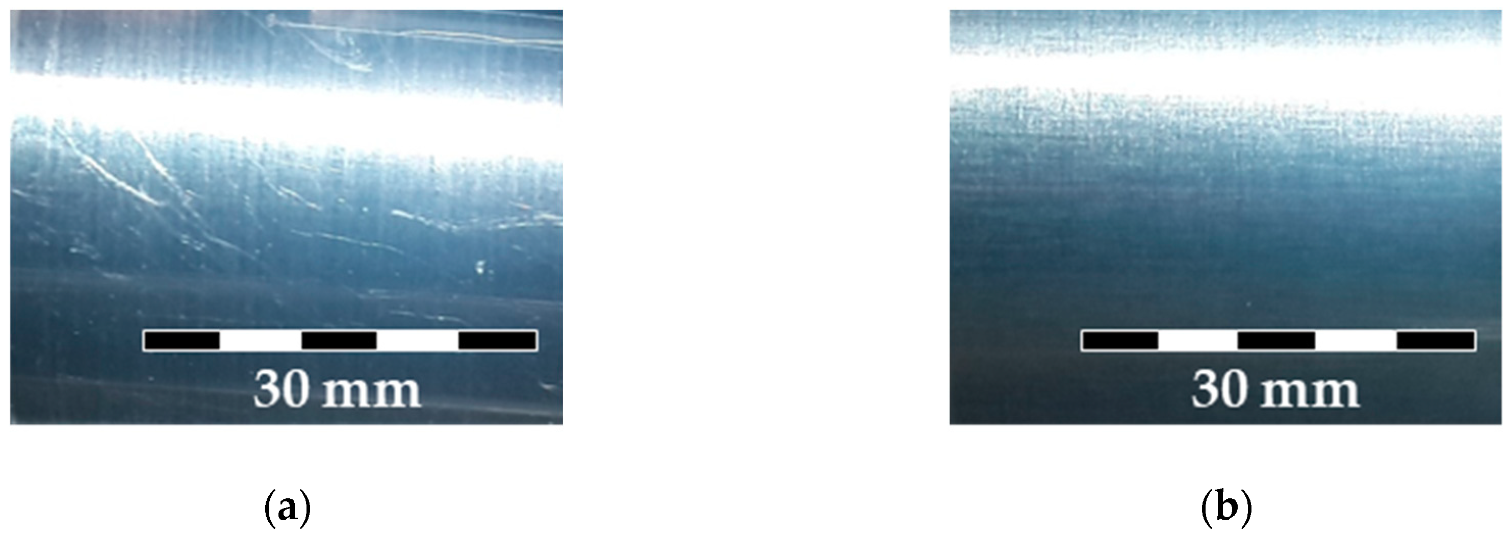
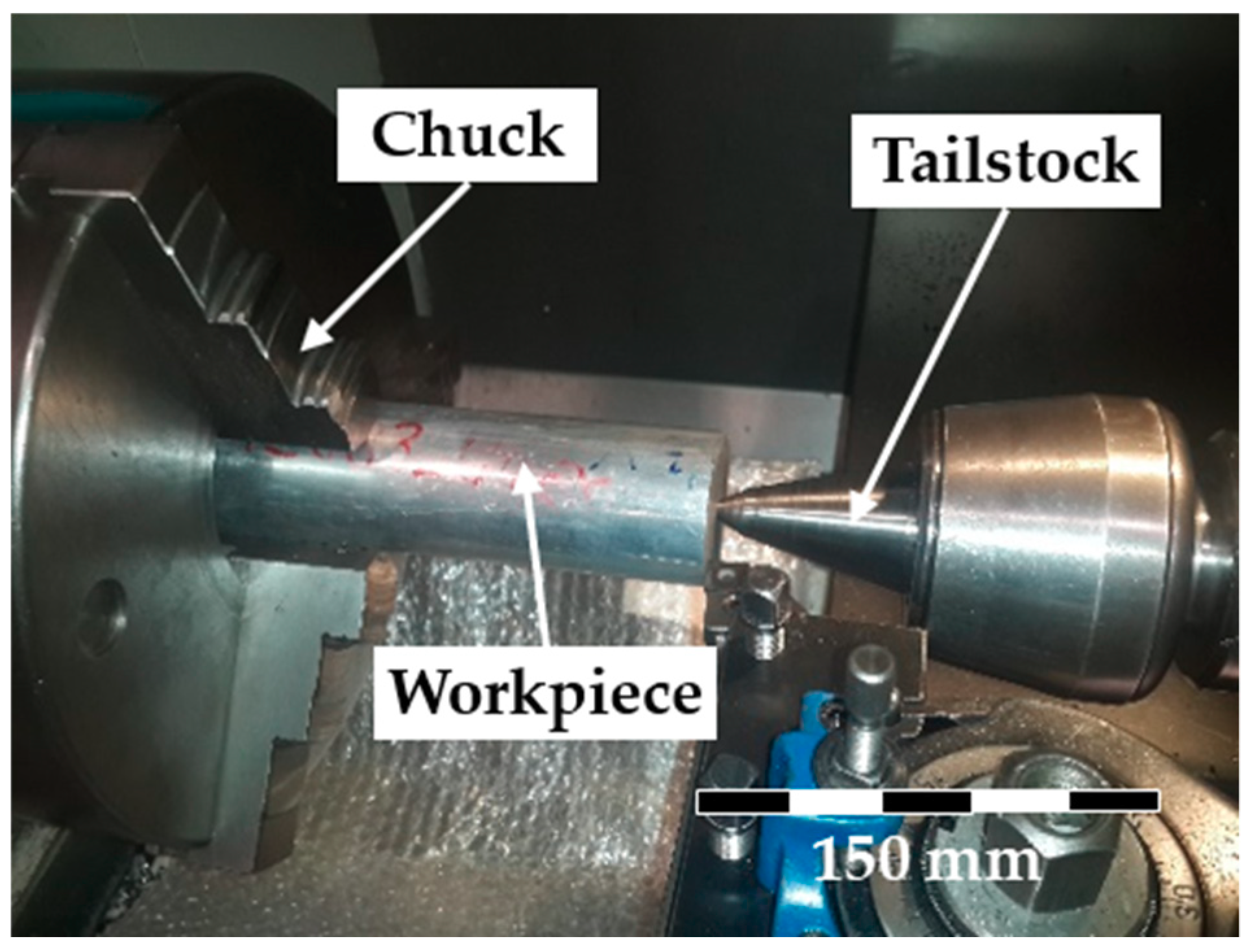
4. Experimental Turning Validation Tests

Practical machining tests were conducted to compare the performance of the tool-insert with its original geometry (no chip breaker) and with the one including the chip breaker. The test consisted in the longitudinal turning of an aluminum 6082 workpiece with the following cutting conditions: Ap = 1.0 mm, f = 0.10 mm and a Vc = 100 m/min, see Figure 11.
A profilometer Mitutoyo SJ-201P, Kawasaki, Kanagawa, Japan, was used to assess the finishing and also photos of the chips generated were taken.
Figure 12 shows the generated chips with and without a chip breaker. In particular, Figure 12a,c presents the chips that are the result of not using the chip breaker. Clearly, the chips generated were not curled and wrapped themselves around the workpiece. However, as can be seen in Figure 12b,d, with an insert including the chip breaker, the result was the generation of curly chips. Although these chips did not spontaneously break, they were curled and did evacuate from the newly machined surface and rake face of the insert in a controlled manner similar to that predicted by the simulation. This did help maintain a high-quality machined surface and did not increase the stresses on the cutting insert. These tests clearly confirmed that the insert with the chip breaker did generate curled chips, removing them from the cutting zone; and they also confirmed the fitness of the design of the chip breaker.
The roughness of the machined surfaces produced by both inserts were measured over two areas, close to the beginning and close to the end of the cutting path. For each area, five spot measurements were taken along a line parallel to the center line of the workpiece and the mean value was determined. The roughness, Ra, for the turning test using no chip breaker was 0.74 µm close to the beginning and 1.61 µm close to the end of the cutting path. The increase in Ra from 0.74 µm to 1.61 µm is attributed the presence of the uncurled chips, see Figure 12a,c. Close to the beginning, the chips can be seen to have moved away, at least partially, from the newly machined workpiece but as more chips are generated, their path is uncontrolled and they tend to clog the cutting zone and wrap around the workpiece, scratching the newly machined surface and lowering surface quality, see Figure 12a and Figure 13a. However, when conducting the turning test with a tool including a chip breaker, the Ra was 0.51 µm close to the beginning and 0.56 µm close to the end of the cutting path. Here the curling of the chips generated contributed to preserve high-quality finishing by ensuring the chips were evacuated from the working zone in a controlled manner; see Figure 13b.
This difference in generated roughness close to the beginning of the cutting path between the turning test using no chip breaker (Ra = 0.74 µm) and the test carried out using insert with chip breaker (Ra = 0.51 µm) can be attributed to the fact that the rake angle is bigger for the insert with chip breaker. Thus, the insert is sharper and the cut is smoother, reducing the built-up-edge (BUE).
Figure 14a,b show how the BUE was much pronounced in the tool without chip breaker when compared with the insert with chip breaker. Besides, the scratches can be seen in the insert as well. While the insert without chip breaker showed noticeable scratches, the one with chip breaker showed only minor scratches.

5. Conclusions

This study used a systematic approach to develop tailored, original chip breakers in polycrystalline diamond inserts, to assist the removal of chips generated under specific cutting conditions. FE analysis was utilized to create a 3D geometric design for a suitable chip breaker. Then, the 3D geometry was produced by the ablation of sequential layers of ablated material in the PCD insert using laser parameters optimized via initial experimental trials. Finally, real turning tests were conducted to compare the behavior of inserts with and without a chip breaker, with regard to chip formation and chips evacuation and, thus, to assess the reliability and efficiency of the chip breaker. The outcomes, in reference to the surface finishing and curly chip formation proved a clear and distinct improvement with the addition of the chip breaker.
Specific conclusions are as follows:
  • It was confirmed that the important geometric parameters defining the shape of the chip breaker are as follows: Rake angle, α; land width, a; tool-chip contact length, L; and radius of curvature, R.
  • Higher rake angles led to lower cutting forces, but that as stress in the tool edge increased, the tool became weaker.
  • It was found that a rake angle of 17° produced chips associated with a relatively low cutting force, while keeping sufficient tool strength to endure machining stresses without premature failure.
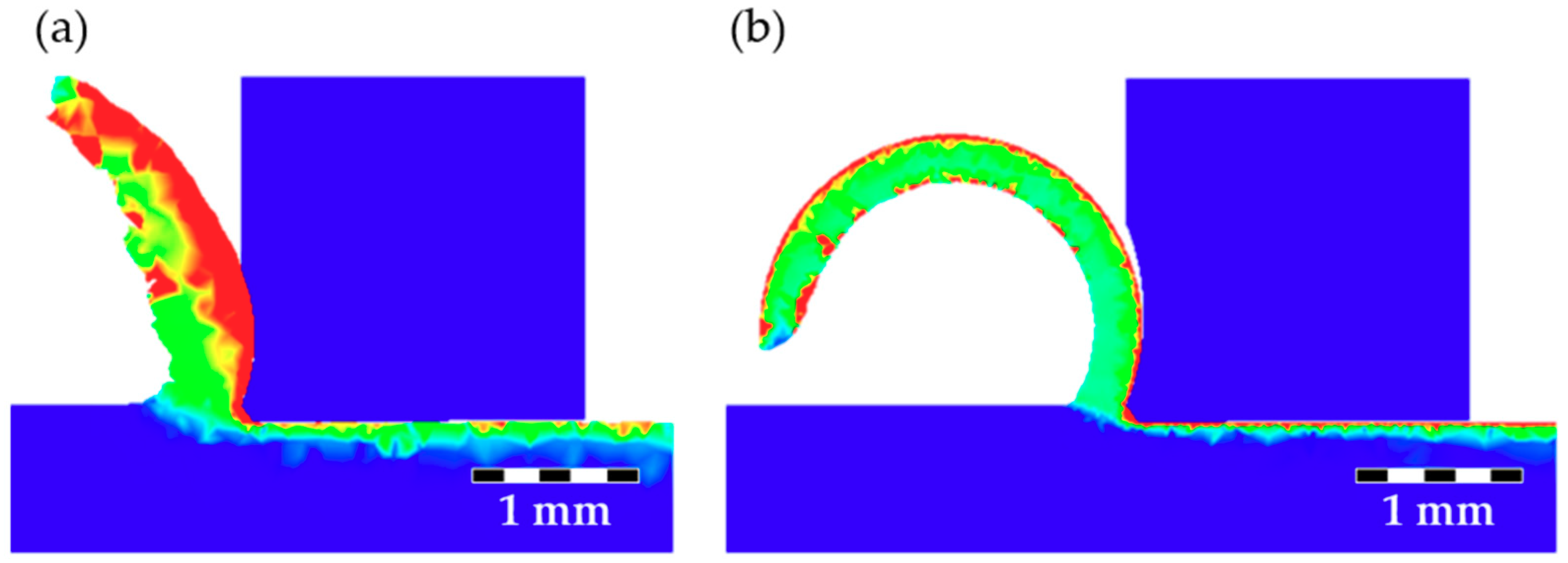
  • Optimum curling was found to take place with a land width being equal to half the feed rate.
  • For small chip breaker radius of curvature, (e.g., 1.0 mm) the chips were prone to getting clogged, leading to a dramatic increase of cutting efforts. A 1.4 mm radius of curvature for the chip breaker gave the best solution.
  • The results showed that a nano-second pulsed laser can be properly used to manufacture chip breakers.
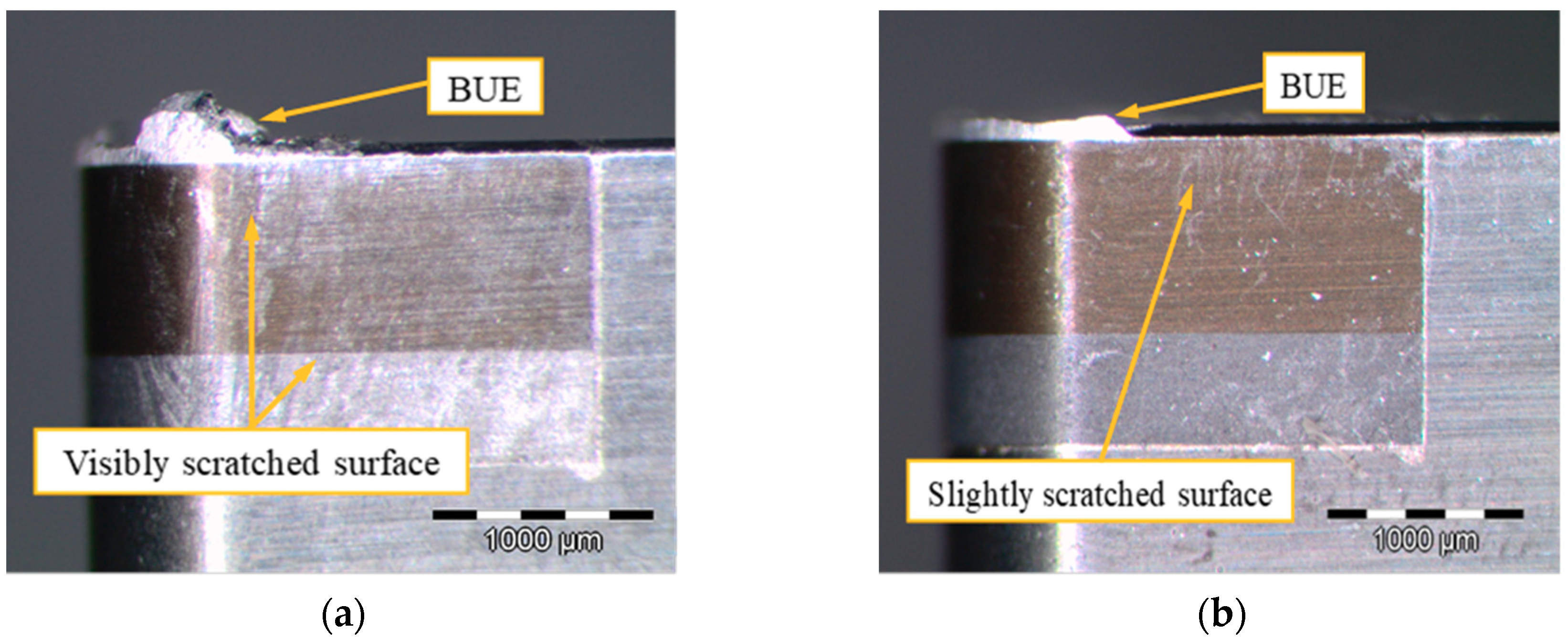
  • The insert that included the chip breaker was demonstrated to provide a curled chip formation, and reduced surface roughness significantly as well. This confirmed that the new tool-insert with a chip breaker is an effective solution, that the FE modelling is useful for the design stage, and that a nano-second laser is suitable for laser ablation.

Author Contributions

Conceptualization, I.C., J.A.S. and A.E.; data curation, I.C. and J.A.S.; formal analysis, I.C., J.A.S. and A.E.; funding acquisition, I.C. and J.A.S.; investigation, A.E., I.C. and J.A.S.; methodology, I.C., J.A.S. and A.E.; project administration, I.C. and J.A.S.; resources, I.C. and J.A.S.; software, I.C., J.A.S. and A.E.; supervision, A.E.; validation, A.E., I.C. and J.A.S.; visualization, A.E. and I.C., J.A.S.; writing—original draft, I.C., J.A.S. and A.E.; writing—review and editing, A.E.

Funding

This work was supported by the Department of Economic Development and Competitiveness of the Basque Government under HAZITEK program and by the budget of the European Regional Development Fund (ERDF) (grant number ZL-2017/00092).

Acknowledgments

The authors thank the support of Zubiola. Also, the authors gratefully acknowledge Jon Etxarri from Tekniker for his technical assistance.

Conflicts of Interest

The authors declare that there are no conflicts of interest.

References

  1. Polvorosa, R.; Suárez, A.; López de Lacalle, L.N.; Cerrillo, I.; Wretland, A.; Veiga, F. Tool wear on nickel alloys with different coolant pressures: Comparison of Alloy 718 and Waspaloy. J. Manuf. Process. 2017, 26, 44–56. [Google Scholar] [CrossRef]
  2. Alagan, N.; Zeman, P.; Hoier, P.; Tomas Beno, T.; Klement, U. Investigation of micro-textured cutting tools used for face turning of alloy 718 with high-pressure cooling. J. Manuf. Process. 2019, 37, 606–616. [Google Scholar] [CrossRef]
  3. Suárez, A.; Veiga, F.; López de Lacalle, L.N.; Polvorosa, R.; Wretland, A. An investigation of cutting forces and tool wear in turning of Haynes 282. J. Manuf. Process. 2019, 37, 529–540. [Google Scholar] [CrossRef]
  4. Goiogana, M.; Elkaseer, A. Self-Flushing in EDM Drilling of Ti6Al4V Using Rotating Shaped Electrodes. Materials 2019, 12, 989. [Google Scholar] [CrossRef] [PubMed]
  5. Kaya, E.; Akyüz, B. Effects of cutting parameters on machinability characteristics of Ni-based superalloys: A review. Open Eng. 2017, 7, 330–342. [Google Scholar] [CrossRef]
  6. Fan, Y.; Wang, T.; Hao, Z.; Liu, X.; Gao, S.; Li, R. Surface residual stress in high speed cutting of superalloy Inconel718 based on multiscale simulation. J. Manuf. Process. 2018, 31, 480–493. [Google Scholar] [CrossRef]
  7. Behera, B.; Alemayehu, H.; Ghosh, S.; Rao, P. A comparative study of recent lubri-coolant strategies for turning of Ni-based superalloy. J. Manuf. Process. 2017, 30, 541–552. [Google Scholar] [CrossRef]
  8. Li, G.; Yi, S.; Sun, S.; Ding, S. Wear mechanisms and performance of abrasively ground polycrystalline diamond tools of different diamond grains in machining titanium alloy. J. Manuf. Process. 2017, 29, 320–331. [Google Scholar] [CrossRef]
  9. Haddad, F.; Lescalier, C.; Desaigues, J.-E.; Bomont-Arzur, A.; Bomont, O. Metallurgical Analysis of Chip Forming Process when Machining High Strength Bainitic Steels. J. Manuf. Mater. Process. 2019, 3, 10. [Google Scholar] [CrossRef]
  10. Yılmaz, B.; Karabulut, Ş.; Güllü, A. Performance analysis of new external chip breaker for efficient machining of Inconel 718 and optimization of the cutting parameters. J. Manuf. Process. 2018, 32, 553–563. [Google Scholar] [CrossRef]
  11. Słodki, B.; Zębala, W.; Struzikiewicz, G. Turning titanium alloy, grade 5 ELI, with the implementation of high pressure coolant. Materials 2019, 12, 768. [Google Scholar] [CrossRef] [PubMed]
  12. Elsanabary, S.; Elkaseer, A.; Abd-Rabbo, S.; AbdElsalam, M.; Abdou, S. Modelling and experimental validation of surface roughness in precision turning of dual-phase materials considering process uncertainties. Int. J. Interact. Des. Manuf. 2019, 13, 59–74. [Google Scholar] [CrossRef]
  13. Gao, H.; Liu, X.; Chen, Z. Cutting Performance and Wear/Damage Characteristics of PCBN Tool in Hard Milling. Appl. Sci. 2019, 9, 772. [Google Scholar] [CrossRef]
  14. Lotfi, M.; Akhavan Farid, A.; Soleimanimehr, H. The effect of chip breaker geometry on chip shape, bending moment, and cutting force: FE analysis and experimental study. Int. J. Adv. Manuf. Technol. 2015, 78, 917–925. [Google Scholar] [CrossRef]
  15. Chu, N.; Nguyen, D.; Ngo, N.; Nguyen, V.; Tran, M.; Vu, N.; Ngo, Q.; Tran, T. A New Approach to Modelling the Drilling Torque in Conventional and Ultrasonic Assisted Deep-Hole Drilling Processes. Appl. Sci. 2018, 8, 2600. [Google Scholar] [CrossRef]
  16. Shamoto, E.; Aoki, T.; Sencer, B.; Suzuki, N.; Hino, R.; Koide, T. Control of chip flow with guide grooves for continuous chip disposal and chip-pulling turning. CIRP Ann. 2011, 60, 125–128. [Google Scholar] [CrossRef]
  17. Miyake, A.; Kitakaze, A.; Katoh, S.; Muramatsu, M.; Noguchi, K.; Sannomiya, K.; Nakaya, T.; Sasahara, H. Chip control in turning with synchronization of spindle rotation and feed motion vibration. Precis. Eng. 2018, 53, 38–45. [Google Scholar] [CrossRef]
  18. Buchkremer, S.; Klocke, F.; Veselovac, D. 3D FEM simulation of chip breakage in metal cutting. Int. J. Adv. Manuf. Technol. 2016, 82, 645–661. [Google Scholar] [CrossRef]
  19. Pereira, O.; Rodríguez, A.; Fernández-Abia, A.I.; Barreiro, J.; López de Lacalle, L.N. Cryogenic and minimum quantity lubrication for an eco-efficiency turning of AISI 304. J. Clean. Prod. 2016, 139, 440–449. [Google Scholar] [CrossRef]
  20. Pereira, O.; Rodríguez, A.; Barreiro, J.; Fernández-Abia, A.I.; de Lacalle, L.N.L. Nozzle design for combined use of MQL and cryogenic gas in machining. Int. J. Precis. Eng. Manuf. 2017, 4, 87–95. [Google Scholar] [CrossRef]
  21. Kaynak, Y.; Gharibi, A. Progressive Tool Wear in Cryogenic Machining: The Effect of Liquid Nitrogen and Carbon Dioxide. J. Manuf. Mater. Process. 2018, 2, 31. [Google Scholar] [CrossRef]
  22. Klocke, F.; Lortz, W.; Trauth, D. Analysis of the dynamic chip formation process in turning. Int. J. Mech. Sci. 2018, 135, 313–324. [Google Scholar] [CrossRef]
  23. Rahimzadeh Berenji, K.; Karagüzel, U.; Özlü, E.; Budak, E. Effects of turn-milling conditions on chip formation and surface finish. CIRP Ann. 2019, 68, 113–116. [Google Scholar] [CrossRef]
  24. Li, B.; Zhang, S.; Zhang, Q.; Li, L. Simulated and experimental analysis on serrated chip formation for hard milling process. J. Manuf. Process. 2019, 44, 337–348. [Google Scholar] [CrossRef]
  25. Lotfi, M.; Farid, A.A.; Soleimanimehr, H. A new hybrid model based on the radius ratio for prediction of effective cutting limit of chip breakers. Proc. Inst. Mech. Eng. Part B J. Eng. Manuf. 2016, 230, 1417–1427. [Google Scholar] [CrossRef]
  26. Elkaseer, A.; Lambarri, J.; Sarasua, J.A.; Cascón, I. On the development of a chip breaker in a metal-matrix polycrystalline diamond insert: Finite element based design with ns-laser ablation and machining verification. J. Micro Nano Manuf. 2017, 5, 031007. [Google Scholar] [CrossRef]
  27. Soares, R.B.; de Jesus, A.M.P.; Neto, R.J.L.; Rosa, P.A.R.; Machado, M.; Reis, A. Machinability of an Aluminium Cast Alloy Using PCD Tools for Turning. In Materials Design and Applications; Silva, L., Ed.; Springer: Berlin/Heidelberg, Germany, 2017; pp. 329–346. [Google Scholar]
  28. Diamond, L. Products, PCD and CBN Tools, Inserts with Chipbreaker. Available online: http://www.lach-diamond.com/LDI/products/pcd-and-cbn-tools/turning---drilling---milling/inserts-with-chipbreaker (accessed on 7 June 2019).
  29. Carbide, M. Technical Information about PCD Turning Inserts. Available online: http://www.mitsubishicarbide.net/contents/mhg/enuk/html/product/technical_information/grade/turning/pcd.html (accessed on 7 June 2019).
  30. Coromant, S. Chip Breaking in CNC Turning. 2016. Available online: https://www.cadem.com/single-post/cnc-turning-chip-breaking (accessed on 3 July 2019).
  31. Xiong, Y.; Wang, W.; Jiang, R.; Lin, K.; Shao, M. Mechanisms and FEM Simulation of Chip Formation in Orthogonal Cutting In-Situ TiB2/7050Al MMC. Materials 2018, 11, 606. [Google Scholar] [CrossRef]
  32. Elkaseer, A.; Abdelaziz, A.; Saber, M.; Nassef, A. FEM-Based Study of Precision Hard Turning of Stainless Steel 316L. Materials 2019, 12, 2522. [Google Scholar] [CrossRef]
  33. Gonzalo, O.; Quintana, I.; Etxarri, J. FEM Based Design of a Chip Breaker for the Machining with PCD Tools. Adv. Mater. Res. 2011, 223, 133–141. [Google Scholar] [CrossRef]
  34. Chen, D.C.; You, C.S.; Kao, S.H. Finite element analysis of chip breaker geometry in turning process. Adv. Mech. Eng. 2016, 8, 1687814016659823. [Google Scholar] [CrossRef]
  35. Gurbuz, H.; Kurt, A.; Seker, U. Investigation of the effects of different chip breaker forms on the cutting forces using artificial neural networks. Gazi Univ. J. Sci. 2012, 25, 803–814. [Google Scholar]
  36. Sreekala, P.; Visweswararao, K. A methodology for chip breaker design at low feed turning of alloy steel using finite element modelling methods. Int. J. Mech. Eng. Technol. 2012, 3, 263–273. [Google Scholar]
  37. Third Wave Systems. Third Wave AdvantEdge™. Available online: www.thirdwavesys.com/advantedge/ (accessed on 7 June 2019).
  38. Shokrani, A.; Newman, S.T. A New Cutting Tool Design for Cryogenic Machining of Ti–6Al–4V Titanium Alloy. Materials 2019, 12, 477. [Google Scholar] [CrossRef] [PubMed]
  39. Tsai, M.Y.; Chang, C.T.; Ho, J.K. The Machining of Hard Mold Steel by Ultrasonic Assisted End Milling. Appl. Sci. 2016, 6, 373. [Google Scholar] [CrossRef]
  40. Astakhov, V.P. Tribology of Metal Cutting; Elsevier: Amsterdam, The Netherlands, 2006. [Google Scholar]
  41. Eberle, G.; Wegener, K. Ablation study of WC and PCD composites using 10 picosecond and 1 nanosecond pulse durations at green and infrared wavelengths. In Proceedings of the 8th International Conference on Photonic Technologies, Physics Procedia, Fürth, Germany, 8–11 September 2014; Volume 56, pp. 951–962. [Google Scholar]
  42. Eberle, G.; Jefimovs, K.; Wegener, K. Characterisation of Thermal Influences After Laser Processing Polycrystalline Diamond Composites Using Long to Ultra-Short Pulse Durations. Precis. Eng. 2015, 39, 16–24. [Google Scholar] [CrossRef]
Figure 1. Chip breaking methods (a) breaks on its own; (b) breaks against the tool; (c) breaks against workpiece.
Applsci 09 04117 g001
Figure 2. Geometric parameters of the chip breaker: Land width (a), tool-chip contact length (L), rake angle (α), radius of curvature ® and groove width (W).
Applsci 09 04117 g002
Figure 3. A rhombic 80° turning insert: (a) The actual insert and (b) side view of the geometry of the chamfer. (Dimensions in mm).
Applsci 09 04117 g003
Figure 4. Result of chip curling simulations.
Applsci 09 04117 g004
Figure 5. Detail of the area close to the cutting edge for the selected design: α = 20°, a = 0.05 mm.
Applsci 09 04117 g005
Figure 6. Bending of the chip as a result of the radius of curvature with (a) R = 1 mm; (b) R = 1.4 mm.
Applsci 09 04117 g006
Figure 7. Chip breaker geometry result from the simulation study (a) cross-section in 2D (b) geometry in 3D [all dimensions as in mm].
Applsci 09 04117 g007
Figure 8. FE simulation result for the final chip breaker geometry.
Applsci 09 04117 g008
Figure 9. Ablated chip breaker in the polycrystalline diamond (PCD) insert.
Applsci 09 04117 g009
Figure 10. Measurement of the ablated chip breaker in the PCD insert.
Applsci 09 04117 g010
Figure 11. Turning trials: Set up for an aluminum workpiece.
Applsci 09 04117 g011
Figure 12. Generated chips (a) turning test using insert without a chip breaker with generated chips wrapped around the workpiece, (b) turning test with insert including chip breaker, where chips are evacuated, (c) straight chips as a result of turning test with original insert geometry, no chip breaker, and (d) curly chips as a result of turning test with insert including chip breaker.
Applsci 09 04117 g012
Figure 13. Machined surfaces produced by inserts: (a) Without chip breaker, where uncontrolled chips scratched the newly machined surface; (b) with chip breaker, where chips were properly removed from the cutting zone and good quality finishing is preserved.
Applsci 09 04117 g013
Figure 14. Inserts used in the machining trials (a) large built-up-edge (BUE) and noticeable scratches in the insert without chip breaker and (b) small BUE and minor scratches in the insert with chip breaker.
Applsci 09 04117 g014
Table 1. Cutting conditions.
Workpiece MaterialsAl 6082
Depth of cut (Ap)1 mm
Cutting Velocity (Vc)100 m/min
Feed rate (f)0.1 mm/rev
Table 2. Results of the simulation for rake angle (α) and land width (a).
α (°)a (mm)Cutting Force (N)Temperature (°C)Radius of Curvature of the Chip (mm)
100170.9185.26.5
100.05161.2179.35
100.1160.1171.92
100.15161.1175.02.25
200148.1172.94.75
200.05139.1160.21.45
200.1155.2169.01.88
200.15158.6174.92
300123.8159.12.65
300.05138.4161.91.55
300.1151.5172.01.75
300.15156.3178.25.5

