Featured Application
Automatic test equipment, Measurement instruments.
Abstract
In this paper, a digital-to-time converter (DTC) based on the three delay lines (3D) Vernier principle is proposed and implemented with field programmable gate arrays (FPGAs). Based on the 3D Vernier principle, the DTC is realized by three period approximate phase locked loops (PLLs). The theoretical fine resolution of the proposed DTC is improved by calculating the period difference two times. The achieved resolution of the proposed DTC is 203 fs realized with an Altera Stratix III FPGA chip, which is about tenfold higher than traditional FPGA-DTC implemented with the same series FPGAs. The worst absolute differential nonlinearity (DNL) and integral nonlinearity (INL) are verified smaller than 0.88 least significant bit (LSB) and 4.4 LSB, respectively. By optimized computation logic, there are only 448 adaptive look-up-tables (ALUTs), 237 registers and three phase locked loops (PLLs) utilized for circuit implementation. Experimental results prove that the proposed DTC features high resolution with low cost.
1. Introduction
A digital-to-time converter (DTC) is used to generate a time signal with a width that is proportional to the programmable input digital value. It has been widely used in the fields of automatic test equipment (ATE) or measurement instruments [1,2,3,4,5,6,7,8,9,10,11,12]. High resolution is the most critical consideration in DTC design, which means high precision and high performance of ATE and measurement instruments. In terms of implementing methods, the DTCs can be classified as application specific integrated circuit (ASIC) DTC [1,2,3,4,5,6,7,9] and field programmable gate arrays FPGA-DTC [6,8,11]. The resolution of ASIC-DTCs can be better than 1 ps, which is realized with the capacitor charging circuit. But the ASIC-DTCs are limited by small dynamic range, high cost and long development time. The DTCs also can be classified with absolute [1,2,3,4,5,6,7,12] or relative [8,9,10,11] time generation due to different operations. The absolute time generations have wide dynamic ranges but poor resolution performance. They are also sensitive to process, voltage and temperature (PVT) variations. On the contrary, the relative time generations have much finer resolution and are robust to PVT. However, the relative methods are hampered by path or element mismatches.
Since a digitally-implemented DTC is usually realized by logic gates or delay lines, FPGAs which inherently include logic gates and phase locked loops (PLLs) attract research interest on DTC implementation. Moreover, the lower cost and shorter time-to-market also motivate the development of FPGA-DTCs. Nowadays, FPGA-DTCs which are realized by phase-shifting can obtain about 8 ps resolution [6,9]. To increase the resolution, a DTC based on the Vernier principle was proposed in [11]. It achieved a 1.58 ps resolution using two integrated PLLs with Altera Stratix-III FPGA. Similarly, the quantified phase shift resolution (QPSR) DTC proposed in [8] obtained a 3.93 ps resolution with Xilinx Virtex-6 FPGA. However, the high resolution of these methods is achieved with advanced FPGAs. The Vernier DTC and QPSR DTC realized with Xilinx Virtex-5 FPGA only obtained 35.27 ps and 27.1 ps resolution, respectively. Therefore, a high resolution and low-cost FPGA-DTC is not only valuable for practical applications, but also very challenging for researchers.
In this paper, a novel DTC realized with the three delay lines Vernier principle (3D Vernier DTC) is proposed and evaluated. The resolution of the proposed DTC is 203 fs implemented with Altera Stratix-III FPGAs. The theoretical resolution of 3D Vernier DTC can be tenfold higher than traditional Vernier DTCs and QPSR DTCs implemented with the same FPGAs. Moreover, the DTC obtains 13.5 ps resolution even with the cheapest Altera Cyclone-IV E FPGAs. The high-resolution performance of the proposed DTC benefits from the high, medium and slow Vernier delay line constructed by PLLs, which ensures fine resolution and robustness to PVT variation.
2. Operation Principle of the Proposed DTC
2.1. Principle of Vernier DTC
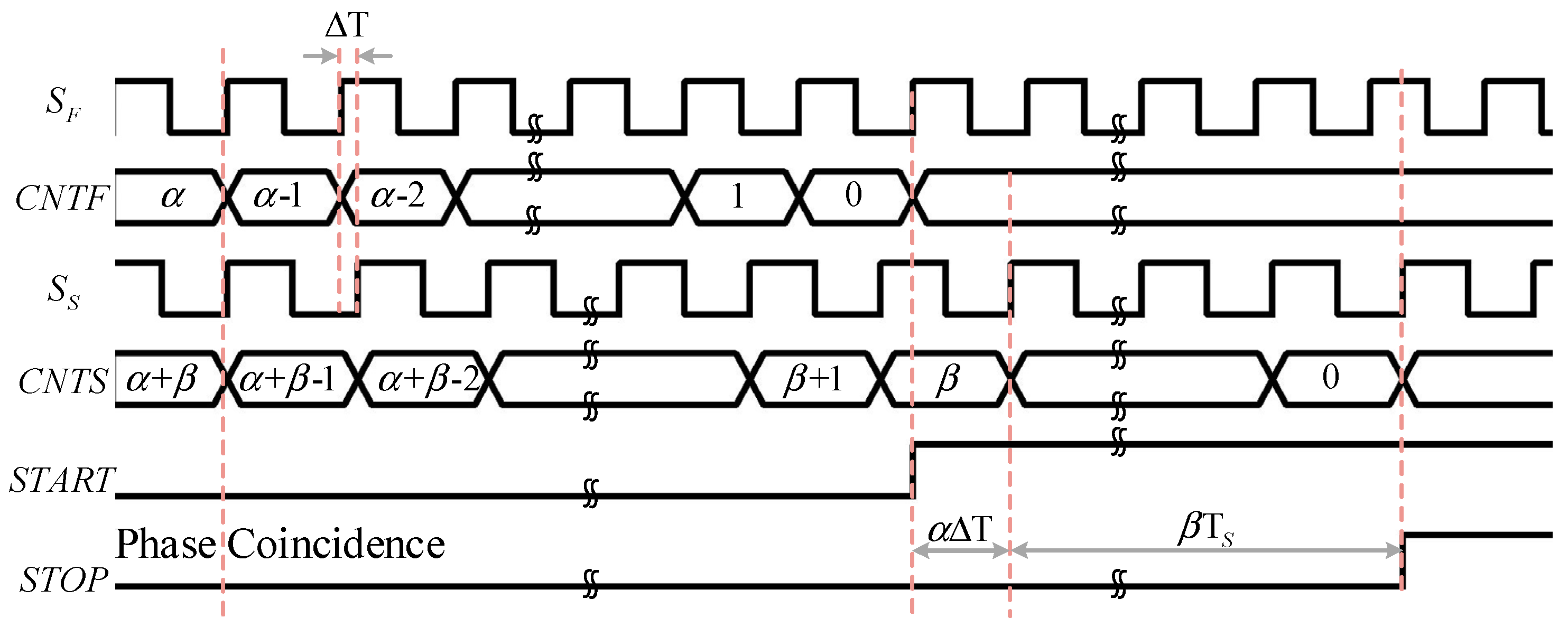
The Vernier principle has been widely used for time-to-digital converter design in previous researches [13]. It is firstly introduced to FPGA-DTC in [11]. The typical timing diagram of Vernier FPGA-DTC is shown in Figure 1. SF and SS represent two periodic signals, with frequencies quite close to each other. Fast counter (CNTF) and slow counter (CNTS) are the down counters clocked by SF and SS. After the coincidence of the rising edge between SF and SS, the counters CNTF and CNTS start to count α and β cycles, respectively. α and β are the fine and coarse counting values of Vernier DTC. The generated time width between START and STOP signals can be expressed as:
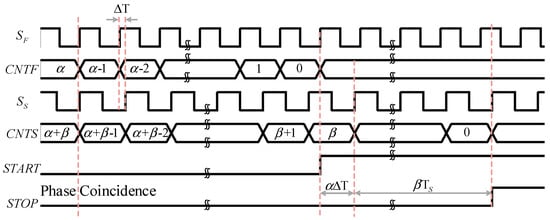
Figure 1.
Timing diagram of Vernier digital-to-time converter (DTC).
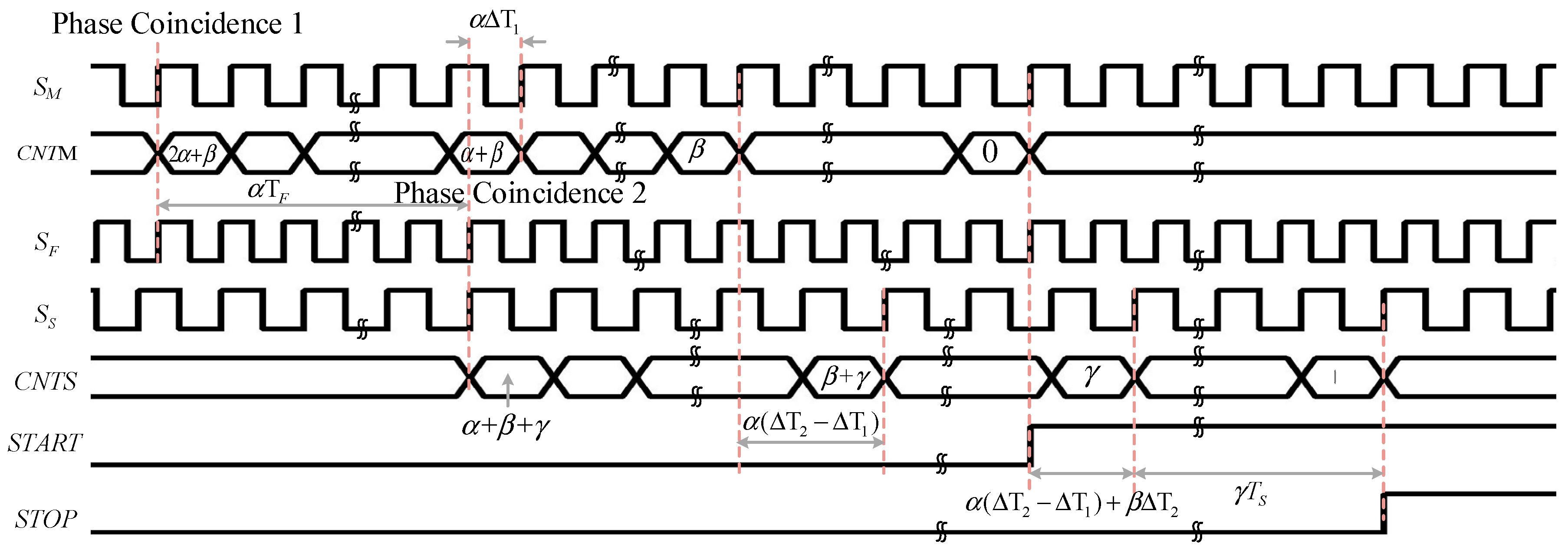
The resolution of Vernier DTC is determined by the period difference between SF and SS. Therefore, the frequency resolution of PLLs on FPGAs limited the performance of Vernier FPGA-DTC. For instance, 8TS = 9TF, thus the resolution of this DTC is (1/9)TS, as shown in Figure 1. Now we suppose that we can get three signals which have approximate periodical signals, SF (fast), SM (medium) and SS (slow). The relationship of their period is 8TS = 9TM = 10TF, as shown in Figure 2. The time difference ∆T1, ∆T2 and ∆T are defined as:
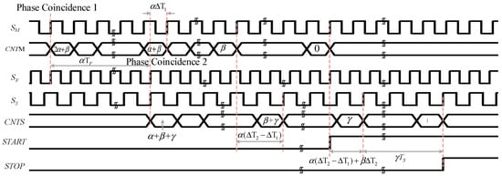
Figure 2.
Timing diagram of the proposed three delay lines (3D) Vernier DTC.
For a common case, (n − 1)TS = nTM = (n + 1)TF, where n is a positive integer. In this case, the resolution of DTC is 2TS/(n(n + 1)). It is much higher than two delay lines Vernier DTC with the same n (n >> 2). The detailed timing diagram of 3D Vernier DTC is shown in Figure 2. The down counter CNTM starts to count 2α + β cycles after the phase coincidence (Phase Coincidence 1) of SF and SM. The phase of slow clock SS coherent with SF after αTF (Phase Coincidence 2). At this moment, the counter CNTS starts to count α + β + γ cycles. The output time width becomes:
For the DTC output continuously varying in step size ∆T, ∆T2 should be integer multiples of ∆T. It means that (n + 1)/2 should be a positive integer. In other words, n should be an odd positive integer number. To generate a given time width X∆T which is equal to , we have:
where denotes the largest integer number less than or equal to x. Usually, the odd integer number n is designated as several decades to get a much higher resolution. The generation time from changing input value to STOP enable can be expressed as:
2.2. Circuit Description of 3D Vernier DTC
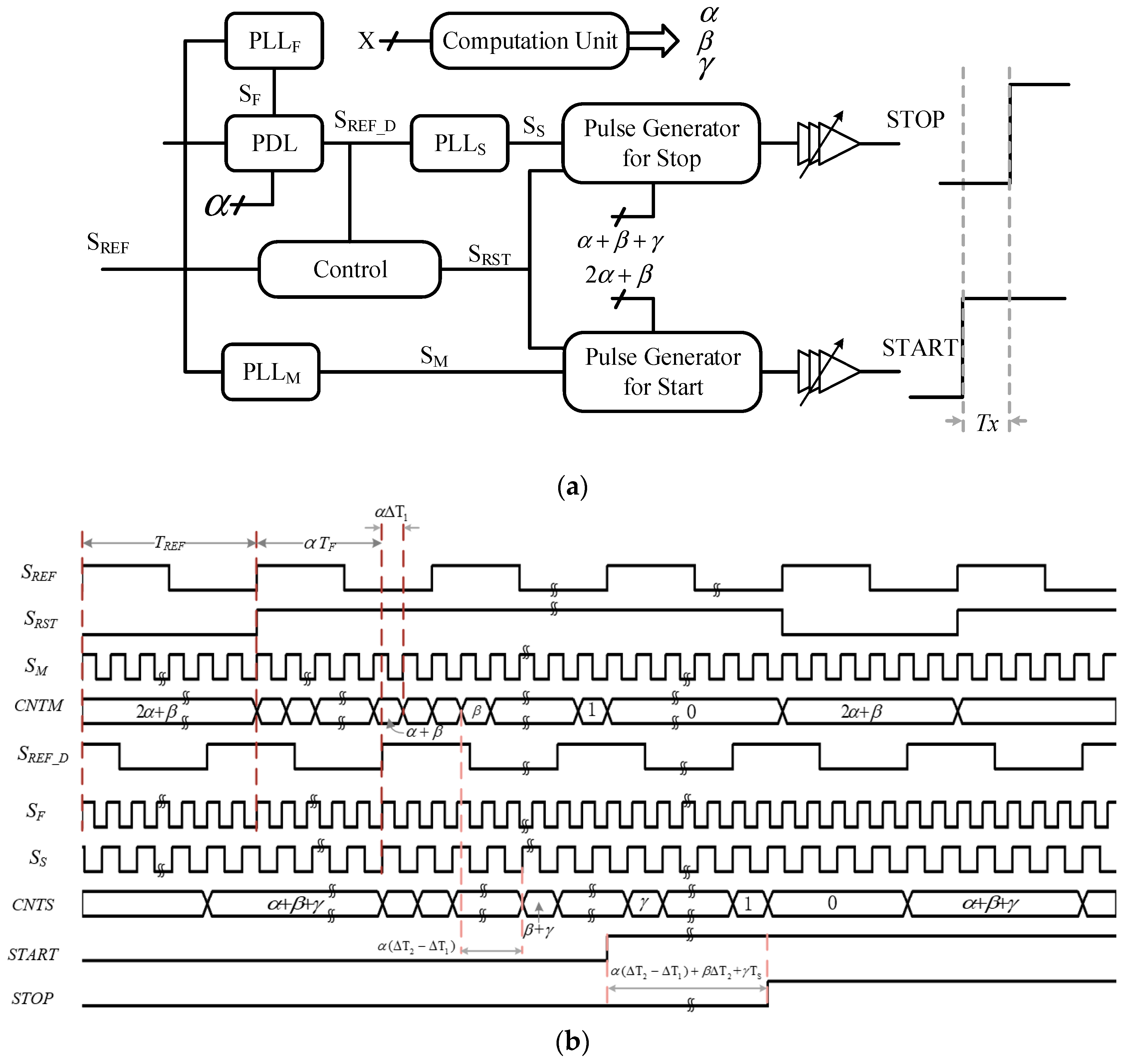
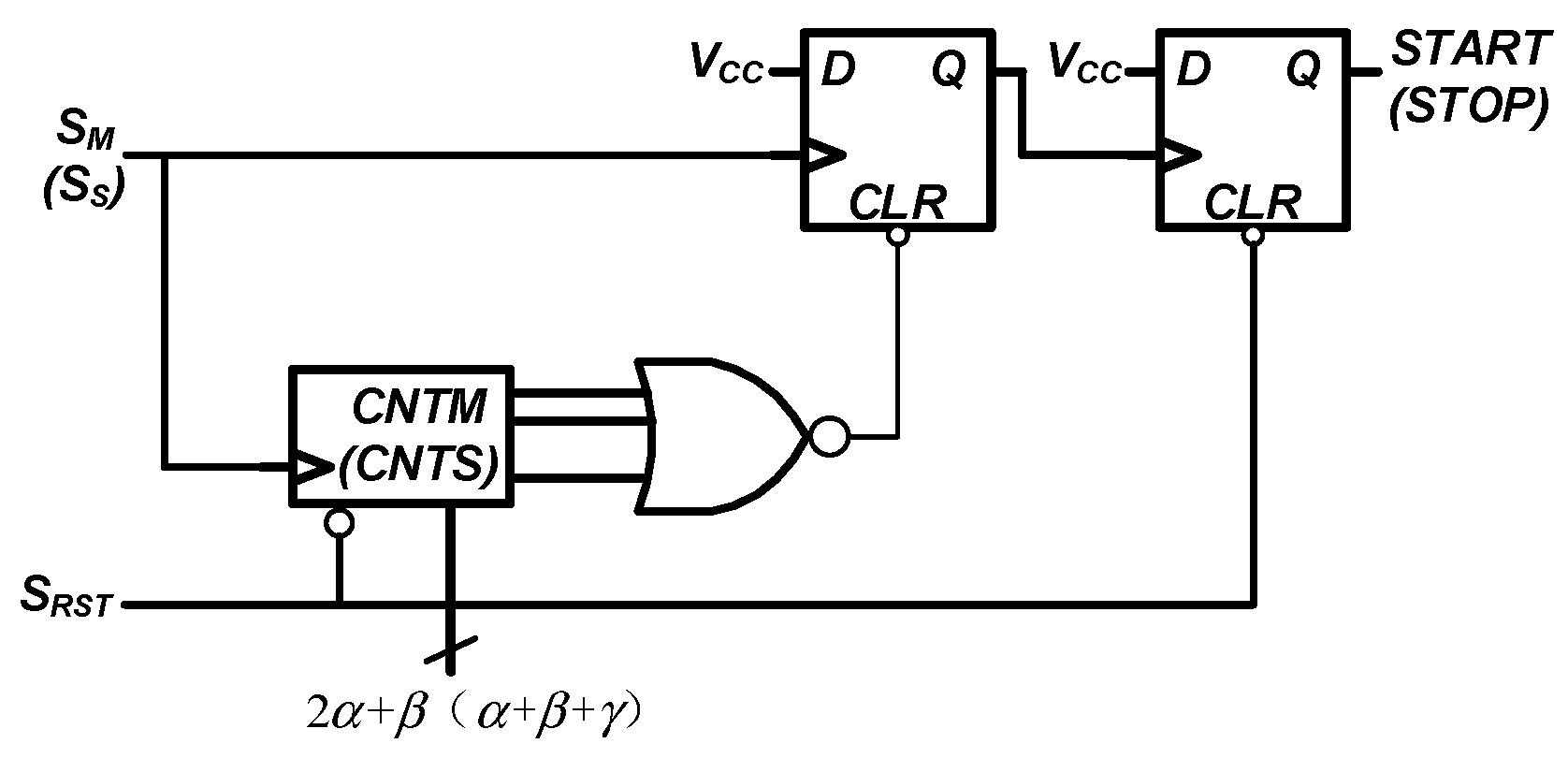
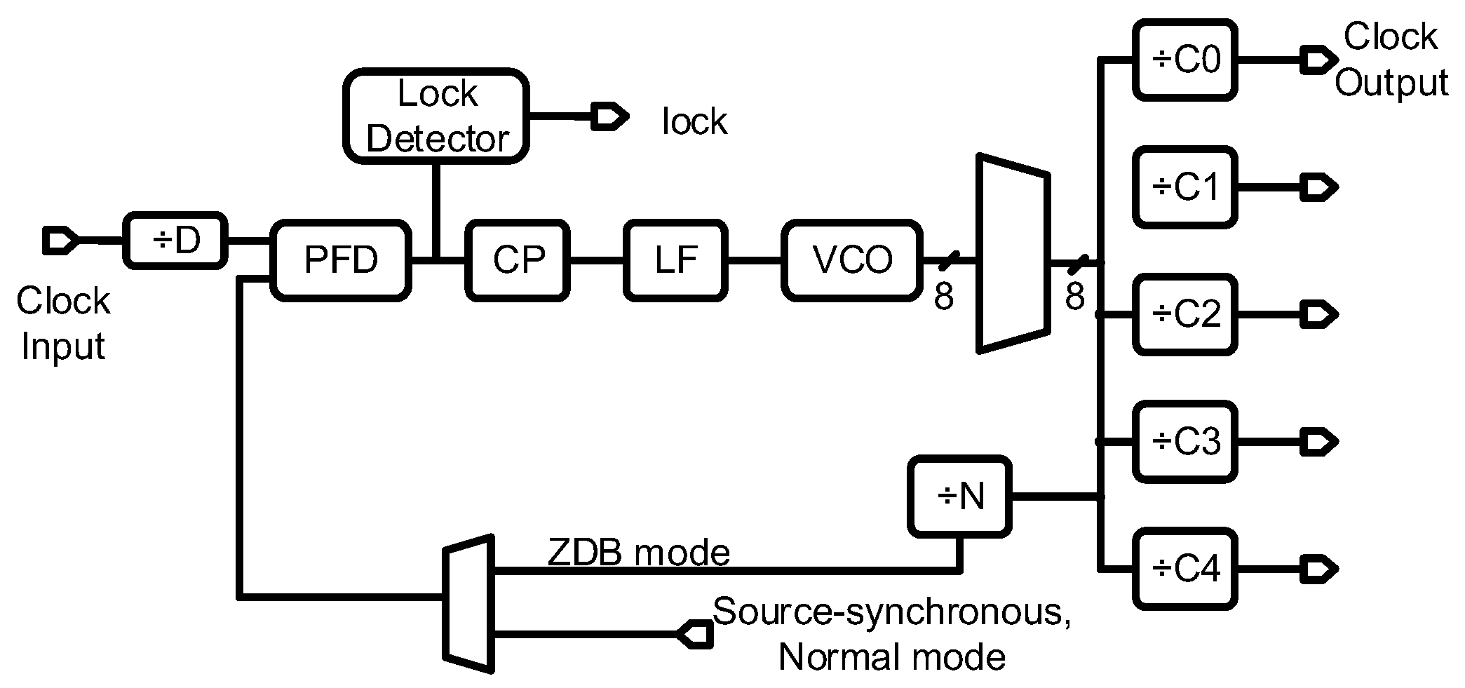
The simplified block diagram and timing diagram of the proposed 3D Vernier DTC are shown in Figure 3. Three PLLs (PLLF, PLLM and PLLS) with approximate periods are utilized to generate the time difference ∆T1, ∆T2 and ∆T. The high resolution is obtained by employing the Vernier principle two times. The main challenge in the circuit design of the proposed DTC is aligning the rising edge of SF, SM and SS at the correct time. The accuracy of phase coincidence measurement should be better than 1 least significant bit (LSB) of DTC to distinguish the correct phase coincidence moment. Since the PLLs can realign the rising edges of SF and SM to SREF, each rising edge of SREF indicates one phase coincidence of SF and SM. Even if there is an error between the two rising edges, it is a constant value decided by the PLLs. Similarly, the rising edge of SS can be synchronized to SREF_D. SREF_D is generated from SREF by the programmable delay line (PDL), which is realized with D-type flip-flop (DFF) as shown in Figure 4. Because of the DFFs identity among the whole programmable delay line, they have the same synchronization deviation with different input value. Since the step size of this PDL is TF, SREF_D is a delay of SREF with αTF. Therefore, the rising edge of SREF_D is synchronized to SF. The rising edge of SREF_D indicates the phase coincidence of SF and SS, as shown in Figure 3b. The reset signal SRST would periodically reset the counter in the pulse generators. The counters in the pulse generator are reloaded and enabled by SRST. Thus, the duty cycle of output signals START and STOP would be 50%. The clock of pulse generators are provided by PLLM and PLLS. The preset value 2α + β and α + β + γ of pulse generators are generated from the computation unit. Figure 5 shows the schematic diagram of the output pulse generator. After CNTM or CNTS count to 0, the output of the NOR gate will be pulled high. Then the output of the two DFFs will be flipped at the next rising edge of SM or SS.

Figure 3.
Simplified block diagram and timing diagram of proposed DTC: (a) Block diagram, (b) Timing diagram.
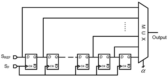
Figure 4.
Schematic diagram of a programmable delay line (PDL).
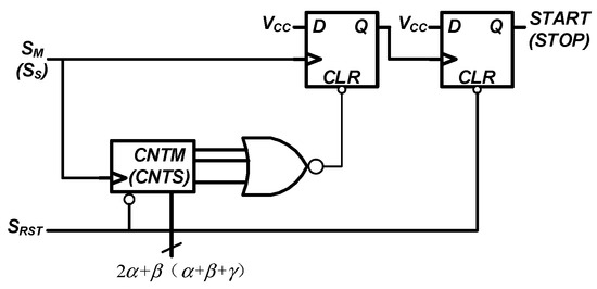
Figure 5.
Schematic diagram of a pulse generator.
Since the logic gates in PDL are synchronized to SF and the logic gates in pulse generators are synchronized to SM or SS, the latency mismatch between these signals would cause time error on DTC output. Thus, we insert some delay cells which consist of inverters in the output path of START or STOP signals to compensate for the timing mismatch introduced by the different transmission path. When the proposed DTC is implemented with Stratix III FPGA, the delay in the start path is a little larger than it is in the stop path. The residual different route delays can be compensated for by adding a constant value on the input value X. The Altera Quartus II software can specify the arrival times of different signals at the expense of considerable increases of compilation time and area by enabling netlist optimizations and physical synthesis options [14,15]. Moreover, the arriving time of SF, SM, SS, STRAT and STOP signals can be specified by set_input_delay, set_max_dealy and set_min_dealy constraints by users. Moreover, the proposed DTC is insensitive to PVT variation because the output signals are synchronized to PLLs’ outputs.
For a given time width X∆T, the corresponding value of α, β and γ can be derived from Equation (6). However, it consumes a lot of logic gates and power to process division and remainder operation in the digital circuit design. For the sacrifice of some design flexibility, we can design the computation unit just with some adders in a binary system, as shown in Equation (8).
where q denotes the integer quotient of a and b, bx denotes the nth fractional place of 1/b in binary. For a given b, the bx is determined as 0 or 1. For example, when b equal to 31 and x is an integral multiple of five, bx = 1, otherwise, bx = 0. To reduce the design complexity and the cost of the computation unit, the n in Equations (5) and (6) is recommended to be selected as 2M − 1. Thus, the remainder can be calculated as:
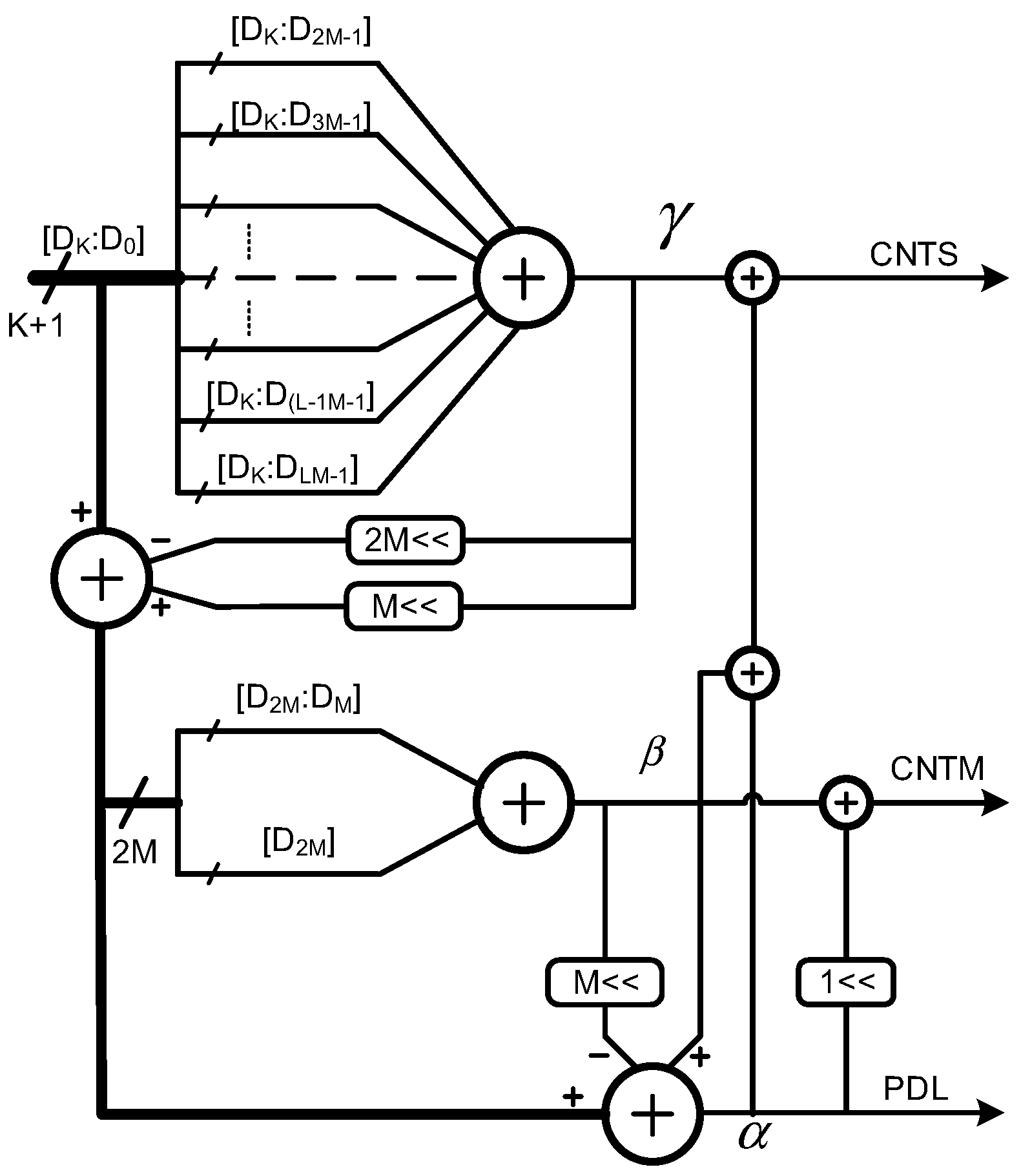
In this case, all of the computation units can be realized by very few adders, as shown in Figure 6. The maximum number of α needs to be (n + 1)/2 − 1, which is the ratio of medium and fine resolution in Equation (5). The maximum number of β and γ is n − 1 and 2K − 2M + 1, respectively. Therefore, the number of delay stages in PDL is designed as 2M, the input bits width of CNTM is 2M and the input bits width of CNTS is K − 2M + 2 for a K bits DTC.

Figure 6.
Computation unit for counters and PDL in the proposed DTC.
3. Experimental Results
With the development of complementary metal-oxide semiconductor (CMOS) technology, most digital circuits can be implemented with FPGA for shortening development time. Furthermore, most FPGAs inherently integrated several high performance PLLs in the chips. It is easy to get an accurate delay time by these PLLs, which can be utilized as PLLF, PLLM and PLLS. In this paper, we adopt Altera Cyclone IV FPGA for function verification and Altera Stratix III FPGA for performance evaluation.
3.1. Implementation with Cyclone IV E FPGA
Altera Cyclone IV E series FPGAs, which were issued in 2009, have been widely used in many research fields for their very low cost and low power consumption. The Cyclone IV E FPGA embed four PLLs which can be used to generate periodical signals in conventional and proposed Vernier DTCs, since the resolution of both conventional and proposed Vernier DTCs is determined by the performance of PLLs. The block diagram of the PLL in Cyclone IV E FPGA is depicted in Figure 7 [16]. PLL parameters are shown in Table 1 [16,17].

Figure 7.
Block diagram of phase locked loop (PLL) in Cyclone IV E and Stratix III field programmable gate arrays (FPGAs) [16].

Table 1.
PLL parameters of adopted FPGAs [16,17].
According to the measurement, the maximum working frequency of our design implemented with Cyclone IV E series FPGAs is limited to 200 MHz. To pursue a higher working frequency, it needs more complex logic implementation and optimized place and route at the expenses of complexity and reliability. For Vernier FPGA-DTCs, the rising edge of the reference clock is set as the phase coincidence of two periodical signals. Thus, the output signals of two PLLs should be integer times of reference clock. Moreover, the input frequency range of PLLs is 5–474 MHz. To ensure the PLL outputs have the same phase at every rising edge of reference clock, the PLLs should work at integer-N mode. Therefore, the finest frequency resolution is 5 MHz and the highest time resolution of traditional Vernier DTC with 200 MHz working frequency can be obtained as:
Besides, the resolution of conventional Vernier DTC will be much worse with lower working frequency, since the minimum reference frequency of Cyclone IV E and Stratix III is 5 MHz, and the input frequency from crystal frequency is 50 MHz. Thus, D is chosen as 10 to obtain the minimum frequency step size. Moreover, as analyzed in Section 2, when the multiple factor design is 2M − 1 the logic computation circuit is simplest. Therefore, we choose the working frequency to be around 155 MHz for the trade-off between resolution and design complexity. According to the tuning range of the voltage controlled oscillator (VCO) integrated in the FPGAs, the tools will suggest several values of N and C. We choose the minimum value of them for the lowest phase noise performance. With overall considerations of stability, complexity, timing constraint and resolution, we set the input frequency to 50 MHz (crystal frequency in DE2-115 system), D (input divisor) to 10, N (feedback divisor) to 120/124/128 and C (post scale counter) to 4 on Cyclone IV E: EP4CE115FC7 FPGA. Therefore, the theoretical resolution of Cyclone IV E FPGA DTC is 13.4 ps, as calculated in Equation (11).
The actual performance of the proposed Cyclone IV E FPGA DTC is measured from ∆T to 2TS for validating fine, medium and coarse resolution. The reference clock was generated by the crystal oscillator embedded on DE-2 115 system.
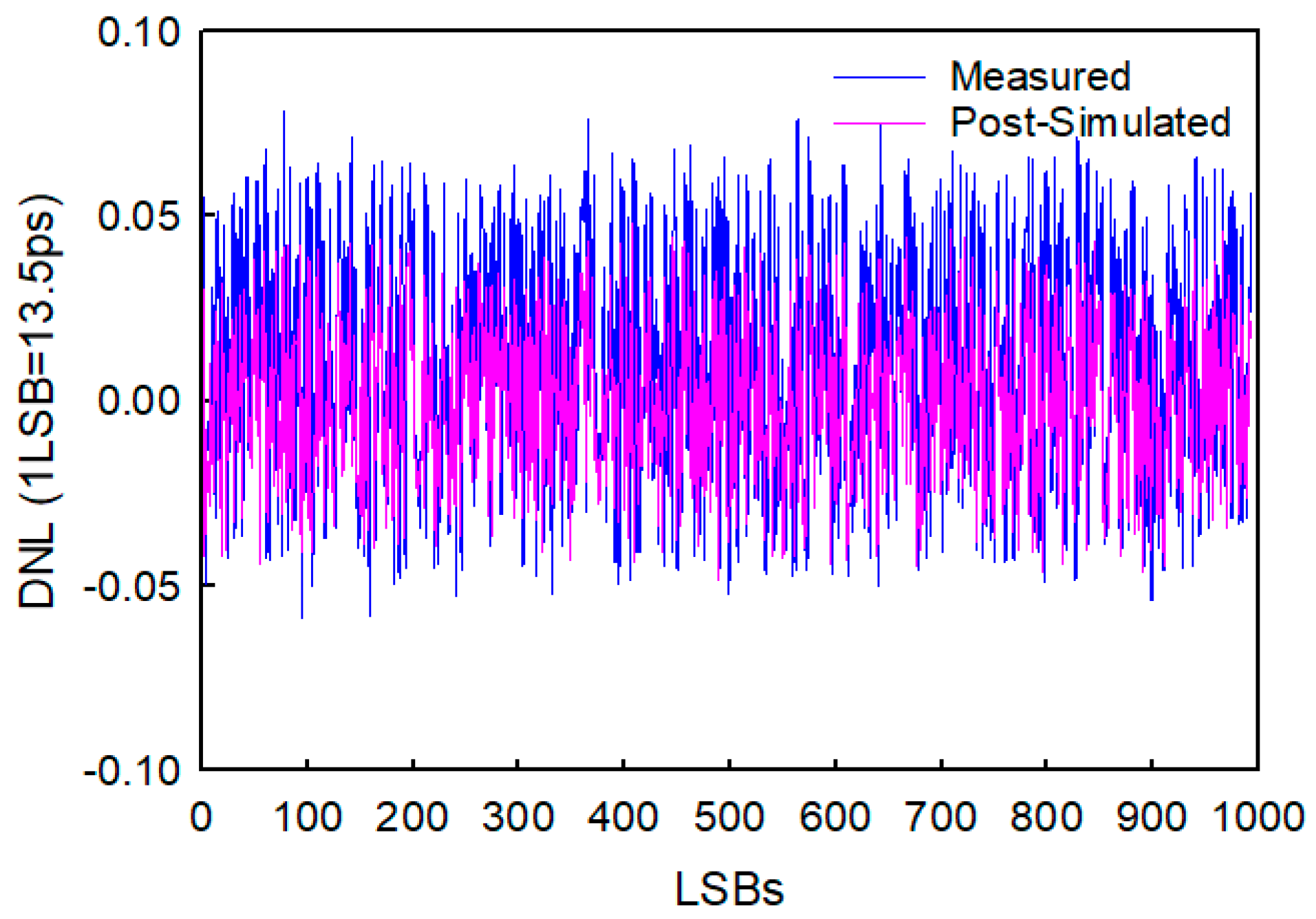
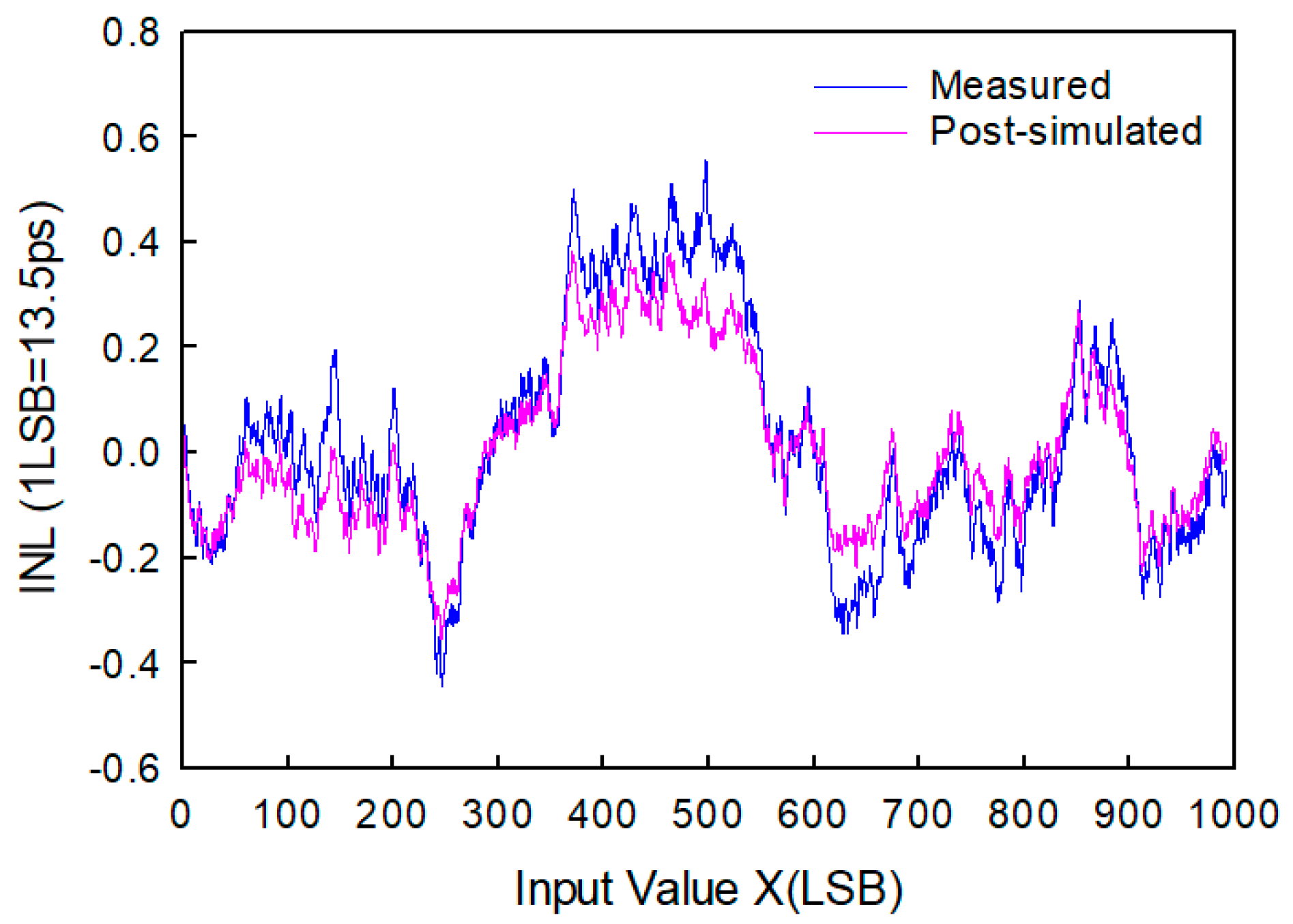
The output interval width of the proposed DTC was accurately measured by a digital oscilloscope (TEK DPO71604C) with 50 GS/s real-time sample rate. The measured and post-synthesis simulated differential nonlinearity (DNL) and integral nonlinearity (INL) of the proposed Cyclone IV E FPGA-DTC are shown in Figure 8 and Figure 9, respectively. The effective resolution is obtained from the measured results. The time difference between START and STOP is nominal to zero when the input value is zero. The measured time interval is 13.392 ns when the input value is 992. The effective resolution is defined as 13.392 ns/992 ≈ 13.5 ps. It can be seen that the measured results are a little worse but approximately the same as the post-synthesis simulated results.
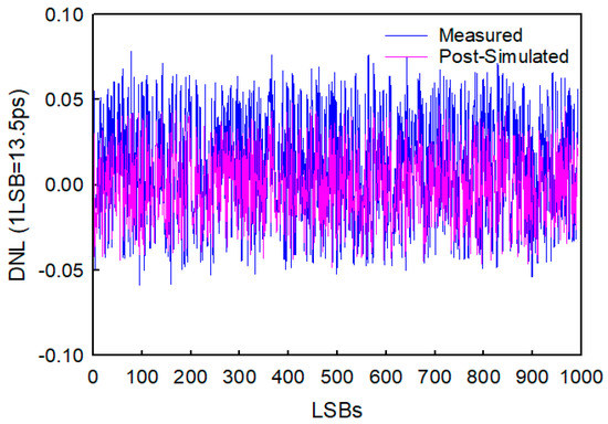
Figure 8.
The post-simulated and measured differential nonlinearity (DNL) of the proposed DTC implemented with Cyclone IV E FPGA.
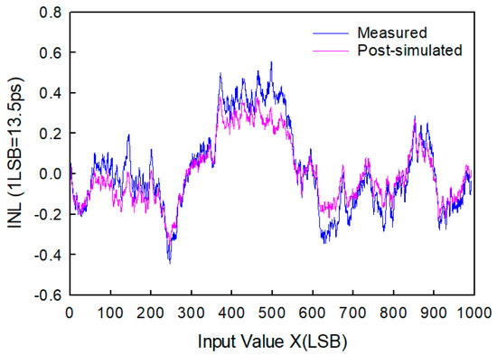
Figure 9.
The post-simulated and measured integral nonlinearity (INL) of the proposed DTC implemented with Cyclone IV E FPGA.
Since the proposed DTC is implemented with PLLs, it is insensitive to device mismatch and shows excellent linearity. The measured DNL and INL are a mere −0.06LSB–0.07LSB and −0.43LSB–0.58LSB, as depicted in Figure 8 and Figure 9, respectively. The proposed DTC utilizes 344 slice look-up-tables (LUTs), 207 registers and 3 PLLs when realized on a Cyclone IV E FPGA with 32 input bits.
3.2. Implementation with Stratix III FPGA
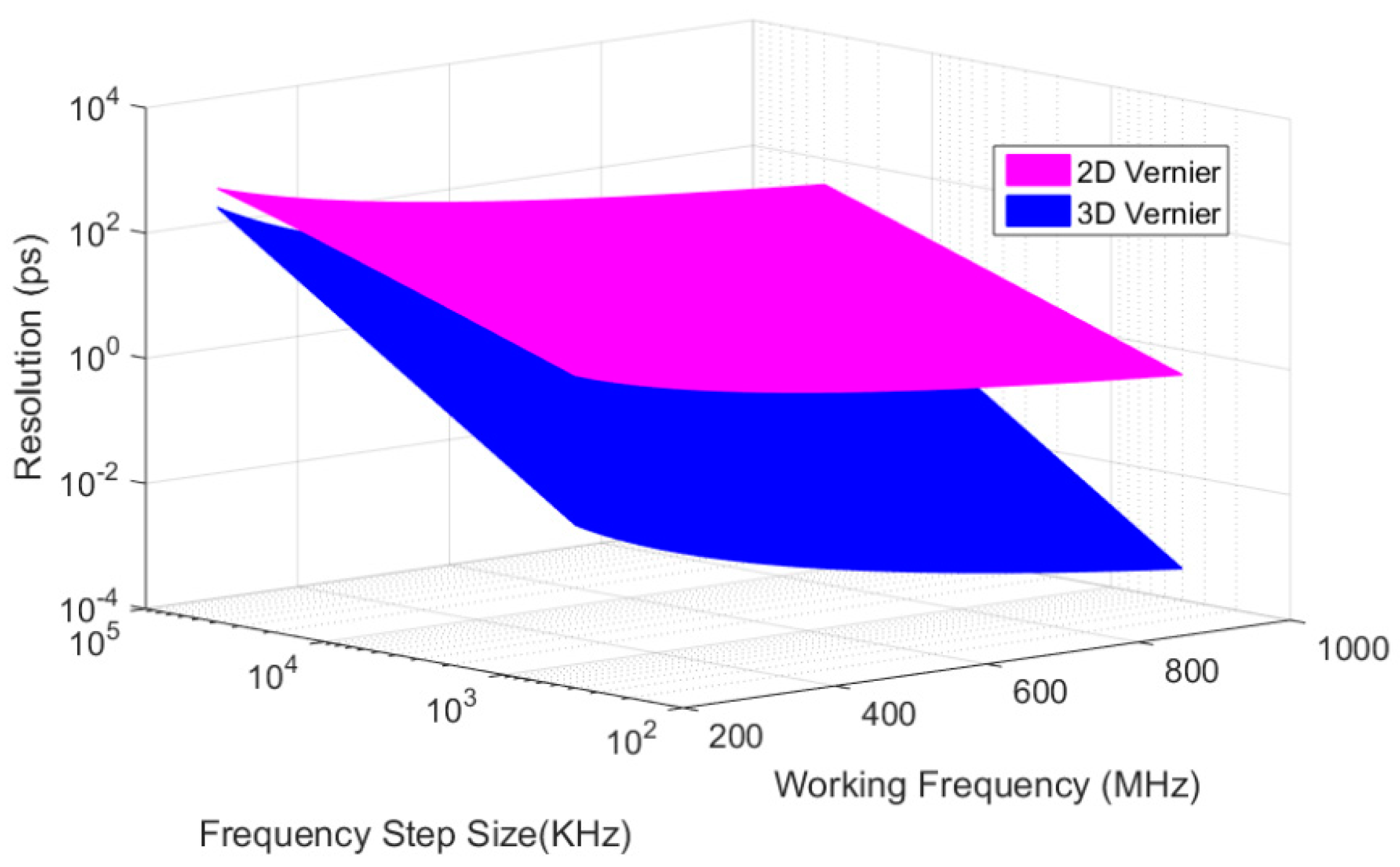
All Cyclone IV E FPGA have a resolution greater than 10 ps, which is similar to the transmission delay lines DTCs. To pursue higher resolution, the higher working frequency and smaller frequency step size are expected. The surface of the expected resolution for a given working frequency and a given frequency step size is shown in Figure 10. It can be seen that the resolution of both the proposed 3D Vernier DTC and 2D scales up when the working frequency increases and the frequency step size decreases. Moreover, the proposed 3D Vernier DTC improved the resolution even more with a high working frequency and small frequency step size. Therefore, the Altera Stratix III EP3SL150F1152C2 FPGA is adopted for performance improvement. The block diagram of PLLs in the Stratix III FPGA is similar to those in Cyclone IV E FPGA. However, in contrast to Cyclone IV E FPGA, the working frequency of Stratix III FPGA can be synthesized much higher. Thus, the resolution can be designed much finer than the Cyclone IV E version. The best resolution is obtained by setting the input frequency to 50 MHz (crystal frequency in DE3-150 system), D to 10, N to 126/127/128, C to 1 (the post scale counter is setting to 2 following VCO included in PLL).

Figure 10.
The time resolution of 2D and 3D Vernier DTC with different working frequency and frequency step size.
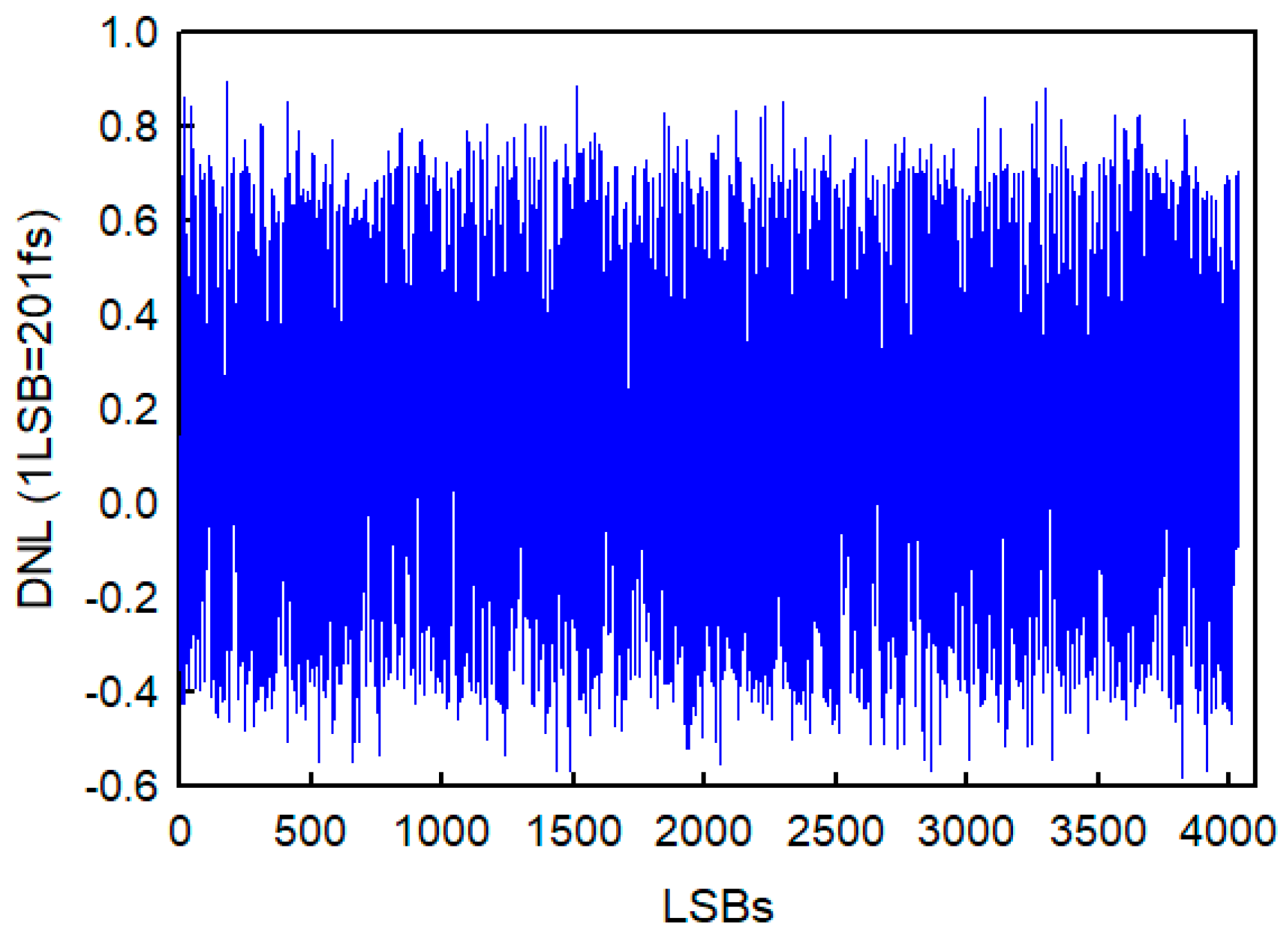
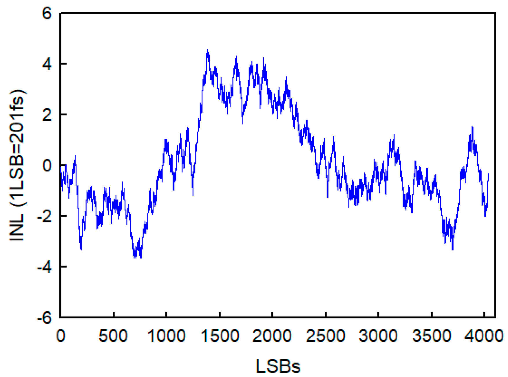
The post-simulated resolution is 203 fs. The post-simulated DNL and INL performance are depicted in Figure 11 and Figure 12, respectively. They are −0.56LSB–0.88LSB and −3.8LSB–4.4LSB as shown in these two figures. The credibility of post-synthesis simulated results has been demonstrated with Cyclone IV E FPGA. The DNL and INL are mainly determined by the mismatch delay time between different transmission paths with different input values. Since the DTCs implemented with two FPGAs have the same topological structure, the INL results display a similar shape. To obtain a lower non-linearity, we should place and route the elements manually with the expenses of interoperability. Moreover, the effective operation range of the proposed DTC can be easily extended by adding input bits. A 54 seconds operation range can be obtained with 48 input bits. The proposed DTC utilizes 448 slice adaptive look-up-tables (ALUTs), 237 registers and 3 PLLs when realized on the Stratix III E FPGA. The specifications for Cyclone IV and Stratix III FPGA DTCs are summarized in Table 2.
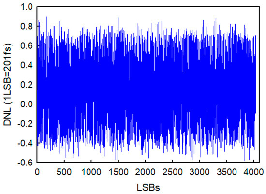
Figure 11.
The post-simulated DNL of the proposed DTC implemented with Stratix III FPGA.
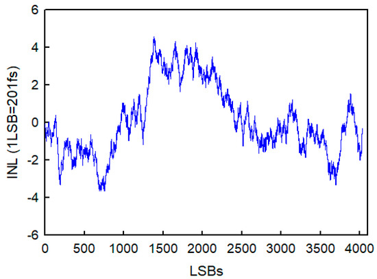
Figure 12.
The post-simulated INL of the proposed DTC implemented with Stratix III FPGA.
Table 2.
Specifications for Cyclone IV and Stratix III FPGA DTCs.
Additionally, the phase noise and jitter of PLLs can transmit to the output signal START and STOP. However, the largest jitter on PLL outputs is smaller than 10 ps and it follows a Gaussian distribution with zero mean value. Thus, the jitter of PLL does not impact the accuracy of the average arithmetic mean measurement.
4. Discussion
The comparison of the proposed DTC and previous DTCs is shown in Table 3. The resolutions of the proposed DTC implemented with 90 nm FPGA and 65 nm FPGA are measured by increasing 992 and 1000 counts, respectively. The measured INL with an input value equal to 2000 is about 3.5 LSBs on Stratix III FPGA. Obviously, the proposed 3D Vernier DTC implemented on Stratix III FPGA DTC has a much higher resolution than all the previous works. With adding an extra dimension, the resolution of the proposed 3D Vernier DTC can be improved by almost two orders of magnitude implemented with the same FPGAs. The dynamic range of proposed DTC can be easily extended by a greater input bit width. Although the nonlinearity of proposed DTC is a little worse than previous FPGA-DTCs with quantization of LSB, the proposed DTC has almost the best absolute nonlinearity quantized by seconds. It is because the proposed 3D Vernier DTC is relying on PLLs to synthesize delays, instead of delay lines or logic gates. Moreover, the proposed DTC can also obtain good resolution implemented with Cyclone IV E FPGAs, which are almost the lowest cost and lowest power consumption FPGAs during all series FPGAs nowadays. Therefore, the proposed FPGA-DTC can be widely used in many applications whether it needs low cost or high resolution.
Table 3.
Performance of the proposed DTC, compared with previous works.
5. Conclusions
In this paper, a novel FPGA-DTC is proposed based on the 3D Vernier principle, which utilizes three PLLs. For principle verification, the proposed method is realized on Cyclone IV E FPGA. It is verified to obtain a measured resolution of 13.5 ps and INL of −0.4–0.43 LSB. To enhance resolution performance, the proposed method also implemented on Stratix III FPGA. The measured results indicate that the resolution of Stratix III FPGA is 203 fs and the post simulated INL is smaller than 1 ps. Moreover, the proposed DTC consumes quite few logic gates and registers with optimized design. Therefore, the proposed FPGA DTC performs excellently for low cost but high accuracy testing applications and instrumentation.
Author Contributions
Conceptualization, C.Y. and J.W.; Data curation, C.Y.; Funding acquisition, C.H. and J.W.; Investigation, C.Y.; Methodology, C.Y.; Resources, C.Y.; Writing–original draft, C.Y.; Writing–review & editing, C.H. and J.W.
Funding
This work is supported by the National Natural Science Foundation of China under project number No.61871118.
Conflicts of Interest
The authors declare no conflict of interest. The funders had no role in the design of the study.
References
- Adabi, E.; Niknejad, A.M. Broadband variable passive delay elements based on an inductance multiplication technique. In Proceedings of the 2008 IEEE Radio Frequency Integrated Circuits Symposium, Atlanta, GA, USA, 15–17 June 2008; pp. 445–448. [Google Scholar]
- Wang, T.Y.; Lin, S.M.; Tsao, H.W. Multiple channel programmable timing generators with single cyclic delay line. IEEE Trans. Instrum. Meas. 2004, 53, 1295–1303. [Google Scholar] [CrossRef]
- Nagaraj, G.; Miller, S.; Stengel, B.; Cafaro, G.; Gradishar, T.; Olson, S.; Hekmann, R. A self-calibrating sub-picosecond resolution digital-totime converter. In Proceedings of the 2007 IEEE/MTT-S International Microwave Symposium, Honolulu, HI, USA, 3–8 June 2007; pp. 2201–2204. [Google Scholar]
- Palattella, C.; Klumperink, E.A.; Ru, J.Z.; Nauta, B. A sensitive method to measure the integral nonlinearity of a digital-to-time converter based on phase modulation. IEEE Trans. Circuits Syst. II Exp. Briefs 2015, 62, 741–745. [Google Scholar] [CrossRef]
- El Mourabit, A.; Lu, G.N.; Pittet, P.; Birjali, Y.; Lahjomri, F. Low power, high resolution CMOS variable-delay element. AEU Int. J. Electron. Commun. 2012, 66, 455–458. [Google Scholar] [CrossRef]
- Vornicu, I.; Carmona-Galán, R.; Rodríguez-Vázquez, Á. Time interval generator with 8 ps resolution and wide range for large TDC array characterization. Analog Integr. Circuits Signal Process. 2016, 87, 181–189. [Google Scholar] [CrossRef]
- Yao, Y.; Wang, Z.; Lu, H.; Chen, L.; Jin, G. Design of time interval generator based on hybrid counting method. Nucl. Instrum. Methods Phys. Res. A, Accel. Spectrom. Detect. Assoc. Equip. 2016, 832, 103–107. [Google Scholar] [CrossRef]
- Zhang, M.; Wang, H.; Liu, Y. Digital-to-Time Converter with 3.93 ps Resolution Implemented on FPGA Chips. IEEE Access 2017, 5, 6842–6848. [Google Scholar] [CrossRef]
- Otsuji, T.I.; Narumi, N. A 3-ns range, 8-ps resolution, timing generator LSI utilizing Si bipolar gate array. IEEE J. Solid-State Circuits 1991, 26, 806–811. [Google Scholar] [CrossRef]
- Arkin, B. Realizing a production ATE custom processor and timing IC containing 400 independent low-power and high-linearity timing verniers. In Proceedings of the 2004 IEEE International Solid-State Circuits Conference (IEEE Cat. No.04CH37519), San Francisco, CA, USA, 15–19 February 2004; pp. 348–349. [Google Scholar]
- Chen, P.; Chen, P.Y.; Lai, J.S.; Chen, Y.J. FPGA vernier digital-to-time converter with 1.58 ps resolution and 59.3 minutes operation range. IEEE Trans. Circuits Syst. I: Reg. Papers 2010, 57, 1134–1142. [Google Scholar] [CrossRef]
- Klepacki, K.; Pawłowski, M.; Szplet, R. Low-jitter wide-range integrated time interval/delay generator based on combination of period counting and capacitor charging. Rev. Sci. Instrum. 2015, 86, 025111. [Google Scholar] [CrossRef] [PubMed]
- Rahkonen, T.E.; Kostamovaara, J.T. The use of stabilized CMOS delay line for the digitization of short time intervals. IEEE J. Solid State Circuits 1993, 28, 887–894. [Google Scholar] [CrossRef]
- Quartus II Version 8.0 Handbook, Volume 2. Design Implementation and Optimization: Section II. Area, Timing, and Power Optimization. Altera Corp. Available online: www.altera.com (accessed on 30 June 2008).
- Quartus II Version 8.0 Handbook, Volume 3. Verification: Section II. Timing Analysis, Altera Corp. Available online: www.altera.com (accessed on 30 June 2008).
- Clock Networks and PLLs in Cyclone IV Devices Altera Corp. Available online: www.altera.com (accessed on 30 October 2012).
- Clock Networks and PLLs in Stratix III Devices. Altera Corp. Available online: www.altera.com (accessed on 31 July 2009).
- Lai, C.M.; Wu, J.M.; Huang, P.C.; Chu, T.S. A scalable direct sampling broadband radar receiver supporting simultaneous digital multi beam array in 65 nm CMOS. In Proceedings of the 2013 IEEE International Solid-State Circuits Conference Digest of Technical Papers, San Francisco, CA, USA, 17–21 February 2013; pp. 242–243. [Google Scholar]
- Wang, H.; Zhang, M.; Liu, Y. High-resolution digital-to-time converter implemented in an FPGA chip. Appl. Sci. 2017, 7, 52. [Google Scholar] [CrossRef]

© 2019 by the authors. Licensee MDPI, Basel, Switzerland. This article is an open access article distributed under the terms and conditions of the Creative Commons Attribution (CC BY) license (http://creativecommons.org/licenses/by/4.0/).