RNA–CTMA Dielectrics in Organic Field Effect Transistor Memory


Abstract
:1. Introduction
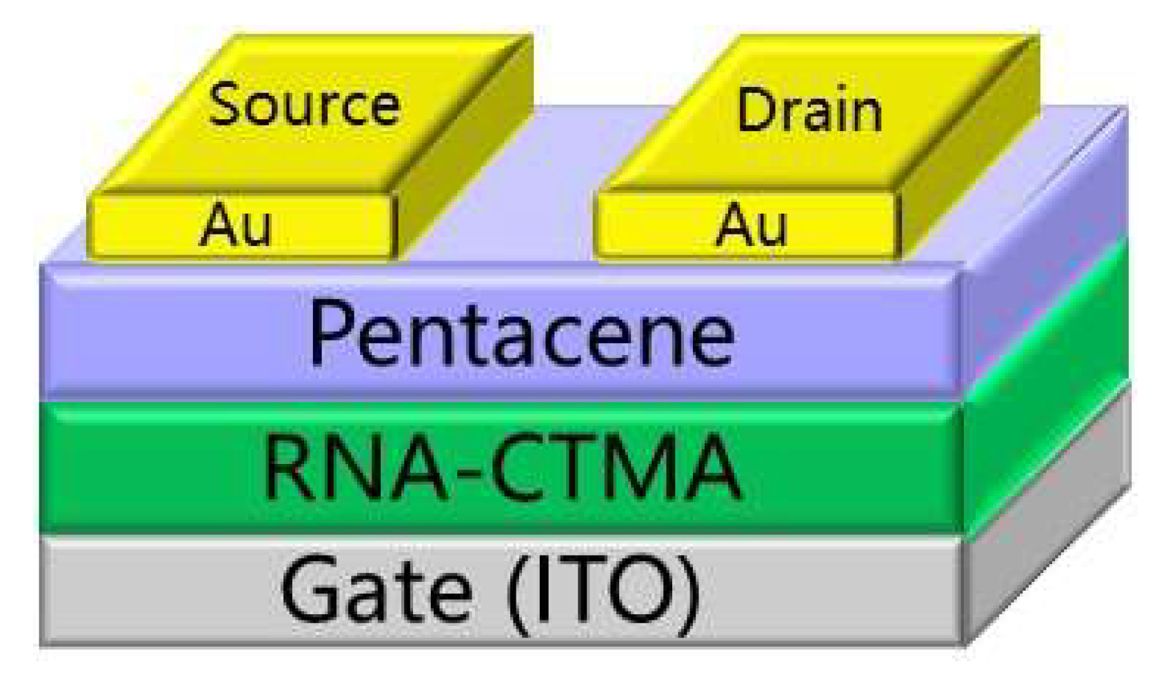
2. Experimental
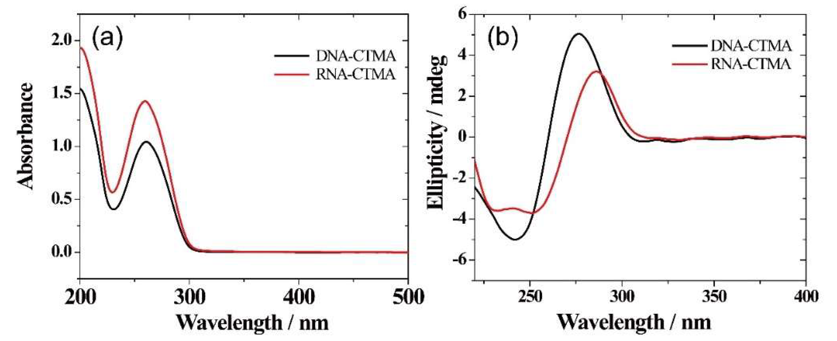
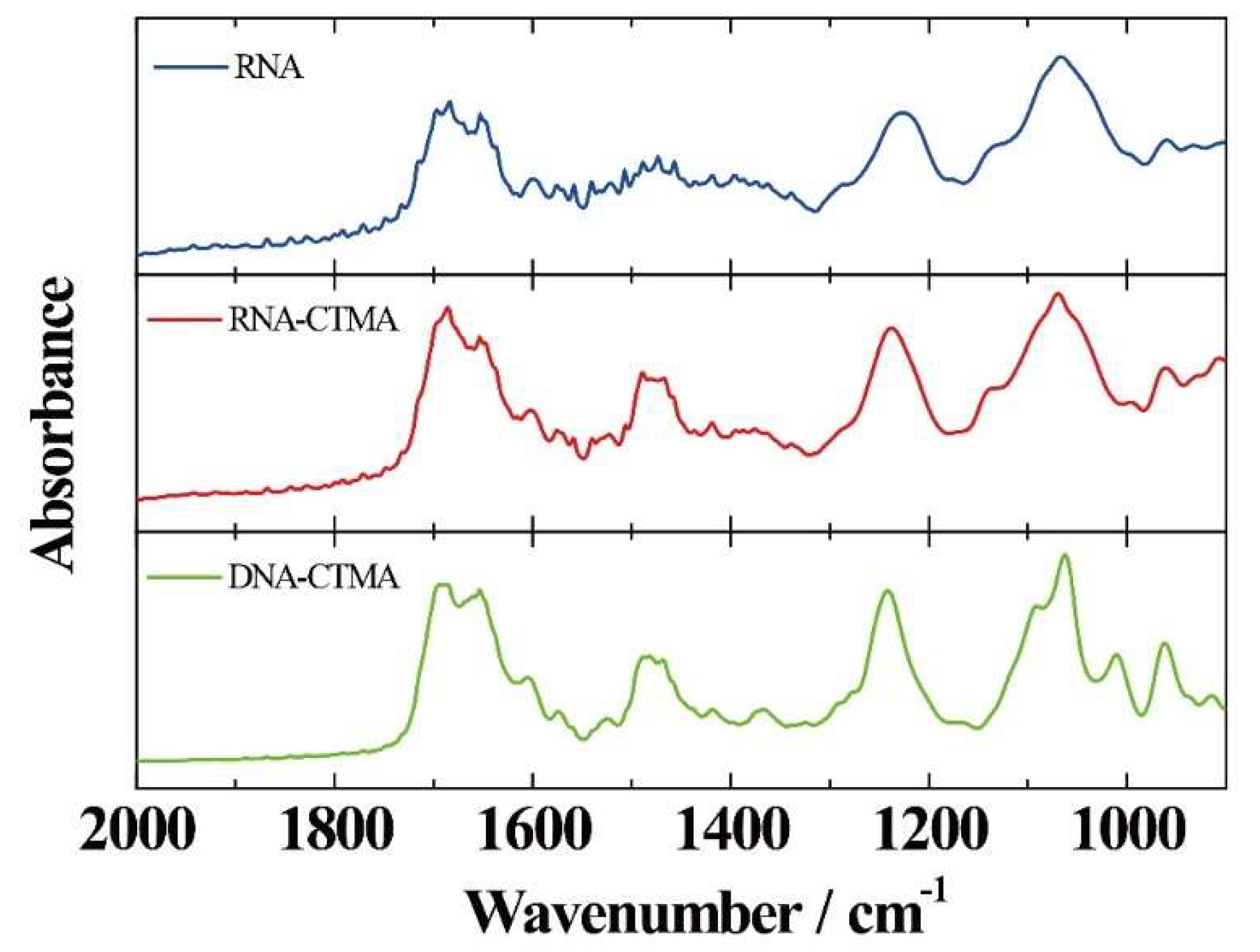
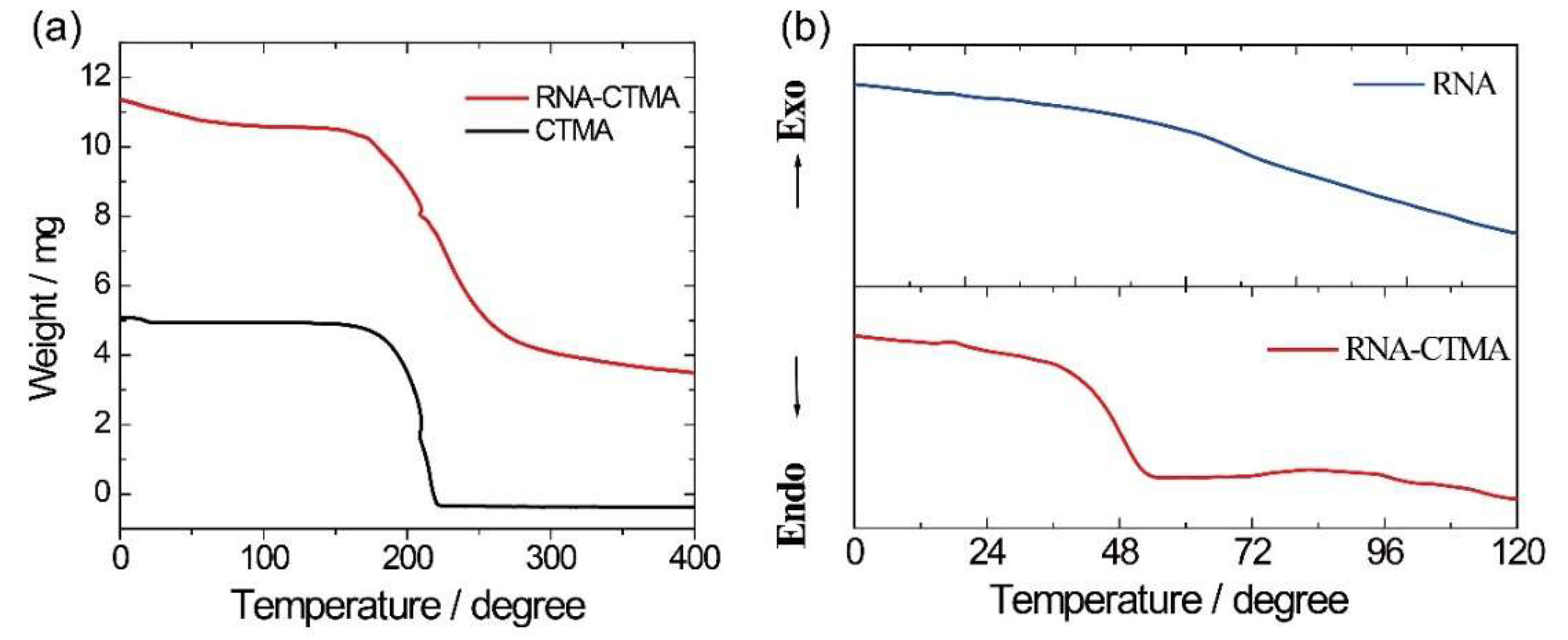
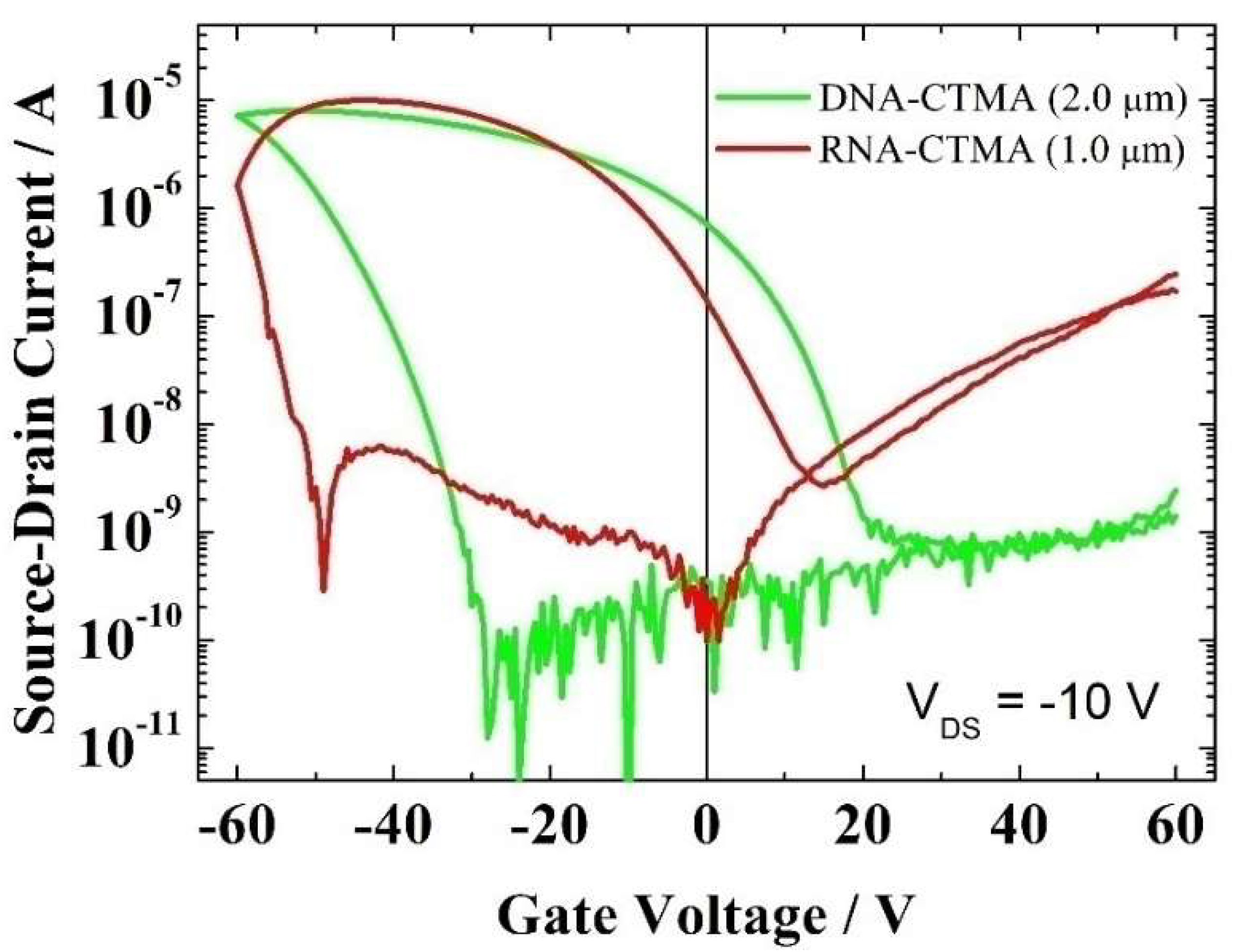
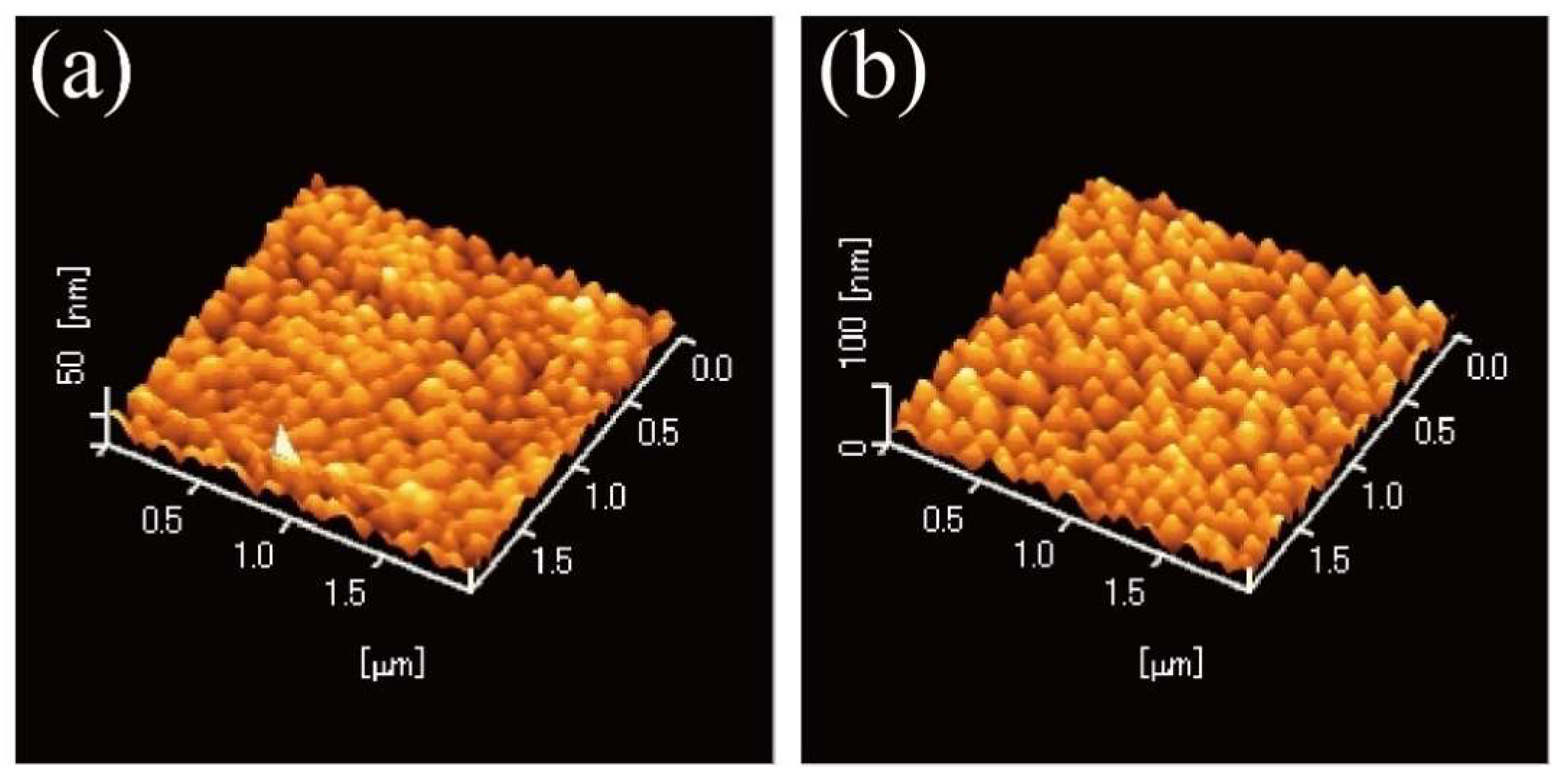
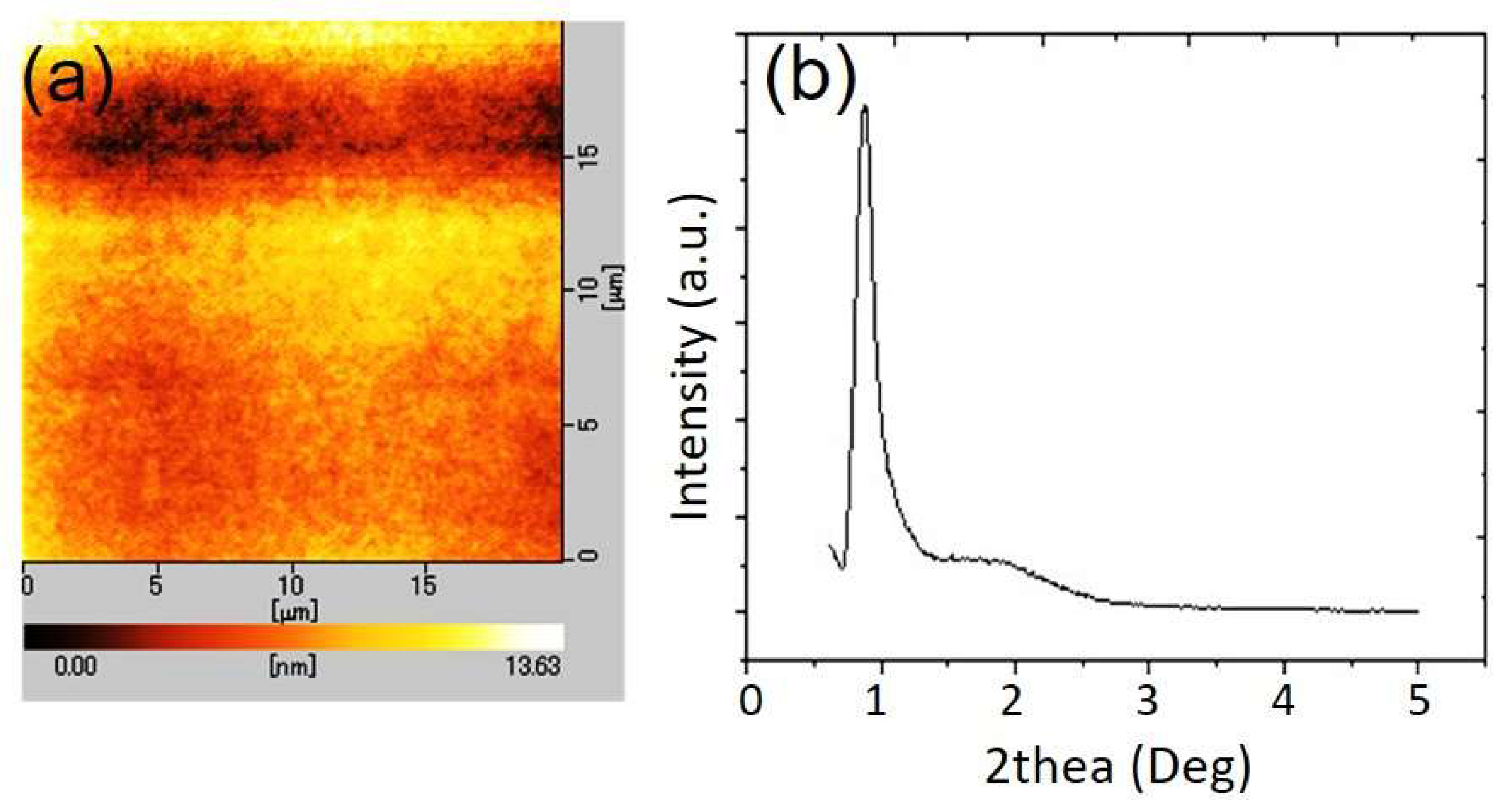
3. Results and Discussion
4. Conclusions
Author Contributions
Funding
Conflicts of Interest
References
- Magliulo, M.; Manoli, K.; Macchia, E.; Palazzo, G.; Torsi, L. Tailoring Functional Interlayers in Organic Field-Effect Transistor Biosensors. Adv. Mater. 2015, 27, 7528–7551. [Google Scholar] [CrossRef] [PubMed]
- Chang, J.W.; Wang, C.G.; Huang, C.Y.; Tsai, T.D.; Guo, T.F.; Wen, T.C. Chicken Albumen Dielectrics in Organic Field-Effect Transistors. Adv. Mater. 2011, 23, 4077–4081. [Google Scholar] [CrossRef] [PubMed]
- Kim, S.J.; Jeon, D.B.; Park, J.H.; Ryu, M.K.; Yang, J.H.; Hwang, C.S.; Kim, G.H.; Yoon, S.M. Nonvolatile memory thin-film transistors using biodegradable chicken albumen gate insulator and oxide semiconductor channel on eco-friendly paper substrate. ACS Appl. Mater. Interfaces 2015, 7, 4869–4874. [Google Scholar] [CrossRef] [PubMed]
- Kim, Y.S.; Jung, K.H.; Lee, U.R.; Kim, K.H.; Hoang, M.H.; Jin, J.-I.; Choi, D.H. High-performance, low-operating voltage, and solution-processable organic field-effect transistor with silk fibroin as the gate dielectric. App. Phys. Lett. 2014, 96. [Google Scholar] [CrossRef]
- Stadler, P.; Oppelt, K.; Singh, T.B.; Grote, J.G.; Schwödiauer, R.; Bauer, S.; Brezina, H.P.; Bäuerle, D.; Sariciftci, N.S. Organic field-effect transistors and memory elements using deoxyribonucleic acid (DNA) gate dielectric. Org. Electron. 2007, 8, 648. [Google Scholar] [CrossRef]
- Jeng, H.Y.; Yang, T.C.; Yang, L.; Grote, J.G.; Chen, H.L.; Hung, Y.C. Non-volatile resistive memory device based on solution-processed natural DNA biomaterial. Org. Electron. 2017, 54, 216–221. [Google Scholar] [CrossRef]
- Zhou, L.; Wanga, A.; Wu, S.C.; Sun, J.; Park, S.; Jackson, T.N. All-organic active matrix flexible display. Appl. Phys. Lett. 2006, 88, 083502. [Google Scholar] [CrossRef]
- Baude, P.F.; Ender, D.A.; Haase, M.A.; Kelley, T.W.; Muyres, D.V.; Theiss, S.D. Pentacene-based radio-frequency identification circuitry. Appl. Phys. Lett. 2003, 82, 3964–3966. [Google Scholar] [CrossRef]
- Parashkov, R.; Becker, E.; Ginev, G.; Riedl, T.; Brandes, M.; Johannes, H.H.; Kowalsky, W. Organic vertical-channel transistors structured using excimer laser. Appl. Phys. Lett. 2004, 85, 5751–5753. [Google Scholar] [CrossRef]
- Naber, R.C.G.; Asadi, K.; Blom, P.W.M.; Leeuw, D.M.D.; Boer, B.D. Organic Nonvolatile Memory Devices Based on Ferroelectricity. Adv. Mater. 2010, 22, 933–945. [Google Scholar] [CrossRef] [PubMed]
- Tanaka, K.; Okahata, Y. A DNA−Lipid Complex in Organic Media and Formation of an Aligned Cast Film1. J. Am. Chem. Soc. 1996, 118, 10679. [Google Scholar] [CrossRef]
- Zalar, P.; Kamkar, D.; Naik, R.; Ouchen, F.; Grote, J.G.; Bazan, G.C.; Nguyen, T.-Q. DNA electron injection interlayers for polymer light-emitting diodes. J. Am. Chem. Soc. 2011, 133, 11010. [Google Scholar] [CrossRef] [PubMed]
- Grykien, R.; Luszczynska, B.; Glowacki, I.; Ulanski, J.; Kajzar, F.; Zgarian, R.; Rau, I. A significant improvement of luminance vs current density efficiency of a BioLED. Opt. Mater. 2014, 36, 1027. [Google Scholar] [CrossRef]
- Gomez, E.F.; Venkatraman, V.; Grote, J.G.; Steckl, A.J. Exploring the Potential of Nucleic Acid Bases in Organic Light Emitting Diodes. Adv. Mater. 2015, 27, 7552. [Google Scholar] [CrossRef] [PubMed]
- Gomez, E.F.; Venkatraman, V.; Grote, J.G.; Steckl, A. DNA Bases Thymine and Adenine in Bio-Organic Light Emitting Diodes. Sci. Rep. 2014, 4, 7105. [Google Scholar] [CrossRef] [PubMed]
- Yusoff, A.; bin Mohd, R.; Kim, J.; Jang, J.; Nazeeruddin, M.K. New Horizons for Perovskite Solar Cells Employing DNA-CTMA as the Hole-Transporting Material. ChemSusChem 2016, 9, 1736–1742. [Google Scholar] [CrossRef] [PubMed]
- Kumar, A.; Shukla, R.D.; Yadav, D.; Gupta, L.P. Friedel–Crafts alkylation of indoles in deep eutectic solvent. RSC Adv. 2015, 5, 52062–52065. [Google Scholar] [CrossRef]
- Ensslen, P.; Gärtner, S.; Glaser, K.; Colsmann, A.; Wagenknecht, H.-A. A DNA–Fullerene Conjugate as a Template for Supramolecular Chromophore Assemblies: Towards DNA-Based Solar Cells. Angew. Chem. Int. Ed. 2016, 55, 1904–1908. [Google Scholar] [CrossRef] [PubMed]
- Liang, L.; Yukimoto, T.; Uemura, S.; Kamata, T.; Nakamura, K.; Kobayashi, N. Structure of DNA-Octadecyltrimethylammonium Chloride Biopolymer Complex and the Application to Non-Volatile BiOTFT Memory. Sci. Adv. Mater. 2014, 6, 1516–1519. [Google Scholar] [CrossRef]
- Liang, L.; Mitsumura, Y.; Nakamura, K.; Uemura, S.; Kamata, T.; Kobayashi, N. Temperature dependence of transfer characteristics of OTFT memory based on DNA-CTMA gate dielectric. Org. Electron. 2016, 28, 294–298. [Google Scholar] [CrossRef]
- Yukimoto, T.; Uemura, S.; Kamata, T.; Nakamura, K.; Kobayashi, N. Non-volatile transistor memory fabricated using DNA and eliminating influence of mobile ions on electric properties. J. Mater. Chem. C 2011, 21, 15575. [Google Scholar] [CrossRef]
- Grote, J.G.; Hopkins, F.K. Bio-organic semiconductor-field-effect-transistor based on deoxyribonucleic acid gate dielectric. Appl. Phys. 2006, 100, 024514. [Google Scholar]
- Kwon, Y.W.; Lee, C.H.; Choi, D.H.; Jin, J.I. Materials science of DNA. J. Mater. Chem. 2009, 19, 1353–1380. [Google Scholar] [CrossRef]
- Steckl, A.J.; Spaeth, H.; You, H.; Gomez, E.; Grote, J. DNA as an optical material. Opt. Photonics News 2011, 22, 34–39. [Google Scholar] [CrossRef]
- Deman, A.L.; Erouel, M.; Lallemand, D.; Goutorbe, M.P.; Lang, P.; Tardy, J. Growth related properties of pentacene thin film transistors with different gate dielectrics. J. Non-Cryst. Solids 2008, 354, 1598–1607. [Google Scholar] [CrossRef]


| RNA | RNA–CTMA | DNA–CTMA | Assignments |
|---|---|---|---|
| 1226 | 1237 | 1240 | PO2 antisymmetric |
| 1127 | 1134 | 1089 | PO2 symmetric |
| 1066 | 1069 | 1062 | C–O sugar |
| 1000 | 996 | 1010 | Sugar ring |
© 2018 by the authors. Licensee MDPI, Basel, Switzerland. This article is an open access article distributed under the terms and conditions of the Creative Commons Attribution (CC BY) license (http://creativecommons.org/licenses/by/4.0/).
Share and Cite
Liang, L.; Fu, Y.; Li, L.; Zheng, H.; Wei, X.; Wei, Y.; Kobayashi, N. RNA–CTMA Dielectrics in Organic Field Effect Transistor Memory. Appl. Sci. 2018, 8, 887. https://doi.org/10.3390/app8060887
Liang L, Fu Y, Li L, Zheng H, Wei X, Wei Y, Kobayashi N. RNA–CTMA Dielectrics in Organic Field Effect Transistor Memory. Applied Sciences. 2018; 8(6):887. https://doi.org/10.3390/app8060887
Chicago/Turabian StyleLiang, Lijuan, Yabo Fu, Lianfang Li, Huan Zheng, Xianfu Wei, Yen Wei, and Norihisa Kobayashi. 2018. "RNA–CTMA Dielectrics in Organic Field Effect Transistor Memory" Applied Sciences 8, no. 6: 887. https://doi.org/10.3390/app8060887
APA StyleLiang, L., Fu, Y., Li, L., Zheng, H., Wei, X., Wei, Y., & Kobayashi, N. (2018). RNA–CTMA Dielectrics in Organic Field Effect Transistor Memory. Applied Sciences, 8(6), 887. https://doi.org/10.3390/app8060887